EP1672093B1 - Film-forming apparatus and film-forming method - Google Patents
Film-forming apparatus and film-forming method Download PDFInfo
- Publication number
- EP1672093B1 EP1672093B1 EP04773039.5A EP04773039A EP1672093B1 EP 1672093 B1 EP1672093 B1 EP 1672093B1 EP 04773039 A EP04773039 A EP 04773039A EP 1672093 B1 EP1672093 B1 EP 1672093B1
- Authority
- EP
- European Patent Office
- Prior art keywords
- deposition
- gas
- chamber
- substrate
- plasma generation
- Prior art date
- Legal status (The legal status is an assumption and is not a legal conclusion. Google has not performed a legal analysis and makes no representation as to the accuracy of the status listed.)
- Expired - Lifetime
Links
Images


Classifications
-
- H—ELECTRICITY
- H01—ELECTRIC ELEMENTS
- H01J—ELECTRIC DISCHARGE TUBES OR DISCHARGE LAMPS
- H01J37/00—Discharge tubes with provision for introducing objects or material to be exposed to the discharge, e.g. for the purpose of examination or processing thereof
- H01J37/32—Gas-filled discharge tubes
- H01J37/32009—Arrangements for generation of plasma specially adapted for examination or treatment of objects, e.g. plasma sources
- H01J37/32192—Microwave generated discharge
-
- C—CHEMISTRY; METALLURGY
- C23—COATING METALLIC MATERIAL; COATING MATERIAL WITH METALLIC MATERIAL; CHEMICAL SURFACE TREATMENT; DIFFUSION TREATMENT OF METALLIC MATERIAL; COATING BY VACUUM EVAPORATION, BY SPUTTERING, BY ION IMPLANTATION OR BY CHEMICAL VAPOUR DEPOSITION, IN GENERAL; INHIBITING CORROSION OF METALLIC MATERIAL OR INCRUSTATION IN GENERAL
- C23C—COATING METALLIC MATERIAL; COATING MATERIAL WITH METALLIC MATERIAL; SURFACE TREATMENT OF METALLIC MATERIAL BY DIFFUSION INTO THE SURFACE, BY CHEMICAL CONVERSION OR SUBSTITUTION; COATING BY VACUUM EVAPORATION, BY SPUTTERING, BY ION IMPLANTATION OR BY CHEMICAL VAPOUR DEPOSITION, IN GENERAL
- C23C16/00—Chemical coating by decomposition of gaseous compounds, without leaving reaction products of surface material in the coating, i.e. chemical vapour deposition [CVD] processes
- C23C16/44—Chemical coating by decomposition of gaseous compounds, without leaving reaction products of surface material in the coating, i.e. chemical vapour deposition [CVD] processes characterised by the method of coating
- C23C16/455—Chemical coating by decomposition of gaseous compounds, without leaving reaction products of surface material in the coating, i.e. chemical vapour deposition [CVD] processes characterised by the method of coating characterised by the method used for introducing gases into reaction chamber or for modifying gas flows in reaction chamber
-
- C—CHEMISTRY; METALLURGY
- C23—COATING METALLIC MATERIAL; COATING MATERIAL WITH METALLIC MATERIAL; CHEMICAL SURFACE TREATMENT; DIFFUSION TREATMENT OF METALLIC MATERIAL; COATING BY VACUUM EVAPORATION, BY SPUTTERING, BY ION IMPLANTATION OR BY CHEMICAL VAPOUR DEPOSITION, IN GENERAL; INHIBITING CORROSION OF METALLIC MATERIAL OR INCRUSTATION IN GENERAL
- C23C—COATING METALLIC MATERIAL; COATING MATERIAL WITH METALLIC MATERIAL; SURFACE TREATMENT OF METALLIC MATERIAL BY DIFFUSION INTO THE SURFACE, BY CHEMICAL CONVERSION OR SUBSTITUTION; COATING BY VACUUM EVAPORATION, BY SPUTTERING, BY ION IMPLANTATION OR BY CHEMICAL VAPOUR DEPOSITION, IN GENERAL
- C23C16/00—Chemical coating by decomposition of gaseous compounds, without leaving reaction products of surface material in the coating, i.e. chemical vapour deposition [CVD] processes
- C23C16/44—Chemical coating by decomposition of gaseous compounds, without leaving reaction products of surface material in the coating, i.e. chemical vapour deposition [CVD] processes characterised by the method of coating
- C23C16/448—Chemical coating by decomposition of gaseous compounds, without leaving reaction products of surface material in the coating, i.e. chemical vapour deposition [CVD] processes characterised by the method of coating characterised by the method used for generating reactive gas streams, e.g. by evaporation or sublimation of precursor materials
- C23C16/452—Chemical coating by decomposition of gaseous compounds, without leaving reaction products of surface material in the coating, i.e. chemical vapour deposition [CVD] processes characterised by the method of coating characterised by the method used for generating reactive gas streams, e.g. by evaporation or sublimation of precursor materials by activating reactive gas streams before their introduction into the reaction chamber, e.g. by ionisation or addition of reactive species
-
- C—CHEMISTRY; METALLURGY
- C23—COATING METALLIC MATERIAL; COATING MATERIAL WITH METALLIC MATERIAL; CHEMICAL SURFACE TREATMENT; DIFFUSION TREATMENT OF METALLIC MATERIAL; COATING BY VACUUM EVAPORATION, BY SPUTTERING, BY ION IMPLANTATION OR BY CHEMICAL VAPOUR DEPOSITION, IN GENERAL; INHIBITING CORROSION OF METALLIC MATERIAL OR INCRUSTATION IN GENERAL
- C23C—COATING METALLIC MATERIAL; COATING MATERIAL WITH METALLIC MATERIAL; SURFACE TREATMENT OF METALLIC MATERIAL BY DIFFUSION INTO THE SURFACE, BY CHEMICAL CONVERSION OR SUBSTITUTION; COATING BY VACUUM EVAPORATION, BY SPUTTERING, BY ION IMPLANTATION OR BY CHEMICAL VAPOUR DEPOSITION, IN GENERAL
- C23C16/00—Chemical coating by decomposition of gaseous compounds, without leaving reaction products of surface material in the coating, i.e. chemical vapour deposition [CVD] processes
- C23C16/44—Chemical coating by decomposition of gaseous compounds, without leaving reaction products of surface material in the coating, i.e. chemical vapour deposition [CVD] processes characterised by the method of coating
- C23C16/50—Chemical coating by decomposition of gaseous compounds, without leaving reaction products of surface material in the coating, i.e. chemical vapour deposition [CVD] processes characterised by the method of coating using electric discharges
- C23C16/505—Chemical coating by decomposition of gaseous compounds, without leaving reaction products of surface material in the coating, i.e. chemical vapour deposition [CVD] processes characterised by the method of coating using electric discharges using radio frequency discharges
- C23C16/509—Chemical coating by decomposition of gaseous compounds, without leaving reaction products of surface material in the coating, i.e. chemical vapour deposition [CVD] processes characterised by the method of coating using electric discharges using radio frequency discharges using internal electrodes
- C23C16/5096—Flat-bed apparatus
-
- C—CHEMISTRY; METALLURGY
- C23—COATING METALLIC MATERIAL; COATING MATERIAL WITH METALLIC MATERIAL; CHEMICAL SURFACE TREATMENT; DIFFUSION TREATMENT OF METALLIC MATERIAL; COATING BY VACUUM EVAPORATION, BY SPUTTERING, BY ION IMPLANTATION OR BY CHEMICAL VAPOUR DEPOSITION, IN GENERAL; INHIBITING CORROSION OF METALLIC MATERIAL OR INCRUSTATION IN GENERAL
- C23C—COATING METALLIC MATERIAL; COATING MATERIAL WITH METALLIC MATERIAL; SURFACE TREATMENT OF METALLIC MATERIAL BY DIFFUSION INTO THE SURFACE, BY CHEMICAL CONVERSION OR SUBSTITUTION; COATING BY VACUUM EVAPORATION, BY SPUTTERING, BY ION IMPLANTATION OR BY CHEMICAL VAPOUR DEPOSITION, IN GENERAL
- C23C16/00—Chemical coating by decomposition of gaseous compounds, without leaving reaction products of surface material in the coating, i.e. chemical vapour deposition [CVD] processes
- C23C16/44—Chemical coating by decomposition of gaseous compounds, without leaving reaction products of surface material in the coating, i.e. chemical vapour deposition [CVD] processes characterised by the method of coating
- C23C16/50—Chemical coating by decomposition of gaseous compounds, without leaving reaction products of surface material in the coating, i.e. chemical vapour deposition [CVD] processes characterised by the method of coating using electric discharges
- C23C16/511—Chemical coating by decomposition of gaseous compounds, without leaving reaction products of surface material in the coating, i.e. chemical vapour deposition [CVD] processes characterised by the method of coating using electric discharges using microwave discharges
-
- H—ELECTRICITY
- H01—ELECTRIC ELEMENTS
- H01J—ELECTRIC DISCHARGE TUBES OR DISCHARGE LAMPS
- H01J37/00—Discharge tubes with provision for introducing objects or material to be exposed to the discharge, e.g. for the purpose of examination or processing thereof
- H01J37/32—Gas-filled discharge tubes
- H01J37/32009—Arrangements for generation of plasma specially adapted for examination or treatment of objects, e.g. plasma sources
- H01J37/32357—Generation remote from the workpiece, e.g. down-stream
-
- H—ELECTRICITY
- H01—ELECTRIC ELEMENTS
- H01L—SEMICONDUCTOR DEVICES NOT COVERED BY CLASS H10
- H01L21/00—Processes or apparatus adapted for the manufacture or treatment of semiconductor or solid state devices or of parts thereof
- H01L21/02—Manufacture or treatment of semiconductor devices or of parts thereof
- H01L21/04—Manufacture or treatment of semiconductor devices or of parts thereof the devices having potential barriers, e.g. a PN junction, depletion layer or carrier concentration layer
- H01L21/18—Manufacture or treatment of semiconductor devices or of parts thereof the devices having potential barriers, e.g. a PN junction, depletion layer or carrier concentration layer the devices having semiconductor bodies comprising elements of Group IV of the Periodic Table or AIIIBV compounds with or without impurities, e.g. doping materials
- H01L21/30—Treatment of semiconductor bodies using processes or apparatus not provided for in groups H01L21/20 - H01L21/26
- H01L21/31—Treatment of semiconductor bodies using processes or apparatus not provided for in groups H01L21/20 - H01L21/26 to form insulating layers thereon, e.g. for masking or by using photolithographic techniques; After treatment of these layers; Selection of materials for these layers
-
- H—ELECTRICITY
- H01—ELECTRIC ELEMENTS
- H01L—SEMICONDUCTOR DEVICES NOT COVERED BY CLASS H10
- H01L21/00—Processes or apparatus adapted for the manufacture or treatment of semiconductor or solid state devices or of parts thereof
- H01L21/02—Manufacture or treatment of semiconductor devices or of parts thereof
- H01L21/02104—Forming layers
- H01L21/02107—Forming insulating materials on a substrate
- H01L21/02225—Forming insulating materials on a substrate characterised by the process for the formation of the insulating layer
- H01L21/0226—Forming insulating materials on a substrate characterised by the process for the formation of the insulating layer formation by a deposition process
- H01L21/02263—Forming insulating materials on a substrate characterised by the process for the formation of the insulating layer formation by a deposition process deposition from the gas or vapour phase
- H01L21/02271—Forming insulating materials on a substrate characterised by the process for the formation of the insulating layer formation by a deposition process deposition from the gas or vapour phase deposition by decomposition or reaction of gaseous or vapour phase compounds, i.e. chemical vapour deposition
- H01L21/02274—Forming insulating materials on a substrate characterised by the process for the formation of the insulating layer formation by a deposition process deposition from the gas or vapour phase deposition by decomposition or reaction of gaseous or vapour phase compounds, i.e. chemical vapour deposition in the presence of a plasma [PECVD]
Definitions
- a deposition apparatus and a deposition method using CVD are disclosed in Japanese Unexamined Patent Publication No. 2001-185546 and in Japanese National Publication of International Application No. 2002-539326 .
- US 2001/0042512 A1 discloses a CVD apparatus which produces plasma to generate radicals and uses the radicals, together with silane and the like, to deposit films on substrates in a vacuum vessel.
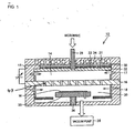
- the vacuum vessel has a partitioning wall section for separating the inside thereof into a plasma-generating space and a film deposition process space.
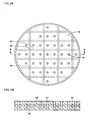
- the partitioning wall section has a plurality of through-holes and diffusion holes.
- An interior space receives the silane or the like fed into the film deposition process space through diffusion holes.
- the radicals produced in the plasma-generating space are fed into the film deposition process space through the through-holes.
- a diameter of the hole is so constituted that a pressure difference between the plasma generation chamber and the deposition chamber becomes 1.5 times or more.
- the distribution plate is preferably formed of carbon, silicon or aluminum.
- the step of continuously polymerizing the deposition component through the radical comprises a step of continuously generating the radical and a step of supplying the deposition gas to the deposition region according to the desired film, the step of continuously generating the radical is performed at a first pressure, the step of supplying the deposition gas to the deposition region according to the desired film is performed at a second pressure, and the first pressure is at least 1.5 times as high as the second pressure.
- the holes are formed in the distribution plate 16 provided between the plasma generation chamber 14 and the deposition chamber 20 so that a pressure in the plasma generation chamber 14 becomes positive as compared with the pressure in the deposition chamber 20 by a predetermined pressure difference. That is, a diameter of the hole is selected so that at least 1.5-fold pressure difference may be generated, and preferably 2-fold pressure difference or more may be generated between both chambers. More specifically, although it is preferable that a hole diameter is 1mm and a hole depth is 5mm or more, it depends on a treatment gas flow rate.
- the isolating plate 16 although carbon is preferable, aluminum or silicon may be used.
- a radical and /or an inert gas having a desired polarity of radicals generated in the plasma generation chamber 14 and a charged inert gas can be selectively taken out through the hole or neutralized.
- positively charged argon Ar + or hydrogen H + radical can be drawn into the deposition chamber 20 or neutralized to cause a desired reaction.
Landscapes
- Chemical & Material Sciences (AREA)
- Engineering & Computer Science (AREA)
- Physics & Mathematics (AREA)
- Plasma & Fusion (AREA)
- Mechanical Engineering (AREA)
- Organic Chemistry (AREA)
- Metallurgy (AREA)
- Materials Engineering (AREA)
- Chemical Kinetics & Catalysis (AREA)
- General Chemical & Material Sciences (AREA)
- Analytical Chemistry (AREA)
- Manufacturing & Machinery (AREA)
- Power Engineering (AREA)
- General Physics & Mathematics (AREA)
- Microelectronics & Electronic Packaging (AREA)
- Computer Hardware Design (AREA)
- Condensed Matter Physics & Semiconductors (AREA)
- Chemical Vapour Deposition (AREA)
Applications Claiming Priority (2)
| Application Number | Priority Date | Filing Date | Title |
|---|---|---|---|
| JP2003325004A JP2005089823A (ja) | 2003-09-17 | 2003-09-17 | 成膜装置および成膜方法 |
| PCT/JP2004/013357 WO2005028703A1 (ja) | 2003-09-17 | 2004-09-14 | 成膜装置および成膜方法 |
Publications (3)
| Publication Number | Publication Date |
|---|---|
| EP1672093A1 EP1672093A1 (en) | 2006-06-21 |
| EP1672093A4 EP1672093A4 (en) | 2007-04-18 |
| EP1672093B1 true EP1672093B1 (en) | 2013-07-10 |
Family
ID=34372767
Family Applications (1)
| Application Number | Title | Priority Date | Filing Date |
|---|---|---|---|
| EP04773039.5A Expired - Lifetime EP1672093B1 (en) | 2003-09-17 | 2004-09-14 | Film-forming apparatus and film-forming method |
Country Status (6)
| Country | Link |
|---|---|
| US (1) | US20060213444A1 (enExample) |
| EP (1) | EP1672093B1 (enExample) |
| JP (1) | JP2005089823A (enExample) |
| KR (1) | KR100878910B1 (enExample) |
| CN (1) | CN100494487C (enExample) |
| WO (1) | WO2005028703A1 (enExample) |
Families Citing this family (33)
| Publication number | Priority date | Publication date | Assignee | Title |
|---|---|---|---|---|
| KR100676396B1 (ko) | 2005-06-09 | 2007-02-01 | 주식회사 케이씨텍 | 중성화빔을 이용한 표면처리장치 |
| CN101322225B (zh) * | 2006-03-06 | 2012-06-27 | 东京毅力科创株式会社 | 等离子体处理装置 |
| US20100024732A1 (en) * | 2006-06-02 | 2010-02-04 | Nima Mokhlesi | Systems for Flash Heating in Atomic Layer Deposition |
| US20070277735A1 (en) * | 2006-06-02 | 2007-12-06 | Nima Mokhlesi | Systems for Atomic Layer Deposition of Oxides Using Krypton as an Ion Generating Feeding Gas |
| US20070281105A1 (en) * | 2006-06-02 | 2007-12-06 | Nima Mokhlesi | Atomic Layer Deposition of Oxides Using Krypton as an Ion Generating Feeding Gas |
| US20070281082A1 (en) * | 2006-06-02 | 2007-12-06 | Nima Mokhlesi | Flash Heating in Atomic Layer Deposition |
| JP4963923B2 (ja) * | 2006-10-06 | 2012-06-27 | 日本碍子株式会社 | 表面改質装置 |
| JP2008198739A (ja) | 2007-02-09 | 2008-08-28 | Tokyo Electron Ltd | 載置台構造、これを用いた処理装置及びこの装置の使用方法 |
| CN101403108B (zh) * | 2008-08-04 | 2012-05-02 | 李刚 | 化学气相淀积反应器和化学气相淀积方法 |
| WO2010094002A2 (en) * | 2009-02-13 | 2010-08-19 | Applied Materials, Inc. | Rf bus and rf return bus for plasma chamber electrode |
| WO2011034057A1 (ja) * | 2009-09-17 | 2011-03-24 | 東京エレクトロン株式会社 | プラズマ処理装置およびプラズマ処理装置用ガス供給機構 |
| JP5707174B2 (ja) * | 2010-04-16 | 2015-04-22 | キヤノンアネルバ株式会社 | 磁気抵抗効果素子の製造方法 |
| JP5660804B2 (ja) | 2010-04-30 | 2015-01-28 | 東京エレクトロン株式会社 | カーボンナノチューブの形成方法及びカーボンナノチューブ成膜装置 |
| DE102011009347B4 (de) * | 2010-11-29 | 2016-05-12 | Fraunhofer-Gesellschaft zur Förderung der angewandten Forschung e.V. | Verfahren zur Herstellung eines kohlenstoffhaltigen Schichtsystems sowie Vorrichtung zur Durchführung des Verfahrens |
| TW201239130A (en) * | 2011-03-16 | 2012-10-01 | I-Nan Lin | Microwave plasma system |
| JP5984536B2 (ja) * | 2011-09-16 | 2016-09-06 | 国立大学法人名古屋大学 | プラズマcvd装置及びカーボンナノチューブの製造方法 |
| TW201325326A (zh) * | 2011-10-05 | 2013-06-16 | Applied Materials Inc | 電漿處理設備及其基板支撐組件 |
| JP5803706B2 (ja) * | 2012-02-02 | 2015-11-04 | 東京エレクトロン株式会社 | 成膜装置 |
| JP5803714B2 (ja) * | 2012-02-09 | 2015-11-04 | 東京エレクトロン株式会社 | 成膜装置 |
| US20130284093A1 (en) * | 2012-04-30 | 2013-10-31 | Semes Co., Ltd. | Substrate treating apparatus |
| JP6172660B2 (ja) * | 2012-08-23 | 2017-08-02 | 東京エレクトロン株式会社 | 成膜装置、及び、低誘電率膜を形成する方法 |
| JP2014167142A (ja) * | 2013-02-28 | 2014-09-11 | Tokyo Electron Ltd | カーボン膜形成方法及びカーボン膜 |
| JP2015018686A (ja) * | 2013-07-10 | 2015-01-29 | 東京エレクトロン株式会社 | マイクロ波プラズマ処理装置、スロットアンテナ及び半導体装置 |
| JP2015018687A (ja) * | 2013-07-10 | 2015-01-29 | 東京エレクトロン株式会社 | マイクロ波プラズマ処理装置、スロットアンテナ及び半導体装置 |
| CN103774120B (zh) * | 2013-12-31 | 2016-06-22 | 刘键 | 一种用于pecvd系统的匀气装置 |
| WO2015108065A1 (ja) * | 2014-01-15 | 2015-07-23 | 東京エレクトロン株式会社 | 成膜方法及び熱処理装置 |
| JP5908001B2 (ja) * | 2014-01-16 | 2016-04-26 | 東京エレクトロン株式会社 | 基板処理装置 |
| KR20150116600A (ko) * | 2014-04-08 | 2015-10-16 | 삼성전자주식회사 | 에피텍시얼막 형성 방법 및 이를 수행하는데 사용되는 기판 처리 장치 |
| KR20160002543A (ko) * | 2014-06-30 | 2016-01-08 | 세메스 주식회사 | 기판 처리 장치 |
| KR20160021958A (ko) * | 2014-08-18 | 2016-02-29 | 삼성전자주식회사 | 플라즈마 처리 장치 및 기판 처리 방법 |
| JP2017059579A (ja) * | 2015-09-14 | 2017-03-23 | 東京エレクトロン株式会社 | プラズマ処理装置 |
| US11393661B2 (en) * | 2018-04-20 | 2022-07-19 | Applied Materials, Inc. | Remote modular high-frequency source |
| JP7278123B2 (ja) * | 2019-03-22 | 2023-05-19 | 東京エレクトロン株式会社 | 処理方法 |
Citations (2)
| Publication number | Priority date | Publication date | Assignee | Title |
|---|---|---|---|---|
| EP1300878A1 (en) * | 2001-03-28 | 2003-04-09 | OHMI, Tadahiro | Device and method for plasma processing, and slow-wave plate |
| EP1300875A1 (en) * | 2001-03-28 | 2003-04-09 | OHMI, Tadahiro | Plasma processing device |
Family Cites Families (16)
| Publication number | Priority date | Publication date | Assignee | Title |
|---|---|---|---|---|
| US4563367A (en) * | 1984-05-29 | 1986-01-07 | Applied Materials, Inc. | Apparatus and method for high rate deposition and etching |
| KR100276093B1 (ko) * | 1992-10-19 | 2000-12-15 | 히가시 데쓰로 | 플라스마 에칭방법 |
| JPH06236850A (ja) * | 1993-02-10 | 1994-08-23 | Sony Corp | プラズマ処理装置 |
| JP2601127B2 (ja) * | 1993-03-04 | 1997-04-16 | 日新電機株式会社 | プラズマcvd装置 |
| JP3317209B2 (ja) * | 1997-08-12 | 2002-08-26 | 東京エレクトロンエイ・ティー株式会社 | プラズマ処理装置及びプラズマ処理方法 |
| JP4151862B2 (ja) * | 1998-02-26 | 2008-09-17 | キヤノンアネルバ株式会社 | Cvd装置 |
| JP2000345349A (ja) * | 1999-06-04 | 2000-12-12 | Anelva Corp | Cvd装置 |
| US6892669B2 (en) * | 1998-02-26 | 2005-05-17 | Anelva Corporation | CVD apparatus |
| JP4149051B2 (ja) * | 1998-11-09 | 2008-09-10 | 東京エレクトロン株式会社 | 成膜装置 |
| US6200893B1 (en) | 1999-03-11 | 2001-03-13 | Genus, Inc | Radical-assisted sequential CVD |
| JP2001214277A (ja) * | 2000-01-31 | 2001-08-07 | Canon Inc | 堆積膜形成装置および堆積膜形成方法 |
| JP4371543B2 (ja) * | 2000-06-29 | 2009-11-25 | 日本電気株式会社 | リモートプラズマcvd装置及び膜形成方法 |
| JP4382265B2 (ja) * | 2000-07-12 | 2009-12-09 | 日本電気株式会社 | 酸化シリコン膜の形成方法及びその形成装置 |
| US6949450B2 (en) | 2000-12-06 | 2005-09-27 | Novellus Systems, Inc. | Method for integrated in-situ cleaning and subsequent atomic layer deposition within a single processing chamber |
| JP3891267B2 (ja) * | 2001-12-25 | 2007-03-14 | キヤノンアネルバ株式会社 | シリコン酸化膜作製方法 |
| JP3721168B2 (ja) | 2003-02-25 | 2005-11-30 | Necアクセステクニカ株式会社 | 小型無線機用アンテナ装置 |
-
2003
- 2003-09-17 JP JP2003325004A patent/JP2005089823A/ja active Pending
-
2004
- 2004-09-14 CN CNB2004800105722A patent/CN100494487C/zh not_active Expired - Fee Related
- 2004-09-14 KR KR1020067005339A patent/KR100878910B1/ko not_active Expired - Fee Related
- 2004-09-14 EP EP04773039.5A patent/EP1672093B1/en not_active Expired - Lifetime
- 2004-09-14 WO PCT/JP2004/013357 patent/WO2005028703A1/ja not_active Ceased
-
2006
- 2006-03-17 US US11/377,291 patent/US20060213444A1/en not_active Abandoned
Patent Citations (2)
| Publication number | Priority date | Publication date | Assignee | Title |
|---|---|---|---|---|
| EP1300878A1 (en) * | 2001-03-28 | 2003-04-09 | OHMI, Tadahiro | Device and method for plasma processing, and slow-wave plate |
| EP1300875A1 (en) * | 2001-03-28 | 2003-04-09 | OHMI, Tadahiro | Plasma processing device |
Also Published As
| Publication number | Publication date |
|---|---|
| KR20060085334A (ko) | 2006-07-26 |
| EP1672093A1 (en) | 2006-06-21 |
| EP1672093A4 (en) | 2007-04-18 |
| KR100878910B1 (ko) | 2009-01-15 |
| US20060213444A1 (en) | 2006-09-28 |
| WO2005028703A1 (ja) | 2005-03-31 |
| JP2005089823A (ja) | 2005-04-07 |
| CN1777695A (zh) | 2006-05-24 |
| CN100494487C (zh) | 2009-06-03 |
Similar Documents
| Publication | Publication Date | Title |
|---|---|---|
| EP1672093B1 (en) | Film-forming apparatus and film-forming method | |
| US5306666A (en) | Process for forming a thin metal film by chemical vapor deposition | |
| JP5318562B2 (ja) | プラズマ加速原子層成膜のシステムおよび方法 | |
| US8815014B2 (en) | Method and system for performing different deposition processes within a single chamber | |
| JP5253149B2 (ja) | プラズマ加速原子層成膜のシステムおよび方法 | |
| KR20210094462A (ko) | 전처리를 사용하여 실리콘 질화물 층을 증착하는 방법, 상기 방법을 사용하여 형성된 구조체, 및 상기 방법을 수행하기 위한 시스템 | |
| KR20230041047A (ko) | 유동성 막 형성 및 처리들 | |
| JP7711312B2 (ja) | 指向性選択的堆積 | |
| WO2005103323A1 (en) | Method and apparatus for forming a metal layer | |
| US12412741B2 (en) | Silicon oxide gap fill using capacitively coupled plasmas | |
| US6016765A (en) | Plasma processing apparatus | |
| TWI809877B (zh) | 矽鍺的熱沉積 | |
| TW202407758A (zh) | 使用體積膨脹的大面積間隙填充 | |
| US20190393031A1 (en) | Processing method and plasma processing apparatus | |
| JP2025518610A (ja) | 低温酸化ケイ素間隙充填 | |
| CN116635977A (zh) | 拉伸的氮化物沉积系统和方法 | |
| US20240332001A1 (en) | Atomic layer deposition of silicon-carbon-and-nitrogen-containing materials | |
| US20240387190A1 (en) | Formation of silicon-and-metal-containing materials for hardmask applications | |
| US20240387174A1 (en) | Formation of silicon-and-metal-containing materials for hardmask applications | |
| US20250112039A1 (en) | Seam-free single operation amorphous silicon gap fill | |
| US20250253192A1 (en) | Barrier and liner treatment using dual radio frequency capacitive couple plasma for metal interconnects | |
| KR20240039051A (ko) | 이음매가 없는 갭필 증착 | |
| TW202326820A (zh) | 高深寬比間隙填充內的縫隙移除 | |
| WO2024206074A2 (en) | Densified seam-free silicon gap fill processes |
Legal Events
| Date | Code | Title | Description |
|---|---|---|---|
| PUAI | Public reference made under article 153(3) epc to a published international application that has entered the european phase |
Free format text: ORIGINAL CODE: 0009012 |
|
| 17P | Request for examination filed |
Effective date: 20060315 |
|
| AK | Designated contracting states |
Kind code of ref document: A1 Designated state(s): DE FR GB IT NL |
|
| DAX | Request for extension of the european patent (deleted) | ||
| RBV | Designated contracting states (corrected) |
Designated state(s): DE FR GB IT NL |
|
| A4 | Supplementary search report drawn up and despatched |
Effective date: 20070316 |
|
| 17Q | First examination report despatched |
Effective date: 20070626 |
|
| GRAP | Despatch of communication of intention to grant a patent |
Free format text: ORIGINAL CODE: EPIDOSNIGR1 |
|
| GRAS | Grant fee paid |
Free format text: ORIGINAL CODE: EPIDOSNIGR3 |
|
| GRAA | (expected) grant |
Free format text: ORIGINAL CODE: 0009210 |
|
| AK | Designated contracting states |
Kind code of ref document: B1 Designated state(s): DE FR GB IT NL |
|
| REG | Reference to a national code |
Ref country code: GB Ref legal event code: FG4D |
|
| REG | Reference to a national code |
Ref country code: DE Ref legal event code: R096 Ref document number: 602004042685 Country of ref document: DE Effective date: 20130905 |
|
| REG | Reference to a national code |
Ref country code: NL Ref legal event code: VDEP Effective date: 20130710 |
|
| PG25 | Lapsed in a contracting state [announced via postgrant information from national office to epo] |
Ref country code: NL Free format text: LAPSE BECAUSE OF FAILURE TO SUBMIT A TRANSLATION OF THE DESCRIPTION OR TO PAY THE FEE WITHIN THE PRESCRIBED TIME-LIMIT Effective date: 20130710 |
|
| PLBE | No opposition filed within time limit |
Free format text: ORIGINAL CODE: 0009261 |
|
| STAA | Information on the status of an ep patent application or granted ep patent |
Free format text: STATUS: NO OPPOSITION FILED WITHIN TIME LIMIT |
|
| PG25 | Lapsed in a contracting state [announced via postgrant information from national office to epo] |
Ref country code: IT Free format text: LAPSE BECAUSE OF FAILURE TO SUBMIT A TRANSLATION OF THE DESCRIPTION OR TO PAY THE FEE WITHIN THE PRESCRIBED TIME-LIMIT Effective date: 20130710 |
|
| 26N | No opposition filed |
Effective date: 20140411 |
|
| GBPC | Gb: european patent ceased through non-payment of renewal fee |
Effective date: 20131010 |
|
| REG | Reference to a national code |
Ref country code: DE Ref legal event code: R097 Ref document number: 602004042685 Country of ref document: DE Effective date: 20140411 |
|
| PG25 | Lapsed in a contracting state [announced via postgrant information from national office to epo] |
Ref country code: GB Free format text: LAPSE BECAUSE OF NON-PAYMENT OF DUE FEES Effective date: 20131010 |
|
| PGFP | Annual fee paid to national office [announced via postgrant information from national office to epo] |
Ref country code: DE Payment date: 20140911 Year of fee payment: 11 |
|
| PGFP | Annual fee paid to national office [announced via postgrant information from national office to epo] |
Ref country code: FR Payment date: 20140906 Year of fee payment: 11 |
|
| REG | Reference to a national code |
Ref country code: DE Ref legal event code: R119 Ref document number: 602004042685 Country of ref document: DE |
|
| REG | Reference to a national code |
Ref country code: FR Ref legal event code: ST Effective date: 20160531 |
|
| PG25 | Lapsed in a contracting state [announced via postgrant information from national office to epo] |
Ref country code: DE Free format text: LAPSE BECAUSE OF NON-PAYMENT OF DUE FEES Effective date: 20160401 |
|
| PG25 | Lapsed in a contracting state [announced via postgrant information from national office to epo] |
Ref country code: FR Free format text: LAPSE BECAUSE OF NON-PAYMENT OF DUE FEES Effective date: 20150930 |