EP1671408B1 - Leistungsschalterstruktur und -verfahren - Google Patents
Leistungsschalterstruktur und -verfahren Download PDFInfo
- Publication number
- EP1671408B1 EP1671408B1 EP04784112.7A EP04784112A EP1671408B1 EP 1671408 B1 EP1671408 B1 EP 1671408B1 EP 04784112 A EP04784112 A EP 04784112A EP 1671408 B1 EP1671408 B1 EP 1671408B1
- Authority
- EP
- European Patent Office
- Prior art keywords
- current
- control
- power
- current limit
- gate
- Prior art date
- Legal status (The legal status is an assumption and is not a legal conclusion. Google has not performed a legal analysis and makes no representation as to the accuracy of the status listed.)
- Expired - Fee Related
Links
Images


Classifications
-
- H—ELECTRICITY
- H02—GENERATION; CONVERSION OR DISTRIBUTION OF ELECTRIC POWER
- H02H—EMERGENCY PROTECTIVE CIRCUIT ARRANGEMENTS
- H02H9/00—Emergency protective circuit arrangements for limiting excess current or voltage without disconnection
- H02H9/02—Emergency protective circuit arrangements for limiting excess current or voltage without disconnection responsive to excess current
-
- H—ELECTRICITY
- H03—ELECTRONIC CIRCUITRY
- H03K—PULSE TECHNIQUE
- H03K17/00—Electronic switching or gating, i.e. not by contact-making and –breaking
- H03K17/08—Modifications for protecting switching circuit against overcurrent or overvoltage
- H03K17/082—Modifications for protecting switching circuit against overcurrent or overvoltage by feedback from the output to the control circuit
- H03K17/0822—Modifications for protecting switching circuit against overcurrent or overvoltage by feedback from the output to the control circuit in field-effect transistor switches
-
- H—ELECTRICITY
- H02—GENERATION; CONVERSION OR DISTRIBUTION OF ELECTRIC POWER
- H02H—EMERGENCY PROTECTIVE CIRCUIT ARRANGEMENTS
- H02H9/00—Emergency protective circuit arrangements for limiting excess current or voltage without disconnection
- H02H9/001—Emergency protective circuit arrangements for limiting excess current or voltage without disconnection limiting speed of change of electric quantities, e.g. soft switching on or off
- H02H9/004—Emergency protective circuit arrangements for limiting excess current or voltage without disconnection limiting speed of change of electric quantities, e.g. soft switching on or off in connection with live-insertion of plug-in units
-
- H—ELECTRICITY
- H03—ELECTRONIC CIRCUITRY
- H03K—PULSE TECHNIQUE
- H03K17/00—Electronic switching or gating, i.e. not by contact-making and –breaking
- H03K17/08—Modifications for protecting switching circuit against overcurrent or overvoltage
- H03K17/082—Modifications for protecting switching circuit against overcurrent or overvoltage by feedback from the output to the control circuit
-
- H—ELECTRICITY
- H03—ELECTRONIC CIRCUITRY
- H03K—PULSE TECHNIQUE
- H03K17/00—Electronic switching or gating, i.e. not by contact-making and –breaking
- H03K17/16—Modifications for eliminating interference voltages or currents
-
- H—ELECTRICITY
- H03—ELECTRONIC CIRCUITRY
- H03K—PULSE TECHNIQUE
- H03K17/00—Electronic switching or gating, i.e. not by contact-making and –breaking
- H03K17/16—Modifications for eliminating interference voltages or currents
- H03K17/161—Modifications for eliminating interference voltages or currents in field-effect transistor switches
- H03K17/165—Modifications for eliminating interference voltages or currents in field-effect transistor switches by feedback from the output circuit to the control circuit
- H03K17/166—Soft switching
- H03K17/167—Soft switching using parallel switching arrangements
Definitions
- This invention relates generally to power semiconductor systems, and more specifically to power semiconductor devices for limiting current surges on power bus lines.
- hot swapping In telecommunication, network and computer systems, it is often desired to plug,or unplug electronic circuit cards from their power source without removing power from the system. This is typically referred to as “hot swapping” or “hot plugging”. During hot swapping events, it is desired to minimize power bus transients, and at the same time, protect both the card and the system from transients that may occur despite precautions.
- a power semiconductor device such as a power MOSFET
- Control circuitry is included to sense voltage and current in order to detect faults in the system. The control circuitry can then turn on or turn off the power semiconductor device in response to the sensed signals, which protects the system.
- Such circuits are commonly referred to as "hot swap" or “hot plug” circuits or devices.
- power bus current passes through the power MOSFET and into a load device. If no faults occur, the power MOSFET may remain in an on state for an extended period of time. In this case, it is important that the power MOSFET device have a low drain to source resistance (i.e., on resistance (R DSon )) to minimize power dissipation and voltage drop on the power bus.
- R DSon on resistance
- the protective circuitry provide a very low current limit to prevent a large inrush current, which can occur when a card is plugged into a system.
- the current limit is used to more slowly charge load capacitances when the card is first plugged in, and to prevent large inrush currents in the event of a shorted load after the card is plugged in.
- US 5 101 313 discloses a circuit level hot servicing system, where either the entire power switching device is on, or the entire power switching device is in a limit mode.
- US 2003/0169025 A1 discloses a current limiting protection circuit with two switching devices in parallel.
- the present invention pertains to electronic systems where it is desired to plug and/or unplug printed circuit cards without powering the system down.
- the present invention includes a power switching device having more than one separately controlled gate electrode. Under an inrush current condition, one gate electrode is used to turn on a portion of the power MOSFET device to provide a more optimum current limiting device. Under steady-state conditions, an additional and separate gate electrode is used to turn on the balance of the power MOSFET device to provide a low on resistance characteristic.
- FIG. 1 shows a simplified diagram of a prior art circuit card 10 including a hot swap protection device or inrush current limiter device 11.
- Card 10 is intended for plugging and/or unplugging into an electronic system (not shown) while power is applied between a distributed power bus 12 and a ground node 13.
- Power bus 12 and ground node 13 may be concurrently supplying power to other components (not shown) within the electronic system.
- Protection device 11 comprises a power MOSFET 18 having a drain coupled to a load capacitor 19, and a source coupled to ground node 13.
- Power MOSFET 18 further includes a gate or control electrode that is coupled to control circuitry 21.
- Power MOSFET 18 operates in response to a control signal from control circuitry 21 to route a load current from the supply voltage to ground node 13 as a protected signal.
- hot swap device 11 When card 10 is connected to power bus 12, hot swap device 11 slowly turns on power MOSFET 18, and the current ramps up as input capacitor 16 is charged. The current is then limited to a pre-determined maximum value until input capacitor 16 is fully charged to prevent a large inrush current from upsetting power bus 13. At this time, power MOSFET 18 is fully turned on and acts as a low resistance pass element to supply power to a load such as DC/DC converter 23.
- the temperature coefficient of I DSAT can be positive, zero, or negative.
- the competing effects are mobility, which decreases with temperature, and V th , which also decreases with temperature. Decreasing mobility reduces I DSAT , but decreasing V th increases I DSAT .
- V gs is much greater than V th , the mobility effect dominates, and I DSAT decreases with temperature.
- V gs is close to V th , the V th effect dominates, and I DSAT increases with temperature.
- FIGS. 2-8 the present invention is now presented together with the following detailed description.
- like elements or regions are labeled the same throughout the detailed description and FIGURES where appropriate.
- FIG. 2 shows a circuit schematic of a hot swap structure or device 31 according to the present invention, which is part of a circuit card 29.
- Structure 31 provides both a low R DSon and a low current limit while reducing the effects of hot spots and thermal runaway.
- structure 31 includes a split or multiple gate or control electrode switching device, structure, or power MOSFET device 33.
- switching device 33 includes a first switch 41 for conducting current in a current limit mode, and a second switch 42 that turns on after a predetermined condition (as set, for example, by control circuitry 37), post-current limit mode, or non-current limit mode is met to conduct current with first switch 41 to provide low on resistance. That is, second switch 42 turns on after first switch 41 is fully on (i.e., not in saturation), which is determined or set by Vg s >V REF .
- first and second switches 41 and 42 comprise power MOSFET devices.
- a first gate or control electrode 48 controls current conduction in first switch 41, and a separate or second gate or control electrode 49 controls current conduction second switch 42. More particularly, first control electrode 48 controls a first pair of current carrying electrodes or regions (e.g., sources 52 and drain 53), and second control electrode 49 controls a second pair of current carrying electrodes or regions (e.g., sources 56 and drain 54).
- First switch 41 and a second switch 42 each have a common drain 53 and 54 respectively coupled to a load 44 and a filter capacitor 46.
- Filter capacitor 46 functions to smooth out noise spikes on power bus 51 to provide a more stable biasing.
- Load 44 comprises, for example, a DC/DC converter that draws a load current I LOAD of about 5 amperes as a peak value through capacitor 46 and load 44.
- a typical average value of I LOAD is about 3 amperes.
- capacitor 46 has a value of about 1,000 microfarads.
- Hot swap structure 31 further includes a current limit device or circuit 38 coupled to control circuitry 37, control electrode 48 of switching device 42, and control electrode 49 of switching device 41.
- a comparator device 36 including a voltage comparator 39 and an inverter 41 is coupled to control electrodes 48 and 49. Comparator device 36 functions to turn-on control electrode 49 once the V gs at control electrode 48 reaches a certain or pre-determined value (e.g., 5 volts), which corresponds to a non-current limit mode.
- Control circuitry 37 is coupled to split gate device 33 to turn on or turn off split gate device 33 in response to sensed signals, and comprises, for example, a comparator and voltage reference circuit.
- hot swap device 31 is integrated or formed on the same semiconductor chip or one body of semiconductor material (as shown in FIG. 7 ). Alternatively, portions of hot swap device 31 are formed on one chip, while other portions are formed on a separate chip with separate chips integrated together in, for example, a multi-chip module.
- first switch or MOSFET device 41 forms part of an inrush current limiter device.
- I LOAD flows into capacitor 46 to charge it the value of V SUPP .
- First switch 41 together with control circuitry 37 and current limit circuit 38 limits the peak value of I LOAD , which could otherwise reach one hundred amperes or more, to a value of about ten amperes. More specifically, in current limit mode, the channel regions of first switch or MOSFET device 41 are in a current conduction mode while the channel regions of second switch or MOSFET device 42 are turned off.
- V gs is greater, which puts split gate device 33 in an operating region where V gs >> V th , and I DSAT decreases with temperature.
- Split gate device or power switch device 33 then operates more robustly and reliably while avoiding hotspots and thermal runaway.
- comparator device 36 is used to turn on second MOSFET device 42, and the entire channel or current carrying layer or region of split gate device 33 is used to conduct current to provide a low R DSon .
- Comparator 39 is set to turn on, for example, when the V gs of first switch 41 is about 5 volts. According to the present invention, this ensures that first switch or MOSFET device 41 is fully turned on and not in current limit mode before second switch or MOSFET device 42 is turned on.
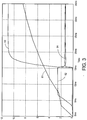
- FIGS. 3-5 show simulation results for hot swap device 31 under various operating conditions.
- FIG. 3 shows hot swap device 31 turning on into a nominal load of 2.5 amperes. Under these conditions, current is limited by load 44, not I DSAT .
- Curve 61 shows gate 48 of MOSFET device 41 slowly charging through a large Rg (e.g., 10 MOhms) and curve 62 (I ds for device 41) shows that the entire 2.5 amperes is first conducted entirely through first switch or MOSFET device 41 according to the present invention.
- comparator circuit 36 turns on second switch or MOSFET device 42 (curve 63, which shows V gs for device 42), and about 1.25 amperes is conducted through both MOSFET devices 41 (I ds curve 62) and 42 (I ds curve 64).
- MOSFET devices 41 I ds curve 62
- I ds curve 64 I ds curve 64
- both gates 48 and 49 fully charge to about 11 volts, and hot swap device 31 according to the present invention operates with a very low R DSon (e.g., less than about 35 Mohms).
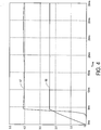
- FIG. 4 shows hot swap device 31 turning on under a shorted load condition.
- first switch or MOSFET device 41 is turned on to conduct current, which is limited at about 4 amperes (I ds curve 67).
- V gs curve 68 the gate voltage of first switch 41 charges to about 2.4 volts while first switch 41 is in current limit mode.
- second switch or MOSFET device 42 is not on during shorted load conditions.
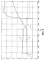
- FIG. 5 shows hot swap device 31 turning on into a large capacitive load 46 of 1000 uF with a load 44 of 2.5 amperes in parallel. Initially, these conditions appear as a shorted load until capacitor 46 is charged. The load then returns to a nominal 2.5 amperes.
- current in first switch 41 initially increases to 4 amperes, which corresponds a current limit mode according to the present invention. At about 27 milliseconds, capacitor 46 is charged, and the current drops to 2.5 amperes as shown by curve 71. At this time, only first switch 41 is turned on. At about 35 milliseconds, V gs of first switch 41 exceeds 5 volts as shown by V gs curve 72. At this point, second switch 42 turns on (V gs curve 73) according to the present invention, and current is then split between devices 41 and 42 at 1.25 amperes each as shown by I ds curves 71 and 74.
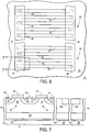
- FIG. 6 shows a highly enlarged partial top view of a split, multiple, divided, or separated gate structure 81 according to the present invention formed on a body of semiconductor material 84.
- Split gate structure 81 is shown with a first embodiment 82 and an alternative embodiment 83.
- a first gate feed 86 is coupled to a plurality of first control or gate electrodes 87
- a second gate feed 91 is coupled to a plurality of second control or gate electrodes 92.
- at least one of the second gate electrodes 92 is juxtaposed, next to, or adjacent to one of the first gate electrodes.
- at least one of the second gate electrodes 92 is interdigitated between a pair of first gate electrodes 87.
- more than one of second gate electrodes 92 is interdigitated between a pair of first gate electrodes 87.
- two gate electrodes 92 are shown in FIG. 6 between a pair of first gate electrodes 87, it is understood that more than two second gate electrodes 92 may be interditigated between a pair of first gate electrodes 87 depending on system requirements.
- FIG. 7 shows an enlarged cross-section view of hot swap device 31 including split gate structure 81 taken along reference line 6-6 in FIG. 1 .
- Hot swap device 31 preferably is formed on one body of semiconductor material 84 and includes split gate device 33, comparator device 36, and current limit device 38.
- Split gate device 33 includes a first pair of current carrying electrodes or regions 52 and 53, and a second pair of current carrying electrodes or regions 54 and 56.
- First gate or control electrode 87 is formed on body of semiconductor material 84, and controls first pair of current carrying electrodes 52 and 53.
- Second gate or control electrode 92 is formed on body of semiconductor material 84, and controls second pair of current carrying electrodes 54 and 56.
- current carrying electrodes 52 and 56 form source regions of device 33, and current electrodes 53 and 54 form drain regions.
- current carrying electrodes 53 and 54 are formed in the same portion of body of semiconductor material 84 to provide a common drain region 96.
- currently carrying electrodes 52, 53, 54, and 56 are formed in the same body of semiconductor material to provide an integrated device.
- current carrying electrodes or regions 52 and 56 are coupled together with a common electrode or contact 151, and current carrying electrodes or regions 53 and 54 are coupled together with a common electrode or contact 152.
- Comparator device 36 is formed in a region 361 of body of semiconductor material 84, and current limit device 38 is formed in a region 381.
- FIG. 8 shows a circuit diagram of a preferred current limit device or circuit 38 coupled to first switch 41.
- Resistor 106 and diode 107 set node V z preferably to about 5.5 volts.
- Resistors 101, 102, and 103 and switching device 109 set node V ref to (1+R 102 /R 103 )*V th (of device 109) by choosing specific values so that node V ref is a few tenths of a volt below V th of switching device 109.
- the current through the sense cells (i.e., switch 43) is routed through Rsense to develop a voltage Vsense.
- Vsense As Vsense increases, the voltage at the gate of switching device 41 increases, and eventually switching device 41 turns on through switch 111.
- Resistors 112 and 113 function as a level shift set the gate voltage of switch 11.
- Device 41 pulls current through resistor R G1 , which decreases the gate voltage thereby limiting current flow in first switch 41.
- a semiconductor switching device having low R DSon and a low current limit.
- the device includes a split gate structure that turns on a portion of the switching device during a current limit mode, and that turns on another portion of the switching device when non-current limit conditions are met.
- the present invention provides a device that overcomes thermal runaway problems associated with prior art switching devices.
Claims (8)
- Hot-Swap-Schutzvorrichtung, die eine Leistungsschaltvorrichtung und eine Steuerungsvorrichtung zum Steuern der Leistungsschaltvorrichtung umfasst, wobei die Leistungsschaltvorrichtung umfasst:eine erste Schaltvorrichtung (41) mit einer ersten Steuerungselektrode (48);eine zweite Schaltvorrichtung (42) mit einer zweiten Steuerungselektrode (49), die von der ersten Steuerungselektrode getrennt ist, wobei die erste und zweite Schaltvorrichtung (41, 42) als Teil eines einzigen Körpers aus Halbleitermaterial ausgebildet sind und wobei die erste und zweite Schaltvorrichtung (41, 42) eine gemeinsame Strom führende Elektrode (53, 54) zum Koppeln mit einer Last (44) aufweisen;gekennzeichnet durcheine Strombegrenzungsvorrichtung (38), die mit der ersten Steuerungselektrode gekoppelt ist, wobei die Strombegrenzungsvorrichtung und die Steuerungsvorrichtung ausgestaltet sind, um während eines Betriebsmodus mit Strombegrenzung nur die erste Schaltvorrichtung (41) einzuschalten; undeine Vergleichervorrichtung, die mit der ersten Steuerungselektrode und der zweiten Steuerungselektrode gekoppelt ist, wobei die Vergleichervorrichtung und die Steuerungsvorrichtung ausgestaltet sind, um die zweite Schaltvorrichtung (42) während eines Betriebsmodus ohne Strombegrenzung einzuschalten.
- Vorrichtung nach Anspruch 1,
wobei die Strombegrenzungsvorrichtung (38) als Teil des einzigen Körpers aus Halbleitermaterial ausgebildet ist. - Vorrichtung nach Anspruch 1,
wobei die Vergleichervorrichtung als Teil des einzigen Körpers aus Halbleitermaterial ausgebildet ist. - Vorrichtung nach Anspruch 1,
wobei die Vergleichervorrichtung (36) ausgestaltet ist, um die zweite Schaltvorrichtung (42) einzuschalten, wenn eine Steuerungsvorspannung an der ersten Steuerungselektrode (48) einen vorbestimmten Wert erreicht. - Vorrichtung nach Anspruch 1,
wobei die Steuerungsvorspannung etwa 5 Volt beträgt. - Vorrichtung nach Anspruch 1,
wobei die erste und zweite Steuerungselektrode (48, 49) eine ineinandergreifende Struktur umfassen. - Vorrichtung nach Anspruch 1,
wobei die ineinandergreifende Struktur mindestens ein Paar zweiter Steuerungselektroden zwischen einem Paar erster Steuerungselektroden umfasst. - Hot-Swap-Schutzvorrichtung nach Anspruch 1,
wobei die Leistungsschaltvorrichtung eine MOSFET-Vorrichtung umfasst.
Applications Claiming Priority (2)
| Application Number | Priority Date | Filing Date | Title |
|---|---|---|---|
| US10/678,769 US6949961B2 (en) | 2003-10-06 | 2003-10-06 | Power switch structure with low RDSon and low current limit |
| PCT/US2004/030143 WO2005041380A1 (en) | 2003-10-06 | 2004-09-15 | Power switch structure and method |
Publications (2)
| Publication Number | Publication Date |
|---|---|
| EP1671408A1 EP1671408A1 (de) | 2006-06-21 |
| EP1671408B1 true EP1671408B1 (de) | 2018-02-28 |
Family
ID=34394009
Family Applications (1)
| Application Number | Title | Priority Date | Filing Date |
|---|---|---|---|
| EP04784112.7A Expired - Fee Related EP1671408B1 (de) | 2003-10-06 | 2004-09-15 | Leistungsschalterstruktur und -verfahren |
Country Status (8)
| Country | Link |
|---|---|
| US (2) | US6949961B2 (de) |
| EP (1) | EP1671408B1 (de) |
| JP (2) | JP5179755B2 (de) |
| KR (1) | KR101099384B1 (de) |
| CN (1) | CN100557916C (de) |
| HK (1) | HK1095434A1 (de) |
| TW (1) | TWI368989B (de) |
| WO (1) | WO2005041380A1 (de) |
Families Citing this family (51)
| Publication number | Priority date | Publication date | Assignee | Title |
|---|---|---|---|---|
| US7230302B2 (en) * | 2004-01-29 | 2007-06-12 | Enpirion, Inc. | Laterally diffused metal oxide semiconductor device and method of forming the same |
| US8212316B2 (en) | 2004-01-29 | 2012-07-03 | Enpirion, Inc. | Integrated circuit with a laterally diffused metal oxide semiconductor device and method of forming the same |
| US8212315B2 (en) | 2004-01-29 | 2012-07-03 | Enpirion, Inc. | Integrated circuit with a laterally diffused metal oxide semiconductor device and method of forming the same |
| US8253197B2 (en) | 2004-01-29 | 2012-08-28 | Enpirion, Inc. | Integrated circuit with a laterally diffused metal oxide semiconductor device and method of forming the same |
| US8253196B2 (en) | 2004-01-29 | 2012-08-28 | Enpirion, Inc. | Integrated circuit with a laterally diffused metal oxide semiconductor device and method of forming the same |
| US8253195B2 (en) | 2004-01-29 | 2012-08-28 | Enpirion, Inc. | Integrated circuit with a laterally diffused metal oxide semiconductor device and method of forming the same |
| US8212317B2 (en) | 2004-01-29 | 2012-07-03 | Enpirion, Inc. | Integrated circuit with a laterally diffused metal oxide semiconductor device and method of forming the same |
| US7414335B2 (en) * | 2004-04-15 | 2008-08-19 | Seagate Technology | Inrush current controller |
| US7190026B2 (en) * | 2004-08-23 | 2007-03-13 | Enpirion, Inc. | Integrated circuit employable with a power converter |
| US7335948B2 (en) * | 2004-08-23 | 2008-02-26 | Enpirion, Inc. | Integrated circuit incorporating higher voltage devices and low voltage devices therein |
| US7015544B2 (en) * | 2004-08-23 | 2006-03-21 | Enpirion, Inc. | Intergrated circuit employable with a power converter |
| US7229886B2 (en) * | 2004-08-23 | 2007-06-12 | Enpirion, Inc. | Method of forming an integrated circuit incorporating higher voltage devices and low voltage devices therein |
| US7186606B2 (en) | 2004-08-23 | 2007-03-06 | Enpirion, Inc. | Method of forming an integrated circuit employable with a power converter |
| US7214985B2 (en) * | 2004-08-23 | 2007-05-08 | Enpirion, Inc. | Integrated circuit incorporating higher voltage devices and low voltage devices therein |
| US7195981B2 (en) | 2004-08-23 | 2007-03-27 | Enpirion, Inc. | Method of forming an integrated circuit employable with a power converter |
| US7232733B2 (en) * | 2004-08-23 | 2007-06-19 | Enpirion, Inc. | Method of forming an integrated circuit incorporating higher voltage devices and low voltage devices therein |
| JP4203464B2 (ja) * | 2004-11-18 | 2009-01-07 | パナソニック株式会社 | Dc−dcコンバータ |
| US7609499B2 (en) * | 2005-05-05 | 2009-10-27 | Seagate Technology Llc | Active current limiting circuit |
| US7332358B2 (en) * | 2005-06-30 | 2008-02-19 | Potentia Semiconductor Inc. | MOSFET temperature sensing |
| US20070126871A1 (en) * | 2005-12-06 | 2007-06-07 | Henninger Paul E Iii | Modular surveillance camera system with self-identification capability |
| US20070126872A1 (en) * | 2005-12-06 | 2007-06-07 | Michael Bolotine | Modular surveillance camera system |
| GB2455524B (en) | 2007-12-11 | 2010-04-07 | Wolfson Microelectronics Plc | Charge pump circuit and methods of operation thereof and portable audio apparatus including charge pump circuits |
| GB2467450B (en) * | 2007-12-11 | 2011-07-20 | Wolfson Microelectronics Plc | Drive circuit |
| US7760479B2 (en) * | 2008-04-09 | 2010-07-20 | Fairchild Semiconductor Corporation | Technique for combining in-rush current limiting and short circuit current limiting |
| US7683693B2 (en) * | 2008-04-10 | 2010-03-23 | Fairchild Semiconductor Corporation | Hot swap controller with zero loaded charge pump |
| US8050001B2 (en) * | 2008-08-07 | 2011-11-01 | Crucs Holdings, Llc | Timed electrical outlet and a method of operation thereof |
| US8174148B2 (en) * | 2008-08-07 | 2012-05-08 | Crucs Holdings, Llc | Controllable electrical outlet and a method of operation thereof |
| US8138933B2 (en) * | 2008-11-05 | 2012-03-20 | Crucs Holdings, Llc | Systems, methods, and apparatus for automatically disabling appliances in response to a smoke detector |
| CN102741280B (zh) | 2009-10-30 | 2015-12-02 | 诺维信生物制药丹麦公司 | 白蛋白变体 |
| CN102570809B (zh) * | 2010-12-31 | 2016-02-24 | 意法半导体研发(深圳)有限公司 | 短路保护电路及方法 |
| TWI492277B (zh) * | 2011-04-11 | 2015-07-11 | Great Power Semiconductor Corp | 具有快速切換能力之溝渠式功率金氧半導體結構之製造方法 |
| CN103166168B (zh) * | 2011-12-19 | 2016-11-02 | 上海航空电器有限公司 | 一种高压直流固态功率控制器 |
| US8766365B2 (en) * | 2012-02-21 | 2014-07-01 | Micron Technology, Inc. | Circuit-protection devices |
| JP5845108B2 (ja) | 2012-02-23 | 2016-01-20 | ルネサスエレクトロニクス株式会社 | パワーデバイス |
| AU2013234299B2 (en) | 2012-03-16 | 2017-06-22 | Albumedix Ltd. | Albumin variants |
| US9299691B2 (en) | 2012-11-30 | 2016-03-29 | Enpirion, Inc. | Semiconductor device including alternating source and drain regions, and respective source and drain metallic strips |
| US9536938B1 (en) | 2013-11-27 | 2017-01-03 | Altera Corporation | Semiconductor device including a resistor metallic layer and method of forming the same |
| US10020739B2 (en) | 2014-03-27 | 2018-07-10 | Altera Corporation | Integrated current replicator and method of operating the same |
| US9673192B1 (en) | 2013-11-27 | 2017-06-06 | Altera Corporation | Semiconductor device including a resistor metallic layer and method of forming the same |
| US10468917B2 (en) * | 2014-03-05 | 2019-11-05 | Ricoh Co., Ltd. | Battery charger |
| EP3130049B1 (de) | 2014-04-11 | 2021-07-28 | Telefonaktiebolaget LM Ericsson (publ) | Stromsteuerungsschaltung und verfahren dafür |
| JP6504429B2 (ja) * | 2014-12-08 | 2019-04-24 | 富士電機株式会社 | スイッチング電源装置 |
| US10103627B2 (en) | 2015-02-26 | 2018-10-16 | Altera Corporation | Packaged integrated circuit including a switch-mode regulator and method of forming the same |
| US10103724B2 (en) * | 2016-04-25 | 2018-10-16 | Infineon Technologies Ag | Dimension regulation of power device to eliminate hot spot generation |
| US10355132B2 (en) * | 2017-03-20 | 2019-07-16 | North Carolina State University | Power MOSFETs with superior high frequency figure-of-merit |
| US10361578B2 (en) * | 2017-05-10 | 2019-07-23 | Analog Devices, Inc. | Techniques for controlling current during power up in hot swap controllers |
| US10355656B2 (en) * | 2017-06-29 | 2019-07-16 | SK Hynix Inc. | Amplification circuit with split-length compensation scheme |
| EP3432455B1 (de) * | 2017-07-17 | 2022-11-09 | The Swatch Group Research and Development Ltd | Thermoelektrischer generator mit anlaufschaltung |
| US10163893B1 (en) | 2017-08-28 | 2018-12-25 | Micron Technologies, Inc. | Apparatus containing circuit-protection devices |
| US10431577B2 (en) | 2017-12-29 | 2019-10-01 | Micron Technology, Inc. | Methods of forming circuit-protection devices |
| US10903355B1 (en) | 2019-11-27 | 2021-01-26 | Analog Devices International Unlimited Company | Power switch arrangement |
Citations (1)
| Publication number | Priority date | Publication date | Assignee | Title |
|---|---|---|---|---|
| US20030169025A1 (en) * | 2002-01-25 | 2003-09-11 | Zetex Plc | Current limiting protection circuit |
Family Cites Families (22)
| Publication number | Priority date | Publication date | Assignee | Title |
|---|---|---|---|---|
| SE448333B (sv) * | 1982-02-18 | 1987-02-09 | Ericsson Telefon Ab L M | Elektronisk sekring ingaende i ett distributionssystem for likstrom |
| US5101313A (en) * | 1989-11-22 | 1992-03-31 | Tandem Computers Incorporated | System for protecting a dc power distribution bus during hot servicing |
| JPH05267580A (ja) * | 1992-03-24 | 1993-10-15 | Fuji Electric Co Ltd | 半導体装置 |
| JP2750986B2 (ja) * | 1992-10-27 | 1998-05-18 | 尚茂 玉蟲 | 分割ゲート型カソード短絡構造を有する絶縁ゲート静電誘導サイリスタ |
| JP2678159B2 (ja) * | 1992-11-06 | 1997-11-17 | 尚茂 玉蟲 | 分割ゲート型カソード短絡構造を有する絶縁ゲート静電誘導サイリスタ |
| JP3243902B2 (ja) * | 1993-09-17 | 2002-01-07 | 株式会社日立製作所 | 半導体装置 |
| KR0136531B1 (ko) * | 1994-07-08 | 1998-09-15 | 문정환 | 반도체장치의 제조방법 |
| JPH0832064A (ja) * | 1994-07-15 | 1996-02-02 | Fuji Electric Co Ltd | Mos半導体装置とその駆動方法および駆動回路 |
| JP3149773B2 (ja) * | 1996-03-18 | 2001-03-26 | 富士電機株式会社 | 電流制限回路を備えた絶縁ゲートバイポーラトランジスタ |
| JP3464340B2 (ja) * | 1996-04-19 | 2003-11-10 | 沖電気工業株式会社 | 半導体集積回路装置 |
| US5889303A (en) * | 1997-04-07 | 1999-03-30 | Motorola, Inc. | Split-Control gate electrically erasable programmable read only memory (EEPROM) cell |
| JP3077631B2 (ja) * | 1997-06-06 | 2000-08-14 | 日本電気株式会社 | 過熱保護機能付き電力駆動用mos型半導体素子 |
| US5986941A (en) * | 1997-10-09 | 1999-11-16 | Bright Microelectronics, Inc. | Programming current limiter for source-side injection EEPROM cells |
| US6043530A (en) * | 1998-04-15 | 2000-03-28 | Chang; Ming-Bing | Flash EEPROM device employing polysilicon sidewall spacer as an erase gate |
| JP3413569B2 (ja) * | 1998-09-16 | 2003-06-03 | 株式会社日立製作所 | 絶縁ゲート型半導体装置およびその製造方法 |
| JP2000101076A (ja) * | 1998-09-25 | 2000-04-07 | Toshiba Corp | 絶縁ゲート型半導体素子とその駆動方法 |
| DE19922924A1 (de) * | 1999-05-19 | 2000-11-30 | Siemens Ag | Überspannungsschutzvorrichtung für einen Halbleiterschalter |
| US6228718B1 (en) * | 1999-12-21 | 2001-05-08 | United Microelectronics Corp. | Method of fabricating a self-aligned split gate of a flash memory |
| US6400203B1 (en) * | 2000-08-07 | 2002-06-04 | Maxim Integrated Products, Inc. | Hot swap current limit circuits and methods |
| US6771478B2 (en) * | 2000-12-22 | 2004-08-03 | Ixys Corporation | Hot-swap protection circuit |
| US6515463B2 (en) | 2001-04-05 | 2003-02-04 | Semiconductor Components Industries Llc | Method and circuit for optimizing efficiency in a high frequency switching DC-DC converter |
| US6744094B2 (en) * | 2001-08-24 | 2004-06-01 | Micron Technology Inc. | Floating gate transistor with horizontal gate layers stacked next to vertical body |
-
2003
- 2003-10-06 US US10/678,769 patent/US6949961B2/en not_active Expired - Lifetime
-
2004
- 2004-09-15 EP EP04784112.7A patent/EP1671408B1/de not_active Expired - Fee Related
- 2004-09-15 KR KR1020067006616A patent/KR101099384B1/ko active IP Right Grant
- 2004-09-15 JP JP2006533923A patent/JP5179755B2/ja active Active
- 2004-09-15 CN CNB2004800290460A patent/CN100557916C/zh not_active Expired - Fee Related
- 2004-09-15 WO PCT/US2004/030143 patent/WO2005041380A1/en active Application Filing
- 2004-10-05 TW TW093130164A patent/TWI368989B/zh active
-
2005
- 2005-04-14 US US11/105,222 patent/US7230299B2/en not_active Expired - Lifetime
-
2007
- 2007-03-07 HK HK07102499.5A patent/HK1095434A1/xx not_active IP Right Cessation
-
2011
- 2011-02-22 JP JP2011035579A patent/JP5296119B2/ja active Active
Patent Citations (1)
| Publication number | Priority date | Publication date | Assignee | Title |
|---|---|---|---|---|
| US20030169025A1 (en) * | 2002-01-25 | 2003-09-11 | Zetex Plc | Current limiting protection circuit |
Also Published As
| Publication number | Publication date |
|---|---|
| US20050179084A1 (en) | 2005-08-18 |
| CN100557916C (zh) | 2009-11-04 |
| US7230299B2 (en) | 2007-06-12 |
| KR20060120654A (ko) | 2006-11-27 |
| TWI368989B (en) | 2012-07-21 |
| US6949961B2 (en) | 2005-09-27 |
| TW200520215A (en) | 2005-06-16 |
| US20050072987A1 (en) | 2005-04-07 |
| JP2007507893A (ja) | 2007-03-29 |
| JP5296119B2 (ja) | 2013-09-25 |
| JP2011135093A (ja) | 2011-07-07 |
| WO2005041380A1 (en) | 2005-05-06 |
| JP5179755B2 (ja) | 2013-04-10 |
| HK1095434A1 (en) | 2007-05-04 |
| EP1671408A1 (de) | 2006-06-21 |
| CN1864311A (zh) | 2006-11-15 |
| KR101099384B1 (ko) | 2011-12-29 |
Similar Documents
| Publication | Publication Date | Title |
|---|---|---|
| EP1671408B1 (de) | Leistungsschalterstruktur und -verfahren | |
| US7099135B2 (en) | Integrated inrush current limiter circuit and method | |
| US6865063B2 (en) | Integrated inrush current limiter circuit and method | |
| US5946177A (en) | Circuit for electrostatic discharge protection | |
| US7209332B2 (en) | Transient detection circuit | |
| US8233252B2 (en) | ESD protection circuit for low voltages | |
| US20030058593A1 (en) | Circuit configuration having a semiconductor switch and a protection circuit | |
| EP3605844B1 (de) | Schnelle überspannungs- und stosserkennung für hochgeschwindigkeits- und lastschalter | |
| US7126801B2 (en) | Polarity protection implemented with a MOSFET | |
| US6781502B1 (en) | Method of forming a protection circuit and structure therefor | |
| US5991175A (en) | Control circuit for an in-rush current control element, and a protection circuit and power supply employing the same | |
| US20080062730A1 (en) | Method and apparatus for distributing electrical power | |
| JPH02278915A (ja) | 電力用mosfetの保護回路 | |
| DE102017002573B4 (de) | Überspannungsschutz | |
| US6788506B1 (en) | Integrated circuit and method of operation | |
| US20060133001A1 (en) | Protection circuit | |
| CN217607483U (zh) | Esd保护电路、mcu芯片及bms芯片 | |
| CN111756242A (zh) | 相冗余方案中的or-fet本体制动 |
Legal Events
| Date | Code | Title | Description |
|---|---|---|---|
| PUAI | Public reference made under article 153(3) epc to a published international application that has entered the european phase |
Free format text: ORIGINAL CODE: 0009012 |
|
| AK | Designated contracting states |
Kind code of ref document: A1 Designated state(s): DE FR IT |
|
| 17P | Request for examination filed |
Effective date: 20060224 |
|
| DAX | Request for extension of the european patent (deleted) | ||
| RBV | Designated contracting states (corrected) |
Designated state(s): DE FR IT |
|
| 17Q | First examination report despatched |
Effective date: 20060920 |
|
| GRAP | Despatch of communication of intention to grant a patent |
Free format text: ORIGINAL CODE: EPIDOSNIGR1 |
|
| INTG | Intention to grant announced |
Effective date: 20170927 |
|
| GRAS | Grant fee paid |
Free format text: ORIGINAL CODE: EPIDOSNIGR3 |
|
| GRAA | (expected) grant |
Free format text: ORIGINAL CODE: 0009210 |
|
| AK | Designated contracting states |
Kind code of ref document: B1 Designated state(s): DE FR IT |
|
| REG | Reference to a national code |
Ref country code: DE Ref legal event code: R096 Ref document number: 602004052417 Country of ref document: DE |
|
| REG | Reference to a national code |
Ref country code: FR Ref legal event code: PLFP Year of fee payment: 15 |
|
| PG25 | Lapsed in a contracting state [announced via postgrant information from national office to epo] |
Ref country code: IT Free format text: LAPSE BECAUSE OF FAILURE TO SUBMIT A TRANSLATION OF THE DESCRIPTION OR TO PAY THE FEE WITHIN THE PRESCRIBED TIME-LIMIT Effective date: 20180228 |
|
| REG | Reference to a national code |
Ref country code: DE Ref legal event code: R097 Ref document number: 602004052417 Country of ref document: DE |
|
| PLBE | No opposition filed within time limit |
Free format text: ORIGINAL CODE: 0009261 |
|
| STAA | Information on the status of an ep patent application or granted ep patent |
Free format text: STATUS: NO OPPOSITION FILED WITHIN TIME LIMIT |
|
| 26N | No opposition filed |
Effective date: 20181129 |
|
| PGFP | Annual fee paid to national office [announced via postgrant information from national office to epo] |
Ref country code: FR Payment date: 20190820 Year of fee payment: 16 |
|
| PGFP | Annual fee paid to national office [announced via postgrant information from national office to epo] |
Ref country code: DE Payment date: 20200819 Year of fee payment: 17 |
|
| PG25 | Lapsed in a contracting state [announced via postgrant information from national office to epo] |
Ref country code: FR Free format text: LAPSE BECAUSE OF NON-PAYMENT OF DUE FEES Effective date: 20200930 |
|
| REG | Reference to a national code |
Ref country code: DE Ref legal event code: R119 Ref document number: 602004052417 Country of ref document: DE |
|
| PG25 | Lapsed in a contracting state [announced via postgrant information from national office to epo] |
Ref country code: DE Free format text: LAPSE BECAUSE OF NON-PAYMENT OF DUE FEES Effective date: 20220401 |