EP1614768A1 - Procede permettant de former un film - Google Patents
Procede permettant de former un film Download PDFInfo
- Publication number
- EP1614768A1 EP1614768A1 EP04710475A EP04710475A EP1614768A1 EP 1614768 A1 EP1614768 A1 EP 1614768A1 EP 04710475 A EP04710475 A EP 04710475A EP 04710475 A EP04710475 A EP 04710475A EP 1614768 A1 EP1614768 A1 EP 1614768A1
- Authority
- EP
- European Patent Office
- Prior art keywords
- gas
- metal
- film
- source gas
- during
- Prior art date
- Legal status (The legal status is an assumption and is not a legal conclusion. Google has not performed a legal analysis and makes no representation as to the accuracy of the status listed.)
- Withdrawn
Links
Images


Classifications
-
- C—CHEMISTRY; METALLURGY
- C23—COATING METALLIC MATERIAL; COATING MATERIAL WITH METALLIC MATERIAL; CHEMICAL SURFACE TREATMENT; DIFFUSION TREATMENT OF METALLIC MATERIAL; COATING BY VACUUM EVAPORATION, BY SPUTTERING, BY ION IMPLANTATION OR BY CHEMICAL VAPOUR DEPOSITION, IN GENERAL; INHIBITING CORROSION OF METALLIC MATERIAL OR INCRUSTATION IN GENERAL
- C23C—COATING METALLIC MATERIAL; COATING MATERIAL WITH METALLIC MATERIAL; SURFACE TREATMENT OF METALLIC MATERIAL BY DIFFUSION INTO THE SURFACE, BY CHEMICAL CONVERSION OR SUBSTITUTION; COATING BY VACUUM EVAPORATION, BY SPUTTERING, BY ION IMPLANTATION OR BY CHEMICAL VAPOUR DEPOSITION, IN GENERAL
- C23C16/00—Chemical coating by decomposition of gaseous compounds, without leaving reaction products of surface material in the coating, i.e. chemical vapour deposition [CVD] processes
- C23C16/44—Chemical coating by decomposition of gaseous compounds, without leaving reaction products of surface material in the coating, i.e. chemical vapour deposition [CVD] processes characterised by the method of coating
- C23C16/455—Chemical coating by decomposition of gaseous compounds, without leaving reaction products of surface material in the coating, i.e. chemical vapour deposition [CVD] processes characterised by the method of coating characterised by the method used for introducing gases into reaction chamber or for modifying gas flows in reaction chamber
- C23C16/45523—Pulsed gas flow or change of composition over time
-
- C—CHEMISTRY; METALLURGY
- C23—COATING METALLIC MATERIAL; COATING MATERIAL WITH METALLIC MATERIAL; CHEMICAL SURFACE TREATMENT; DIFFUSION TREATMENT OF METALLIC MATERIAL; COATING BY VACUUM EVAPORATION, BY SPUTTERING, BY ION IMPLANTATION OR BY CHEMICAL VAPOUR DEPOSITION, IN GENERAL; INHIBITING CORROSION OF METALLIC MATERIAL OR INCRUSTATION IN GENERAL
- C23C—COATING METALLIC MATERIAL; COATING MATERIAL WITH METALLIC MATERIAL; SURFACE TREATMENT OF METALLIC MATERIAL BY DIFFUSION INTO THE SURFACE, BY CHEMICAL CONVERSION OR SUBSTITUTION; COATING BY VACUUM EVAPORATION, BY SPUTTERING, BY ION IMPLANTATION OR BY CHEMICAL VAPOUR DEPOSITION, IN GENERAL
- C23C16/00—Chemical coating by decomposition of gaseous compounds, without leaving reaction products of surface material in the coating, i.e. chemical vapour deposition [CVD] processes
- C23C16/22—Chemical coating by decomposition of gaseous compounds, without leaving reaction products of surface material in the coating, i.e. chemical vapour deposition [CVD] processes characterised by the deposition of inorganic material, other than metallic material
- C23C16/30—Deposition of compounds, mixtures or solid solutions, e.g. borides, carbides, nitrides
- C23C16/34—Nitrides
-
- C—CHEMISTRY; METALLURGY
- C23—COATING METALLIC MATERIAL; COATING MATERIAL WITH METALLIC MATERIAL; CHEMICAL SURFACE TREATMENT; DIFFUSION TREATMENT OF METALLIC MATERIAL; COATING BY VACUUM EVAPORATION, BY SPUTTERING, BY ION IMPLANTATION OR BY CHEMICAL VAPOUR DEPOSITION, IN GENERAL; INHIBITING CORROSION OF METALLIC MATERIAL OR INCRUSTATION IN GENERAL
- C23C—COATING METALLIC MATERIAL; COATING MATERIAL WITH METALLIC MATERIAL; SURFACE TREATMENT OF METALLIC MATERIAL BY DIFFUSION INTO THE SURFACE, BY CHEMICAL CONVERSION OR SUBSTITUTION; COATING BY VACUUM EVAPORATION, BY SPUTTERING, BY ION IMPLANTATION OR BY CHEMICAL VAPOUR DEPOSITION, IN GENERAL
- C23C16/00—Chemical coating by decomposition of gaseous compounds, without leaving reaction products of surface material in the coating, i.e. chemical vapour deposition [CVD] processes
- C23C16/44—Chemical coating by decomposition of gaseous compounds, without leaving reaction products of surface material in the coating, i.e. chemical vapour deposition [CVD] processes characterised by the method of coating
- C23C16/4401—Means for minimising impurities, e.g. dust, moisture or residual gas, in the reaction chamber
-
- C—CHEMISTRY; METALLURGY
- C23—COATING METALLIC MATERIAL; COATING MATERIAL WITH METALLIC MATERIAL; CHEMICAL SURFACE TREATMENT; DIFFUSION TREATMENT OF METALLIC MATERIAL; COATING BY VACUUM EVAPORATION, BY SPUTTERING, BY ION IMPLANTATION OR BY CHEMICAL VAPOUR DEPOSITION, IN GENERAL; INHIBITING CORROSION OF METALLIC MATERIAL OR INCRUSTATION IN GENERAL
- C23C—COATING METALLIC MATERIAL; COATING MATERIAL WITH METALLIC MATERIAL; SURFACE TREATMENT OF METALLIC MATERIAL BY DIFFUSION INTO THE SURFACE, BY CHEMICAL CONVERSION OR SUBSTITUTION; COATING BY VACUUM EVAPORATION, BY SPUTTERING, BY ION IMPLANTATION OR BY CHEMICAL VAPOUR DEPOSITION, IN GENERAL
- C23C16/00—Chemical coating by decomposition of gaseous compounds, without leaving reaction products of surface material in the coating, i.e. chemical vapour deposition [CVD] processes
- C23C16/44—Chemical coating by decomposition of gaseous compounds, without leaving reaction products of surface material in the coating, i.e. chemical vapour deposition [CVD] processes characterised by the method of coating
- C23C16/52—Controlling or regulating the coating process
-
- H—ELECTRICITY
- H01—ELECTRIC ELEMENTS
- H01L—SEMICONDUCTOR DEVICES NOT COVERED BY CLASS H10
- H01L21/00—Processes or apparatus adapted for the manufacture or treatment of semiconductor or solid state devices or of parts thereof
- H01L21/02—Manufacture or treatment of semiconductor devices or of parts thereof
- H01L21/04—Manufacture or treatment of semiconductor devices or of parts thereof the devices having at least one potential-jump barrier or surface barrier, e.g. PN junction, depletion layer or carrier concentration layer
- H01L21/18—Manufacture or treatment of semiconductor devices or of parts thereof the devices having at least one potential-jump barrier or surface barrier, e.g. PN junction, depletion layer or carrier concentration layer the devices having semiconductor bodies comprising elements of Group IV of the Periodic System or AIIIBV compounds with or without impurities, e.g. doping materials
- H01L21/28—Manufacture of electrodes on semiconductor bodies using processes or apparatus not provided for in groups H01L21/20 - H01L21/268
- H01L21/283—Deposition of conductive or insulating materials for electrodes conducting electric current
- H01L21/285—Deposition of conductive or insulating materials for electrodes conducting electric current from a gas or vapour, e.g. condensation
- H01L21/28506—Deposition of conductive or insulating materials for electrodes conducting electric current from a gas or vapour, e.g. condensation of conductive layers
- H01L21/28512—Deposition of conductive or insulating materials for electrodes conducting electric current from a gas or vapour, e.g. condensation of conductive layers on semiconductor bodies comprising elements of Group IV of the Periodic System
- H01L21/28556—Deposition of conductive or insulating materials for electrodes conducting electric current from a gas or vapour, e.g. condensation of conductive layers on semiconductor bodies comprising elements of Group IV of the Periodic System by chemical means, e.g. CVD, LPCVD, PECVD, laser CVD
-
- H—ELECTRICITY
- H01—ELECTRIC ELEMENTS
- H01L—SEMICONDUCTOR DEVICES NOT COVERED BY CLASS H10
- H01L21/00—Processes or apparatus adapted for the manufacture or treatment of semiconductor or solid state devices or of parts thereof
- H01L21/70—Manufacture or treatment of devices consisting of a plurality of solid state components formed in or on a common substrate or of parts thereof; Manufacture of integrated circuit devices or of parts thereof
- H01L21/71—Manufacture of specific parts of devices defined in group H01L21/70
- H01L21/768—Applying interconnections to be used for carrying current between separate components within a device comprising conductors and dielectrics
- H01L21/76838—Applying interconnections to be used for carrying current between separate components within a device comprising conductors and dielectrics characterised by the formation and the after-treatment of the conductors
- H01L21/76841—Barrier, adhesion or liner layers
- H01L21/76843—Barrier, adhesion or liner layers formed in openings in a dielectric
Definitions
- the present invention relates to a film-forming method for depositing a metal-nitride film such as a TiN (Titanium nitride) film onto a surface of an object to be processed such as a semiconductor wafer.
- a metal-nitride film such as a TiN (Titanium nitride) film onto a surface of an object to be processed such as a semiconductor wafer.
- a circuitry is often composed by a multilevel interconnection structure in a semiconductor device in response to a request for recent enhanced density and enhanced integration.
- a technique for filling a contact hole, which is a connection part between a lower-layer device and an upper-layer aluminum wiring, and a via hole, which is a connection part between a lower-layer aluminum wiring and an upper-layer aluminum wiring, is important to provide an electrical connection therebetween.
- Sputter aluminum and CVD tungsten are generally used as the technique to fill the contact hole, the via hole and the like. Recently, there is a tendency that the CVD tungsten is mainly used because of a higher filling performance thereof.
- WF 6 gas which is one of process gases used in this process breaks into the Si substrate side so as to deteriorate electric properties and the like. This tendency is not preferable.
- a barrier metal layer is thinly formed all over the surface of a wafer including a surface inside the hole.
- a double-layer structure of Ti/TiN (titanium nitride) or a single-layer structure of TiN is generally used as a material of this barrier metal layer.
- Japanese Patent Laid-Open Publication (Kokai) No. Hei-6-89873 Japanese Patent Laid-Open Publication (Kokai) No. Hei-10-106974, "Decomposition Property of Methylhydrazine with Titanium Nitridation at Low Temperature” (P. 934-938, J. Electrochem. Soc., Vol. 142 no.3, March 1995), and so on.
- a film-forming gas for example, a TiCl 4 gas and a NH 3 gas are used. These gases are introduced continuously and synchronously for a predetermined time into a processing container in which a vacuum has been created. Then, a TiN film is deposited on a surface of a wafer by means of a thermal CVD (Chemical Vapor Deposition) at a predetermined process temperature. After the TiN film is formed, into the same processing container, only the NH 3 gas is introduced for a predetermined time without introducing the TiCl 4 gas (which is called "post flow of NH 3 gas"). Thus, Cl elements remaining in the TiN film are removed. The reason of conducting the post-flow step is that if any Cl element remains in the film, resistivity of the film may increase and/or corrosion thereof may occur.
- the TiN film when the above TiN film is formed, in order to improve throughput, the TiN film is formed at a relatively high process temperature, for example about 560 °C.
- a relatively high process temperature for example about 560 °C.
- the process temperature is relatively high like this, less micro cracks or the like may be generated in the deposited film.
- the inventor has found that micro cracks may be generated when a film thickness of the deposited TiN film is thickened over a certain degree.
- An object of the present invention is to provide a film-forming method of a metal-nitride film in which less micro cracks and less peeling off may occur even at a relatively high temperature.
- the present invention is a film-forming method of forming a metal-nitride film onto a surface of an object to be processed in a processing container in which a vacuum can be created, the film-forming method comprising: a step of continuously supplying an inert gas into a processing container set at a high film-forming temperature; a step of intermittently supplying a metal-source gas into the processing container, during the step of continuously supplying the inert gas; a step of supplying a nitrogen-including reduction gas into the processing container at the same time that the metal-source gas is supplied, during a supply term of the metal-source gas, during the step of intermittently supplying the metal-source gas; and a step of supplying the nitrogen-including reduction gas into the processing container for a term shorter than a non-supply term of the metal-source gas, during the non-supply term of the metal-source gas, during the step of intermittently supplying the metal-source gas; wherein a film thickness of the metal-nitride film formed during the one supply
- a metal-nitride film can be deposited whose chlorine density is low, whose resistivity is low, and in which fewer cracks may be generated.
- the high film-forming temperature is 500 °C to 700 °C.
- a second nitrogen-including reduction gas whose reducing power is greater than that of the nitrogen-including reduction gas, is adapted to be supplied at the same time that the nitrogen-including reduction gas is supplied.
- a plasma-assist gas is adapted to be supplied at the same time that the nitrogen-including reduction gas is supplied, so as to generate plasma.
- a reduction gas is adapted to be supplied at the same time that the plasma-assist gas is supplied.
- the present invention is a film-forming method of forming a metal-nitride film onto a surface of an object to be processed in a processing container in which a vacuum can be created, the film-forming method comprising: a step of continuously supplying an inert gas and a nitrogen-including reduction gas into a processing container set at a high film-forming temperature; and a step of intermittently supplying a metal-source gas into the processing container, during the step of continuously supplying the inert gas and the nitrogen-including reduction gas; wherein a film thickness of the metal-nitride film formed during the one supply term of the metal-source gas is not more than 60 nm.
- a metal-nitride film can be deposited whose chlorine density is low, whose resistivity is low, and in which fewer cracks may be generated.
- the high film-forming temperature is 500 °C to 700 °C.
- a second nitrogen-including reduction gas whose reducing power is greater than that of the nitrogen-including reduction gas, is adapted to be supplied into the processing container for a term shorter than a non-supply term of the metal-source gas, during the non-supply term of the metal-source gas, during the step of intermittently supplying the metal-source gas.
- a plasma-assist gas is adapted to be supplied into the processing container for a term shorter than a non-supply term of the metal-source gas, during the non-supply term of the metal-source gas, during the step of intermittently supplying the metal-source gas, so as to generate plasma.
- a reduction gas is adapted to be supplied at the same time that the plasma-assist gas is supplied.
- the present invention is a film-forming method of forming a metal-nitride film onto a surface of an object to be processed in a processing container in which a vacuum can be created, the film-forming method comprising: a step of continuously supplying an inert gas into a processing container set at a high film-forming temperature; a step of intermittently supplying a metal-source gas into the processing container, during the step of continuously supplying the inert gas; a step of supplying a nitrogen-including reduction gas into the processing container for a term shorter than a supply term of the metal-source gas, during the supply term of the metal-source gas, during the step of intermittently supplying the metal-source gas; and a step of supplying the nitrogen-including reduction gas into the processing container for a term shorter than a non-supply term of the metal-source gas, during the non-supply term of the metal-source gas, during the step of intermittently supplying the metal-source gas; wherein a film thickness of the metal-nitride film
- a metal-nitride film can be deposited whose chlorine density is low, whose resistivity is low, and in which fewer cracks may be generated.
- the high film-forming temperature is 500 °C to 700 °C.
- either the start or the stop of supplying the nitrogen-including reduction gas is set at the same time as either the start or the stop of supplying the metal-source gas.
- a second nitrogen-including reduction gas whose reducing power is greater than that of the nitrogen-including reduction gas, is adapted to be supplied at the same time that the nitrogen-including reduction gas is supplied.
- a plasma-assist gas is adapted to be supplied at the same time that the nitrogen-including reduction gas is supplied, so as to generate plasma.
- a reduction gas is adapted to be supplied at the same time that the plasma-assist gas is supplied.
- the present invention is a film-forming method of forming a metal-nitride film onto a surface of an object to be processed in a processing container in which a vacuum can be created, the film-forming method comprising: a step of continuously supplying an inert gas into a processing container set at a high film-forming temperature; a step of intermittently supplying a metal-source gas into the processing container, during the step of continuously supplying the inert gas; a step of supplying a nitrogen-including reduction gas into the processing container at the same time that the metal-source gas is supplied, during a supply term of the metal-source gas, during the step of intermittently supplying the metal-source gas; and a step of supplying a second nitrogen-including reduction gas, whose reducing power is greater than that of the nitrogen-including reduction gas, into the processing container for a term shorter than a non-supply term of the metal-source gas, during the non-supply term of the metal-source gas, during the step of intermittently supplying the metal-source
- a metal-nitride film can be deposited whose chlorine density is low, whose resistivity is low, and in which fewer cracks may be generated.
- the high film-forming temperature is 500 °C to 700 °C.
- the present invention is a film-forming method of forming a metal-nitride film onto a surface of an object to be processed in a processing container in which a vacuum can be created, the film-forming method comprising: a step of continuously supplying an inert gas into a processing container set at a high film-forming temperature; a step of intermittently supplying a metal-source gas into the processing container, during the step of continuously supplying the inert gas; a step of supplying a nitrogen-including reduction gas into the processing container at the same time that the metal-source gas is supplied, during a supply term of the metal-source gas, during the step of intermittently supplying the metal-source gas; and a step of supplying a plasma-assist gas into the processing container for a term shorter than a non-supply term of the metal-source gas and continuous to the next supply term of the metal-source gas, during the non-supply term of the metal-source gas, during the step of intermittently supplying the metal-source gas, so as to
- a metal-nitride film can be deposited whose chlorine density is low, whose resistivity is low, and in which fewer cracks may be generated.
- the high film-forming temperature is 500 °C to 700 °C.
- a reduction gas is adapted to be supplied at the same time that the plasma-assist gas is supplied.
- the metal-source gas is for example TiCl 4 gas
- the nitrogen-including reduction gas is for example NH 3 gas.
- a Ti layer has been formed as a base layer on the surface of the object to be processed, onto which the metal-nitride film is to be formed, and that a film thickness of the metal-nitride film formed during the one supply term of the metal-source gas is not more than 20 nm.
- the inert gas is for example N 2 gas.
- the inert gas is for example Ar gas.
- the second nitrogen-including reduction gas is for example any of hydrazine, monomethylhydrazine and dimethylhydrazine.
- Fig. 1 is a schematic cross sectional view showing an example of processing unit for carrying out a film-forming method according to the present invention
- Fig. 2 is a chart showing timings of supply of various gases in a first embodiment according to the present invention.
- the processing unit is a plasma CVD film-forming unit and the metal-nitride film is a TiN film.
- the plasma CVD film-forming unit may be also used as a thermal CVD film-forming unit if a high-frequency voltage is not applied thereto so that no plasma is generated.
- the plasma CVD film-forming unit 10 as a processing unit has a processing container 12 formed cylindrically and made of, for example, nickel or a nickel alloy.
- a ceiling part of the processing container 12 is provided with a showerhead 16, which has a large number of gas-jetting holes (ways) 14A, 14B in a lower surface thereof.
- a process gas such as a film-forming gas or the like can be introduced into a processing space S in the processing container 12.
- two gas spaces 17A, 17B are separately defined in the showerhead 16.
- the gas jetting holes 14A, 14B are respectively communicated with the gas spaces 17A, 17B.
- the two gases are adapted to be first mixed in the processing space S. This manner of supplying the gases is called "post mix".
- the whole showerhead 16 is made of an electric conductor such as nickel or a nickel alloy and thus serves as an upper electrode.
- An outside peripheral surface and an upper surface of the showerhead 16, which serves as the upper electrode, are entirely covered with an insulating member 18 such as quartz or alumina (Al 2 O 3 ).
- the showerhead 16 is fixed to the processing container 12 with an insulation state via the insulating member 18.
- sealing members 20 such as O-rings or the like are respectively interposed at connecting parts between the showerhead 16, the insulating member 18 and the processing container 12. Thus, airtightness in the processing container 12 can be maintained.
- a high-frequency electric power source 24 that generates a high-frequency electric voltage of for example 450 kHz is connected to the showerhead 16 via a matching circuit 22 and a open-close switch 23.
- the high-frequency electric voltage is applied to the showerhead 16, which is the upper electrode.
- the frequency of the high-frequency electric voltage is not limited to 450 kHz, but could be for example 13.56 MHz or the like.
- a gate valve 28 that can be opened and closed is provided at the port 26.
- a load-lock chamber or a transfer chamber or the like, not shown, can be connected to the gate valve 28.
- An exhausting port 30 is provided at a bottom of the processing container 12.
- An exhausting pipe 31 is connected to the exhausting port 30, a vacuum pump or the like, not shown, being provided on the way of the exhausting pipe 31.
- a vacuum can be created in the processing container 12.
- a stage 34 onto which a semiconductor wafer W as an object to be processed is placed, is provided via a column 32 from the bottom.
- the stage 34 serves as a lower electrode.
- plasma can be generated by means of the high-frequency electric voltage in the processing space S between the stage 34 as the lower electrode and the showerhead 16 as the upper electrode.
- the whole stage 34 is made of a ceramics such as AIN.
- a heater 36 which consists of for example a resistive element such as a molybdenum wire, is buried in the stage 34 in a predetermined pattern.
- a heater electric power source 38 is connected to the heater 36 via a wiring 37.
- an electrode body 40 which is for example a mesh of molybdenum wire, is buried in the stage 34 above the heater 36, so as to spread out in the whole in-plane (radial) directions of the stage 34.
- the electrode body 40 is grounded via a wiring 42.
- a high-frequency electric voltage as a bias voltage can be applied to the electric body 40.
- a plurality of pin-holes 44 that extend through vertically are formed in the stage 34.
- the connecting ring 46 is connected to an upper end of a protrudable rod 50, which extends through the bottom of the processing container in a vertically movable manner.
- the lower end of the protrudable rod 50 is connected to an air cylinder 52.
- each pushing-up pin 48 can protrude upward from an upper end of each pin-hole 44 and subside downward, when the wafer W is conveyed thereto or therefrom.
- An extendable bellows 54 is provided for a penetration part of the bottom of the processing container by the protrudable rod 50.
- the protrudable rod 50 can be vertically moved while maintaining the airtightness in the processing container 12.
- a focus ring 56 is provided at a peripheral portion of the stage 34 as the lower electrode so as to concentrate the plasma into the processing container S.
- the gas pipes 58A, 58B are connected to the ceiling part of the showerhead 16 so as to communicate with the gas spaces 17A, 17B, respectively.
- An N 2 gas or an Ar gas as an inert gas and/or a TiCl 4 gas as a metal source gas is adapted to be supplied through the gas pipe 58B together with a carrier gas (for example, N 2 gas).
- a carrier gas for example, N 2 gas.
- an NH 3 gas as a nitrogen-including reduction gas, an Ar gas as a plasma assist gas, an H 2 gas as a reduction gas and/or an MMH (monomethylhydrazine) gas as a second nitrogen-including reduction gas whose reducing power is greater than that of the NH 3 gas are adapted to be supplied through the gas pipe 58A.
- the high-frequency electric power source 24 for generating the plasma is provided, but a film-forming process can be also carried out by means of a mere thermal CVD without using plasma.
- a film-forming process by means of a thermal CVD can be carried out by a film-forming unit with for example a heating lamp.
- a TiN film is deposited by means of a thermal CVD.
- an N 2 gas (see Fig. 2(A)) is used as an inert gas
- a TiCl 4 gas (see Fig. 2(B)) is used as a metal source gas
- an NH 3 gas (see Fig. 2(C)) is used as a nitrogen-including reduction gas.
- the above gases are supplied in accordance with pulse-patterns in time, as shown in Fig. 2.
- the N 2 gas as the inert gas is continuously supplied, while the TiCl 4 gas as the metal source gas is intermittently supplied, and the NH 3 gas as the nitrogen-including reduction gas is supplied at the same time that the metal source gas is supplied and also during non-supply terms of the source gas for shorter terms than the non-supply terms.
- a term from a timing at which the TiCl 4 gas starts to be supplied to the next timing at which the TiCl 4 gas starts to be supplied is defined as one cycle.
- the term of the cycle is about 40 seconds.
- the term of the cycle is not limited thereto, but could be for example in a range of 10 to 60 seconds.
- a supply term T2 for which the TiCl 4 gas and the NH 3 gas are synchronously supplied is about 10 seconds
- a term T3 for which the NH 3 gas is solely supplied is about 10 seconds.
- the term T3 is set at a substantially center of the non-supply term T1 of the TiCl 4 gas.
- a process temperature is a relatively high temperature, for example within a range of 500 to 700 °C (as a wafer temperature), specifically for example 600 °C.
- a film thickness of the TiN film formed during one cycle is set not more than 60 nm, although it depends on the process temperature. This point is described later.
- the TiN film can have a low resistivity, and fewer cracks may occur in the TiN film.
- the process temperature is relatively high, high throughput may be maintained.
- a through hole or a contact hole is filled, as described above, it may be filled suitably and efficiently without generating cracks.
- the TiCl 4 gas and the NH 3 gas which are gases contributing to the film-forming, are completely removed.
- step coverage at step portions may be improved, and overhang of the TiN film at through holes, contact holes or via holes may be prevented.
- Fig. 3 is a graph showing a relationship between numbers of cycles of gas-supply and resistivities of TiN films.
- Fig. 4 is a graph showing a relationship between wafer temperatures and chlorine densities in TiN films.
- Fig. 3 shows dependence of resistivity of the TiN film on the number of cycles of gas-supply, when average total thickness of the formed TiN film is about 30 nm.
- the respective gas flow rates are controlled so that a film having a thickness of about 1.9 nm is deposited per one cycle.
- Fig. 4 shows dependence of chlorine density in the TiN film on wafer temperatures.
- chlorine density when the process temperature is lower, chlorine density is higher, which is not preferable. (When the process temperature is enhanced, chlorine density is decreased.)
- chlorine density was not more than about 1 %. That is, with respect to the chlorine density, it has been found that the present invention can achieve a very good result.
- the number of cycles was sixteen, and a thin film having a thickness of 30 nm was formed.
- a relationship between film thicknesses and resistivities (relating to existence of cracks) is explained for a case wherein a film of a desired thickness is deposited by one gas-supply (conventional case), and for another case wherein a film of a desired thickness is deposited by a plurality of cycles of gas-supply and gas-supply stop in accordance with the present invention.
- Fig. 5 is a graph showing the relationship between film thicknesses and resistivities.
- a thin film having a thickness of about 20 nm was formed.
- the process temperature was 600 °C for both cases.
- the resistivity is decreased temporarily, and increased from a bottom at a film thickness of about 55 nm. In an area more than 55 nm of the film thickness, cracks may be generated in the deposited film, so that the resistivity may be increased.
- the resistivity is decreased in turn. At least, the resistivity continues to be decreased to a point wherein the whole film thickness reaches about 160 nm. That is, it was confirmed that no crack may be generated.
- Fig. 6 is a graph showing temperature dependency of stresses with respect to film thicknesses.
- a TiN film is deposited by one gas-supply (conventional method)
- a TiN film is deposited by intermittently and repeatedly supplying a TiCl 4 gas and an NH 3 gas in accordance with the present invention.
- it may be thought that cracks may be generated at portions (areas A1) wherein the stress is rapidly decreased.
- the film thickness of the TiN film that causes crack generation is also increased in order of about 20 nm, about 60 nm, and about 80 nm.
- the process temperature is set higher than 700 °C, when a semiconductor integration circuit is manufactured, various types of base thin films or the like, which has already been formed in the previous step of the TiN-film forming step, may be thermally badly affected, which is not suitable. That is, the maximum value of a film thickness formed by one gas-supply (one cycle) is about 60 nm when the process temperature is 700 °C.
- the film thickness deposited by one supply of the TiCl 4 gas was not more than about 10 nm when the process temperature was 500 °C, not more than about 40 nm when the process temperature was 600 °C, and not more than about 60 nm when the process temperature was 700 °C.
- the minimum value of a film thickness formed by one gas-supply is preferably not less than about 30 nm, taking into consideration throughput, although crack generation is more inhibited as the film thickness is thinner.
- Fig. 7 is a chart showing timings of supply of various gases in the first variant of the first embodiment. The explanation of the same gases as in Fig. 2 is omitted.
- a TiN film is deposited by a thermal CVD by supplying a second nitrogen-including reduction gas, for example a monomethylhydrazine (MMH) gas (see Fig. 7(D)), in addition to the gas supplying manner of the first embodiment.
- a second nitrogen-including reduction gas for example a monomethylhydrazine (MMH) gas (see Fig. 7(D)
- the MMH gas as the second nitrogen-including reduction gas whose reducing power is greater than that of the nitrogen-including reduction gas is adapted to be supplied.
- nitiriding power can be improved when the gas is supplied.
- the chlorine density can be more reduced, so that a more complete TiN film can be formed.
- Fig. 8 is a chart showing timings of supply of various gases and timings of generation of plasma, in the second variant of the first embodiment. The explanation of the same gases as in Fig. 2 is omitted.
- a TiN film is deposited by a plasma CVD: by adding a plasma assist gas, for example an Ar gas (see Fig. 8(D)), so as to generate plasma; and at that time by adding a reduction gas, for example an H 2 gas (see Fig. 8(F)), if necessary; in addition to the gas supplying manner of the first embodiment.
- a plasma assist gas for example an Ar gas (see Fig. 8(D))
- a reduction gas for example an H 2 gas (see Fig. 8(F)
- the Ar gas as the plasma assist gas is supplied so as to generate the plasma.
- the Ar gas is supplied only while the NH 3 FLOW is conducted, and a high-frequency electric voltage is applied to the upper electrode 16 so as to generate the plasma.
- the high-frequency electric voltage can be applied to both the upper electrode 16 and the lower electrode 40.
- the H 2 gas as the reduction gas can be supplied so as to improve the nitriding power further more.
- Fig. 9 is a chart showing timings of supply of various gases in the second embodiment according to the present invention.
- an inert gas and a nitrogen-including reduction gas are continuously supplied, while a metal source gas is intermittently supplied. That is, an N 2 gas as the inert gas and an NH 3 gas as the nitrogen-including reduction gas are continuously supplied, while a TiCl 4 gas as the metal source gas is intermittently supplied in accordance with a pulse-pattern in time.
- a TiN film is deposited by a thermal CVD.
- a step cycle of DEPO ⁇ NH 3 FLOW (nitridation) ( ⁇ DEPO ⁇ NH 3 FLOW (nitridation)) ... is repeated in sequence.
- a supply term T2 and a non-supply term T1 of the TiCl 4 gas are set to substantially the same term.
- the term of the cycle is for example about 30 seconds.
- the TiN film can have a low resistivity, and fewer cracks may occur in the TiN film.
- the DEPO step for supplying the TiCl 4 gas and the nitriding step of the NH 3 FLOW are continuous (adjacent), that is, there is no N 2 PURGE step, differently from the first embodiment shown in Fig. 2.
- a state may be temporarily generated wherein density (partial pressure) of the TiCl 4 gas is extremely smaller than density (partial pressure) of the NH 3 gas, which is continuously supplied. This may act to deteriorate step coverage slightly.
- the N 2 PURGE step since the N 2 PURGE step is omitted, throughput may be enhanced.
- Fig. 10 is a chart showing timings of supply of various gases in the first variant of the second embodiment. The explanation of the same gases as in Fig. 9 is omitted.
- a TiN film is deposited by a thermal CVD by supplying a second nitrogen-including reduction gas, for example a monomethylhydrazine gas (see Fig. 10(D)), in addition to the gas supplying manner of the second embodiment.
- a second nitrogen-including reduction gas for example a monomethylhydrazine gas (see Fig. 10(D)
- the MMH gas as the second nitrogen-including reduction gas whose reducing power is greater than that of the NH 3 gas as the nitrogen-including reduction gas, is adapted to be supplied.
- nitiriding power can be improved when the gas is supplied.
- the chlorine density can be more reduced, so that a more complete TiN film can be formed.
- the supply term T4 of the MMH gas is set at substantially the center of the non-supply term T1 of the TiCl 4 gas.
- the supply timing of the TiCl 4 gas and the supply timing of the MMH gas are different from each other so that both the gases are not supplied at the same time. Thus, nitriding power may not be too great, and step coverage may not be deteriorated.
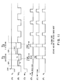
- Fig. 11 is a chart showing timings of supply of various gases and timings of generation of plasma, in the second variant of the second embodiment. The explanation of the same gases as in Fig. 9 is omitted.
- a TiN film is deposited by a plasma CVD: by adding a plasma assist gas, for example an Ar gas (see Fig. 11(D)), so as to generate plasma; and at that time by adding a reduction gas, for example an H 2 gas (see Fig. 11(F)), if necessary; in addition to the gas supplying manner of the second embodiment.
- a plasma assist gas for example an Ar gas (see Fig. 11(D))
- a reduction gas for example an H 2 gas (see Fig. 11(F)
- the Ar gas as the plasma assist gas is supplied so as to generate the plasma.
- the supply term T5 of the Ar gas is set at substantially the center of the non-supply term T1 of the TiCl 4 gas.
- the Ar gas is supplied, and a high-frequency electric voltage is applied to the upper electrode 16, so as to generate the plasma.
- nitriding power to the TiN film is further enhanced, and thus a more complete TiN film whose chlorine density is smaller can be formed.
- the H 2 gas as the reduction gas can be supplied so as to improve the nitriding power further more.
- the high-frequency electric voltage can be applied to both the upper electrode 16 and the lower electrode 40.
- Fig. 12 is a chart showing timings of supply of various gases in the third embodiment according to the present invention.
- an inert gas is continuously supplied, while a metal source gas is intermittently supplied.
- a nitrogen-including reduction gas is supplied during the supply terms T2 of the metal source gas, for terms T6 shorter than the supply terms T2, and also during the non-supply terms T1 of the metal source gas, for terms T3 shorter than the non-supply terms T1.
- an N 2 gas as the inert gas is continuously supplied, while a TiCl 4 gas as the metal source gas is intermittently supplied in accordance with a pulse-pattern in time.
- the NH 3 gas as the nitrogen-including reduction gas is supplied in accordance with a pulse-pattern in time, that is, for the terms T6 and T3 that are respectively shorter than the supply terms T2 and the non-supply terms T1 of the TiCl 4 gas, during the supply terms T2 and the non-supply terms T1 of the TiCl 4 gas. That is, there are a PRE-FLOW term and a POST-FLOW term of the TiCl 4 gas before and after the DEPO step.
- the supply term T6 of the NH 3 gas during the supply term T2 of the TiCl 4 gas is set at substantially the center of the supply term T2 of the TiCl 4 gas
- the supply term T3 of the NH 3 gas during the non-supply term T1 of the TiCl 4 gas is set at substantially the center of the non-supply term T1 of the TiCl 4 gas.
- the term of the cycle is for example about 15 to 70 seconds.
- the TiN film can have a low resistivity, and fewer cracks may occur in the TiN film.
- the PRE-FLOW step of the TiCl 4 gas and the POST-FLOW step of the TiCl 4 gas are provided before and after the DEPO step so that the flow rate of the TiCl 4 gas is stabilized.
- the N 2 PURGE steps are provided before and after the NH 3 FLOW (nitridation) step, so as to completely discharge redundant gases. Therefore, step coverage may be improved more.
- the timing at which the NH 3 gas (nitrogen-including reduction gas) starts to be supplied and the timing at which the TiCl 4 gas starts to be supplied may be set at the same time.
- the timing at which the NH 3 gas (nitrogen-including reduction gas) ceases to be supplied and the timing at which the TiCl 4 gas ceases to be supplied may be set at the same time.
- Fig. 15 is a chart showing timings of supply of various gases in the first variant of the third embodiment (including (i) and (ii)). The explanation of the same gases as in Fig. 12 is omitted. In addition, in Fig. 15, the timings of supply of various gases are shown on the basis of the timings shown in Fig. 12.
- a TiN film is deposited by a thermal CVD by supplying a second nitrogen-including reduction gas, for example a monomethylhydrazine gas (see Fig. 15(D)), in addition to the gas supplying manner of the third embodiment.
- a second nitrogen-including reduction gas for example a monomethylhydrazine gas (see Fig. 15(D)
- the MMH gas as the second nitrogen-including reduction gas whose reducing power is greater than that of the nitrogen-including reduction gas is adapted to be supplied.
- nitiriding power can be improved when the gas is supplied.
- the chlorine density can be more reduced, so that a more complete TiN film can be formed.
- Fig. 16 is a chart showing timings of supply of various gases and timings of generation of plasma, in the second variant of the third embodiment. The explanation of the same gases as in Fig. 12 is omitted. In addition, in Fig. 16, the timings of supply of various gases are shown on the basis of the timings shown in Fig. 12.
- a TiN film is deposited by a plasma CVD: by adding a plasma assist gas, for example an Ar gas (see Fig. 16(D)), so as to generate plasma; and at that time by adding a reduction gas, for example an H 2 gas (see Fig. 16(F)), if necessary; in addition to the gas supplying manner of the third embodiment.
- a plasma assist gas for example an Ar gas (see Fig. 16(D))
- a reduction gas for example an H 2 gas (see Fig. 16(F)
- the Ar gas as the plasma assist gas is supplied so as to generate the plasma.
- the Ar gas is supplied only while the NH 3 FLOW is conducted, and a high-frequency electric voltage is applied to the upper electrode 16 so as to generate the plasma.
- nitriding power to the TiN film is further enhanced, and thus a more complete TiN film whose chlorine density is smaller can be formed.
- the H 2 gas as the reduction gas can be supplied so as to improve the nitriding power further more.
- the high-frequency electric voltage can be applied to both the upper electrode 16 and the lower electrode 40.
- Fig. 17 is a chart showing timings of supply of various gases in the fourth embodiment according to the present invention.
- an inert gas is continuously supplied, a metal source gas is intermittently supplied, and a nitrogen-including reduction gas is supplied at the same time that the metal source gas is supplied.
- a second nitrogen-including reduction gas is supplied during non-supply terms of the metal source gas, for terms shorter than the non-supply terms.
- an N 2 gas as the inert gas is continuously supplied, while a TiCl 4 gas as the metal source gas and an NH 3 gas as the nitrogen-including reduction gas are synchronously and intermittently supplied in accordance with a pulse-pattern in time.
- a MMH gas as the second nitrogen-including reduction gas whose reducing power is greater than that of the NH 3 gas, is supplied.
- the TiN film is deposited by the thermal CVD. That is, the TiN film is nitrided when the MMH gas is supplied (reduction of the chlorine is carried out).
- the fourth embodiment is a gas supplying manner corresponding to that wherein the supply terms T3 of the NH 3 gas are removed from the first variant of the first embodiment shown in Fig. 7.
- the supply terms T3 in Fig. 7 correspond to the supply terms T8 of the MMH gas in Fig. 17.
- a step cycle of DEPO ⁇ N 2 PURGE ⁇ MMH FLOW (nitridation) ⁇ N 2 PURGE ( ⁇ DEPO ⁇ N 2 PURGE ⁇ MMH FLOW (nitridation)) ... is repeated in sequence.
- the TiN film can have a low resistivity, and fewer cracks may occur in the TiN film.
- the term of the cycle is for example about 10 to 60 seconds.
- Fig. 18 is a chart showing timings of supply of various gases and timings of generation of plasma, in the fifth embodiment according to the present invention.
- an inert gas is continuously supplied, a metal source gas is intermittently supplied, and a nitrogen-including reduction gas is supplied at the same time that the metal source gas is supplied.
- a plasma assist gas is supplied during non-supply terms of the metal source gas, for terms shorter than the non-supply terms and continuous to the next supply terms of the metal-source gas, so as to generate plasma.
- an N 2 gas as the inert gas is continuously supplied, while a TiCl 4 gas as the metal source gas and an NH 3 gas as the nitrogen-including reduction gas are synchronously and intermittently supplied in accordance with a pulse-pattern in time.
- an Ar gas as the plasma assist gas is added to generate the plasma (see Fig. 18(E)).
- a reduction gas for example an H 2 gas (see Fig. 18(F)
- a reduction gas for example an H 2 gas (see Fig. 18(F))
- a TiN film is deposited by a plasma CVD.
- the Ar gas when supplied, a high-frequency electric voltage is applied to the upper electrode 16 so as to generate the plasma.
- nitriding power to the TiN film is further enhanced, and thus a more complete TiN film whose chlorine density is smaller can be formed.
- the H 2 gas as the reduction gas can be supplied so as to improve the nitriding power further more.
- the high-frequency electric voltage can be applied to both the upper electrode 16 and the lower electrode 40.
- the TiN film can have a low resistivity, and fewer cracks may occur in the TiN film.
- the NH 3 gas is not supplied during the plasma nitriding step (term T9).
- the plasma nitridation is conducted by the N 2 purge gas, so that the DEPO step (term T2) can be immediately conducted without necessity to conduct any N 2 PURGE step for discharging the NH 3 gas just after the plasma nitriding step.
- throughput may be improved.
- the term of the cycle of the present embodiment is about 5 to 60 seconds.
- the MMH gas is used as the second nitrogen-including reduction gas whose reducing power is great.
- this invention is not limited thereto, but other gases such as hydrazine or dimethylhydrazine may be also used.
- a kind of base layer onto which the TiN film is formed is not explained.
- the base layer is a Ti film
- the TiN film formed thereon tends to peel off very easily.
- a film thickness of the TiN film to be formed by one cycle is much thinner than the above case, that is, 40 to 60 nm / cycle. Specifically, for example, it has to be reduced to a range of less than 20 nm / cycle.
- the reason is explained hereinafter.
- the TiCl 4 gas supplied during a deposition process of the TiN film lightly etches the Ti film, so that TiCl x is formed as a reaction byproduct.
- the reaction byproduct may not be evaporated sufficiently, but may partly remain on a surface of the Ti film. The remaining reaction byproduct facilitates the peeling off of the TiN film.
- the present invention if the supply and the stop of each gas are repeatedly conducted, the remaining reaction byproduct is completely nitrided. Thus, the peeling off of the TiN film is inhibited. Then, the nitriding process that is necessary in the conventional methods becomes unnecessary, so that the number of steps may be reduced.
- the base layer is the Ti layer
- a maximum film thickness by one cycle that can prevent peeling off also depends on a thickness of the total TiN film to be finally formed.
- a maximum film thickness by one cycle when a TiN film is deposited on a base layer consisting of a Ti layer in accordance with the present invention was evaluated in relation to a film thickness of the total TiN film to be formed.
- the evaluation result is explained.
- Fig. 19 is a table showing a relationship between film thicknesses of the total TiN film and film thicknesses formed by one cycle.
- the film thickness of the total TiN film was changed between 10 nm and 160 nm.
- the film thickness by one cycle was changed between 1.25 nm and 80 nm.
- the process temperature was about 650 °C.
- the sign " ⁇ " shows a case in which peeling off is not found, and hence which is good.
- the sign “ ⁇ ” shows a case in which peeling off is found, and hence which is not good.
- the sign “ ⁇ ” shows a case in which peeling off is not found, but the thin film consists of one layer. Herein, no crack was found in all the deposited films.
- the film thickness to be formed by one cycle is as thick as 10 to 20 nm.
- the maximum film thickness to be formed by one cycle is about 10 nm
- the maximum film thickness to be formed by one cycle is about 20 nm.
- the stress of the TiN film is also gradually reduced, so that the maximum film thickness to be formed by one cycle is gradually increased.
- the TiN film is formed as a metal-nitride film.
- this invention is not limited thereto, but applicable to cases for forming other metal-nitride films such as a WN film or a TaN film.
- the semiconductor wafer is taken as an example of the object to be processed.
- this invention is not limited thereto, but applicable to cases for processing a glass substrate, an LCD substrate, and the like.
Applications Claiming Priority (2)
| Application Number | Priority Date | Filing Date | Title |
|---|---|---|---|
| JP2003042897A JP4214795B2 (ja) | 2003-02-20 | 2003-02-20 | 成膜方法 |
| PCT/JP2004/001476 WO2004074543A1 (fr) | 2003-02-20 | 2004-02-12 | Procede permettant de former un film |
Publications (2)
| Publication Number | Publication Date |
|---|---|
| EP1614768A1 true EP1614768A1 (fr) | 2006-01-11 |
| EP1614768A4 EP1614768A4 (fr) | 2007-07-04 |
Family
ID=32905380
Family Applications (1)
| Application Number | Title | Priority Date | Filing Date |
|---|---|---|---|
| EP04710475A Withdrawn EP1614768A4 (fr) | 2003-02-20 | 2004-02-12 | Procede permettant de former un film |
Country Status (6)
| Country | Link |
|---|---|
| US (2) | US20060193980A1 (fr) |
| EP (1) | EP1614768A4 (fr) |
| JP (1) | JP4214795B2 (fr) |
| KR (1) | KR100704060B1 (fr) |
| CN (2) | CN101469413A (fr) |
| WO (1) | WO2004074543A1 (fr) |
Cited By (1)
| Publication number | Priority date | Publication date | Assignee | Title |
|---|---|---|---|---|
| EP1892752A4 (fr) * | 2005-05-23 | 2009-09-30 | Tokyo Electron Ltd | Procede de formation de film et support de stockage informatique |
Families Citing this family (192)
| Publication number | Priority date | Publication date | Assignee | Title |
|---|---|---|---|---|
| JP4178776B2 (ja) * | 2001-09-03 | 2008-11-12 | 東京エレクトロン株式会社 | 成膜方法 |
| US7966969B2 (en) | 2004-09-22 | 2011-06-28 | Asm International N.V. | Deposition of TiN films in a batch reactor |
| US7833906B2 (en) * | 2008-12-11 | 2010-11-16 | Asm International N.V. | Titanium silicon nitride deposition |
| WO2011055671A1 (fr) * | 2009-11-04 | 2011-05-12 | 東京エレクトロン株式会社 | Procédé de formation de couche et procédé de formation de condensateur |
| JP2011168881A (ja) * | 2010-01-25 | 2011-09-01 | Hitachi Kokusai Electric Inc | 半導体装置の製造方法及び基板処理装置 |
| KR101573733B1 (ko) * | 2010-11-29 | 2015-12-04 | 가부시키가이샤 히다치 고쿠사이 덴키 | 반도체 장치의 제조 방법, 기판 처리 방법 및 기판 처리 장치 |
| KR101205136B1 (ko) * | 2010-12-17 | 2012-11-26 | 에스케이하이닉스 주식회사 | 반도체 소자 및 그 형성 방법 |
| US20130023129A1 (en) | 2011-07-20 | 2013-01-24 | Asm America, Inc. | Pressure transmitter for a semiconductor processing environment |
| JP2013151722A (ja) * | 2012-01-25 | 2013-08-08 | Hitachi Kokusai Electric Inc | 半導体装置の製造方法 |
| US10714315B2 (en) | 2012-10-12 | 2020-07-14 | Asm Ip Holdings B.V. | Semiconductor reaction chamber showerhead |
| US20160376700A1 (en) | 2013-02-01 | 2016-12-29 | Asm Ip Holding B.V. | System for treatment of deposition reactor |
| US20140363903A1 (en) * | 2013-06-10 | 2014-12-11 | Tokyo Ohta Kogyo Co., Ltd. | Substrate treating apparatus and method of treating substrate |
| US10941490B2 (en) | 2014-10-07 | 2021-03-09 | Asm Ip Holding B.V. | Multiple temperature range susceptor, assembly, reactor and system including the susceptor, and methods of using the same |
| US10276355B2 (en) | 2015-03-12 | 2019-04-30 | Asm Ip Holding B.V. | Multi-zone reactor, system including the reactor, and method of using the same |
| US10458018B2 (en) | 2015-06-26 | 2019-10-29 | Asm Ip Holding B.V. | Structures including metal carbide material, devices including the structures, and methods of forming same |
| US10211308B2 (en) | 2015-10-21 | 2019-02-19 | Asm Ip Holding B.V. | NbMC layers |
| US11139308B2 (en) | 2015-12-29 | 2021-10-05 | Asm Ip Holding B.V. | Atomic layer deposition of III-V compounds to form V-NAND devices |
| US10529554B2 (en) | 2016-02-19 | 2020-01-07 | Asm Ip Holding B.V. | Method for forming silicon nitride film selectively on sidewalls or flat surfaces of trenches |
| US11453943B2 (en) | 2016-05-25 | 2022-09-27 | Asm Ip Holding B.V. | Method for forming carbon-containing silicon/metal oxide or nitride film by ALD using silicon precursor and hydrocarbon precursor |
| US9859151B1 (en) | 2016-07-08 | 2018-01-02 | Asm Ip Holding B.V. | Selective film deposition method to form air gaps |
| US10612137B2 (en) | 2016-07-08 | 2020-04-07 | Asm Ip Holdings B.V. | Organic reactants for atomic layer deposition |
| US9887082B1 (en) | 2016-07-28 | 2018-02-06 | Asm Ip Holding B.V. | Method and apparatus for filling a gap |
| US9812320B1 (en) | 2016-07-28 | 2017-11-07 | Asm Ip Holding B.V. | Method and apparatus for filling a gap |
| US11532757B2 (en) | 2016-10-27 | 2022-12-20 | Asm Ip Holding B.V. | Deposition of charge trapping layers |
| US10714350B2 (en) | 2016-11-01 | 2020-07-14 | ASM IP Holdings, B.V. | Methods for forming a transition metal niobium nitride film on a substrate by atomic layer deposition and related semiconductor device structures |
| KR102546317B1 (ko) | 2016-11-15 | 2023-06-21 | 에이에스엠 아이피 홀딩 비.브이. | 기체 공급 유닛 및 이를 포함하는 기판 처리 장치 |
| KR20180068582A (ko) | 2016-12-14 | 2018-06-22 | 에이에스엠 아이피 홀딩 비.브이. | 기판 처리 장치 |
| US11447861B2 (en) | 2016-12-15 | 2022-09-20 | Asm Ip Holding B.V. | Sequential infiltration synthesis apparatus and a method of forming a patterned structure |
| US11581186B2 (en) | 2016-12-15 | 2023-02-14 | Asm Ip Holding B.V. | Sequential infiltration synthesis apparatus |
| US10269558B2 (en) | 2016-12-22 | 2019-04-23 | Asm Ip Holding B.V. | Method of forming a structure on a substrate |
| US11390950B2 (en) | 2017-01-10 | 2022-07-19 | Asm Ip Holding B.V. | Reactor system and method to reduce residue buildup during a film deposition process |
| US10468261B2 (en) | 2017-02-15 | 2019-11-05 | Asm Ip Holding B.V. | Methods for forming a metallic film on a substrate by cyclical deposition and related semiconductor device structures |
| US10770286B2 (en) | 2017-05-08 | 2020-09-08 | Asm Ip Holdings B.V. | Methods for selectively forming a silicon nitride film on a substrate and related semiconductor device structures |
| US11306395B2 (en) | 2017-06-28 | 2022-04-19 | Asm Ip Holding B.V. | Methods for depositing a transition metal nitride film on a substrate by atomic layer deposition and related deposition apparatus |
| KR20190009245A (ko) | 2017-07-18 | 2019-01-28 | 에이에스엠 아이피 홀딩 비.브이. | 반도체 소자 구조물 형성 방법 및 관련된 반도체 소자 구조물 |
| US11374112B2 (en) | 2017-07-19 | 2022-06-28 | Asm Ip Holding B.V. | Method for depositing a group IV semiconductor and related semiconductor device structures |
| US10590535B2 (en) | 2017-07-26 | 2020-03-17 | Asm Ip Holdings B.V. | Chemical treatment, deposition and/or infiltration apparatus and method for using the same |
| US10692741B2 (en) | 2017-08-08 | 2020-06-23 | Asm Ip Holdings B.V. | Radiation shield |
| US10770336B2 (en) | 2017-08-08 | 2020-09-08 | Asm Ip Holding B.V. | Substrate lift mechanism and reactor including same |
| US11769682B2 (en) | 2017-08-09 | 2023-09-26 | Asm Ip Holding B.V. | Storage apparatus for storing cassettes for substrates and processing apparatus equipped therewith |
| US11830730B2 (en) | 2017-08-29 | 2023-11-28 | Asm Ip Holding B.V. | Layer forming method and apparatus |
| US11295980B2 (en) | 2017-08-30 | 2022-04-05 | Asm Ip Holding B.V. | Methods for depositing a molybdenum metal film over a dielectric surface of a substrate by a cyclical deposition process and related semiconductor device structures |
| US10658205B2 (en) | 2017-09-28 | 2020-05-19 | Asm Ip Holdings B.V. | Chemical dispensing apparatus and methods for dispensing a chemical to a reaction chamber |
| WO2019103610A1 (fr) | 2017-11-27 | 2019-05-31 | Asm Ip Holding B.V. | Appareil comprenant un mini-environnement propre |
| CN111316417B (zh) | 2017-11-27 | 2023-12-22 | 阿斯莫Ip控股公司 | 与批式炉偕同使用的用于储存晶圆匣的储存装置 |
| US10872771B2 (en) | 2018-01-16 | 2020-12-22 | Asm Ip Holding B. V. | Method for depositing a material film on a substrate within a reaction chamber by a cyclical deposition process and related device structures |
| WO2019142055A2 (fr) | 2018-01-19 | 2019-07-25 | Asm Ip Holding B.V. | Procédé de dépôt d'une couche de remplissage d'espace par dépôt assisté par plasma |
| TW202325889A (zh) | 2018-01-19 | 2023-07-01 | 荷蘭商Asm 智慧財產控股公司 | 沈積方法 |
| US11081345B2 (en) | 2018-02-06 | 2021-08-03 | Asm Ip Holding B.V. | Method of post-deposition treatment for silicon oxide film |
| EP3737779A1 (fr) | 2018-02-14 | 2020-11-18 | ASM IP Holding B.V. | Procédé de dépôt d'un film contenant du ruthénium sur un substrat par un processus de dépôt cyclique |
| US10896820B2 (en) | 2018-02-14 | 2021-01-19 | Asm Ip Holding B.V. | Method for depositing a ruthenium-containing film on a substrate by a cyclical deposition process |
| KR102636427B1 (ko) | 2018-02-20 | 2024-02-13 | 에이에스엠 아이피 홀딩 비.브이. | 기판 처리 방법 및 장치 |
| US10975470B2 (en) | 2018-02-23 | 2021-04-13 | Asm Ip Holding B.V. | Apparatus for detecting or monitoring for a chemical precursor in a high temperature environment |
| US11473195B2 (en) | 2018-03-01 | 2022-10-18 | Asm Ip Holding B.V. | Semiconductor processing apparatus and a method for processing a substrate |
| US11629406B2 (en) | 2018-03-09 | 2023-04-18 | Asm Ip Holding B.V. | Semiconductor processing apparatus comprising one or more pyrometers for measuring a temperature of a substrate during transfer of the substrate |
| KR102646467B1 (ko) | 2018-03-27 | 2024-03-11 | 에이에스엠 아이피 홀딩 비.브이. | 기판 상에 전극을 형성하는 방법 및 전극을 포함하는 반도체 소자 구조 |
| US11230766B2 (en) | 2018-03-29 | 2022-01-25 | Asm Ip Holding B.V. | Substrate processing apparatus and method |
| TWI811348B (zh) | 2018-05-08 | 2023-08-11 | 荷蘭商Asm 智慧財產控股公司 | 藉由循環沉積製程於基板上沉積氧化物膜之方法及相關裝置結構 |
| KR102596988B1 (ko) | 2018-05-28 | 2023-10-31 | 에이에스엠 아이피 홀딩 비.브이. | 기판 처리 방법 및 그에 의해 제조된 장치 |
| US11270899B2 (en) | 2018-06-04 | 2022-03-08 | Asm Ip Holding B.V. | Wafer handling chamber with moisture reduction |
| US11718913B2 (en) | 2018-06-04 | 2023-08-08 | Asm Ip Holding B.V. | Gas distribution system and reactor system including same |
| US11286562B2 (en) | 2018-06-08 | 2022-03-29 | Asm Ip Holding B.V. | Gas-phase chemical reactor and method of using same |
| US10797133B2 (en) | 2018-06-21 | 2020-10-06 | Asm Ip Holding B.V. | Method for depositing a phosphorus doped silicon arsenide film and related semiconductor device structures |
| KR102568797B1 (ko) | 2018-06-21 | 2023-08-21 | 에이에스엠 아이피 홀딩 비.브이. | 기판 처리 시스템 |
| JP2021529254A (ja) | 2018-06-27 | 2021-10-28 | エーエスエム・アイピー・ホールディング・ベー・フェー | 金属含有材料ならびに金属含有材料を含む膜および構造体を形成するための周期的堆積方法 |
| US11499222B2 (en) | 2018-06-27 | 2022-11-15 | Asm Ip Holding B.V. | Cyclic deposition methods for forming metal-containing material and films and structures including the metal-containing material |
| US10612136B2 (en) | 2018-06-29 | 2020-04-07 | ASM IP Holding, B.V. | Temperature-controlled flange and reactor system including same |
| US10755922B2 (en) | 2018-07-03 | 2020-08-25 | Asm Ip Holding B.V. | Method for depositing silicon-free carbon-containing film as gap-fill layer by pulse plasma-assisted deposition |
| US10388513B1 (en) | 2018-07-03 | 2019-08-20 | Asm Ip Holding B.V. | Method for depositing silicon-free carbon-containing film as gap-fill layer by pulse plasma-assisted deposition |
| US11430674B2 (en) | 2018-08-22 | 2022-08-30 | Asm Ip Holding B.V. | Sensor array, apparatus for dispensing a vapor phase reactant to a reaction chamber and related methods |
| US11024523B2 (en) | 2018-09-11 | 2021-06-01 | Asm Ip Holding B.V. | Substrate processing apparatus and method |
| KR20200030162A (ko) | 2018-09-11 | 2020-03-20 | 에이에스엠 아이피 홀딩 비.브이. | 박막 증착 방법 |
| CN110970344A (zh) | 2018-10-01 | 2020-04-07 | Asm Ip控股有限公司 | 衬底保持设备、包含所述设备的系统及其使用方法 |
| US11232963B2 (en) | 2018-10-03 | 2022-01-25 | Asm Ip Holding B.V. | Substrate processing apparatus and method |
| KR102592699B1 (ko) | 2018-10-08 | 2023-10-23 | 에이에스엠 아이피 홀딩 비.브이. | 기판 지지 유닛 및 이를 포함하는 박막 증착 장치와 기판 처리 장치 |
| KR102546322B1 (ko) | 2018-10-19 | 2023-06-21 | 에이에스엠 아이피 홀딩 비.브이. | 기판 처리 장치 및 기판 처리 방법 |
| KR102605121B1 (ko) | 2018-10-19 | 2023-11-23 | 에이에스엠 아이피 홀딩 비.브이. | 기판 처리 장치 및 기판 처리 방법 |
| US11087997B2 (en) | 2018-10-31 | 2021-08-10 | Asm Ip Holding B.V. | Substrate processing apparatus for processing substrates |
| KR20200051105A (ko) | 2018-11-02 | 2020-05-13 | 에이에스엠 아이피 홀딩 비.브이. | 기판 지지 유닛 및 이를 포함하는 기판 처리 장치 |
| US11572620B2 (en) | 2018-11-06 | 2023-02-07 | Asm Ip Holding B.V. | Methods for selectively depositing an amorphous silicon film on a substrate |
| US10818758B2 (en) | 2018-11-16 | 2020-10-27 | Asm Ip Holding B.V. | Methods for forming a metal silicate film on a substrate in a reaction chamber and related semiconductor device structures |
| US11217444B2 (en) | 2018-11-30 | 2022-01-04 | Asm Ip Holding B.V. | Method for forming an ultraviolet radiation responsive metal oxide-containing film |
| KR102636428B1 (ko) | 2018-12-04 | 2024-02-13 | 에이에스엠 아이피 홀딩 비.브이. | 기판 처리 장치를 세정하는 방법 |
| US11158513B2 (en) | 2018-12-13 | 2021-10-26 | Asm Ip Holding B.V. | Methods for forming a rhenium-containing film on a substrate by a cyclical deposition process and related semiconductor device structures |
| JP2020096183A (ja) | 2018-12-14 | 2020-06-18 | エーエスエム・アイピー・ホールディング・ベー・フェー | 窒化ガリウムの選択的堆積を用いてデバイス構造体を形成する方法及びそのためのシステム |
| TWI819180B (zh) | 2019-01-17 | 2023-10-21 | 荷蘭商Asm 智慧財產控股公司 | 藉由循環沈積製程於基板上形成含過渡金屬膜之方法 |
| KR20200091543A (ko) | 2019-01-22 | 2020-07-31 | 에이에스엠 아이피 홀딩 비.브이. | 기판 처리 장치 |
| JP2020136678A (ja) | 2019-02-20 | 2020-08-31 | エーエスエム・アイピー・ホールディング・ベー・フェー | 基材表面内に形成された凹部を充填するための方法および装置 |
| KR102626263B1 (ko) | 2019-02-20 | 2024-01-16 | 에이에스엠 아이피 홀딩 비.브이. | 처리 단계를 포함하는 주기적 증착 방법 및 이를 위한 장치 |
| TW202104632A (zh) | 2019-02-20 | 2021-02-01 | 荷蘭商Asm Ip私人控股有限公司 | 用來填充形成於基材表面內之凹部的循環沉積方法及設備 |
| US11482533B2 (en) | 2019-02-20 | 2022-10-25 | Asm Ip Holding B.V. | Apparatus and methods for plug fill deposition in 3-D NAND applications |
| TW202100794A (zh) | 2019-02-22 | 2021-01-01 | 荷蘭商Asm Ip私人控股有限公司 | 基材處理設備及處理基材之方法 |
| CN109911843B (zh) * | 2019-02-27 | 2021-08-24 | 上海华虹宏力半导体制造有限公司 | 金属薄膜图形的制造方法 |
| US11742198B2 (en) | 2019-03-08 | 2023-08-29 | Asm Ip Holding B.V. | Structure including SiOCN layer and method of forming same |
| KR20200108242A (ko) | 2019-03-08 | 2020-09-17 | 에이에스엠 아이피 홀딩 비.브이. | 실리콘 질화물 층을 선택적으로 증착하는 방법, 및 선택적으로 증착된 실리콘 질화물 층을 포함하는 구조체 |
| JP2020167398A (ja) | 2019-03-28 | 2020-10-08 | エーエスエム・アイピー・ホールディング・ベー・フェー | ドアオープナーおよびドアオープナーが提供される基材処理装置 |
| KR20200116855A (ko) | 2019-04-01 | 2020-10-13 | 에이에스엠 아이피 홀딩 비.브이. | 반도체 소자를 제조하는 방법 |
| US11447864B2 (en) | 2019-04-19 | 2022-09-20 | Asm Ip Holding B.V. | Layer forming method and apparatus |
| KR20200125453A (ko) | 2019-04-24 | 2020-11-04 | 에이에스엠 아이피 홀딩 비.브이. | 기상 반응기 시스템 및 이를 사용하는 방법 |
| KR20200130121A (ko) | 2019-05-07 | 2020-11-18 | 에이에스엠 아이피 홀딩 비.브이. | 딥 튜브가 있는 화학물질 공급원 용기 |
| KR20200130118A (ko) | 2019-05-07 | 2020-11-18 | 에이에스엠 아이피 홀딩 비.브이. | 비정질 탄소 중합체 막을 개질하는 방법 |
| KR20200130652A (ko) | 2019-05-10 | 2020-11-19 | 에이에스엠 아이피 홀딩 비.브이. | 표면 상에 재료를 증착하는 방법 및 본 방법에 따라 형성된 구조 |
| JP2020188255A (ja) | 2019-05-16 | 2020-11-19 | エーエスエム アイピー ホールディング ビー.ブイ. | ウェハボートハンドリング装置、縦型バッチ炉および方法 |
| USD947913S1 (en) | 2019-05-17 | 2022-04-05 | Asm Ip Holding B.V. | Susceptor shaft |
| USD975665S1 (en) | 2019-05-17 | 2023-01-17 | Asm Ip Holding B.V. | Susceptor shaft |
| KR20200141002A (ko) | 2019-06-06 | 2020-12-17 | 에이에스엠 아이피 홀딩 비.브이. | 배기 가스 분석을 포함한 기상 반응기 시스템을 사용하는 방법 |
| KR20200143254A (ko) | 2019-06-11 | 2020-12-23 | 에이에스엠 아이피 홀딩 비.브이. | 개질 가스를 사용하여 전자 구조를 형성하는 방법, 상기 방법을 수행하기 위한 시스템, 및 상기 방법을 사용하여 형성되는 구조 |
| USD944946S1 (en) | 2019-06-14 | 2022-03-01 | Asm Ip Holding B.V. | Shower plate |
| KR20210005515A (ko) | 2019-07-03 | 2021-01-14 | 에이에스엠 아이피 홀딩 비.브이. | 기판 처리 장치용 온도 제어 조립체 및 이를 사용하는 방법 |
| JP2021015791A (ja) | 2019-07-09 | 2021-02-12 | エーエスエム アイピー ホールディング ビー.ブイ. | 同軸導波管を用いたプラズマ装置、基板処理方法 |
| CN112216646A (zh) | 2019-07-10 | 2021-01-12 | Asm Ip私人控股有限公司 | 基板支撑组件及包括其的基板处理装置 |
| KR20210010307A (ko) | 2019-07-16 | 2021-01-27 | 에이에스엠 아이피 홀딩 비.브이. | 기판 처리 장치 |
| KR20210010816A (ko) | 2019-07-17 | 2021-01-28 | 에이에스엠 아이피 홀딩 비.브이. | 라디칼 보조 점화 플라즈마 시스템 및 방법 |
| KR20210010820A (ko) | 2019-07-17 | 2021-01-28 | 에이에스엠 아이피 홀딩 비.브이. | 실리콘 게르마늄 구조를 형성하는 방법 |
| US11643724B2 (en) | 2019-07-18 | 2023-05-09 | Asm Ip Holding B.V. | Method of forming structures using a neutral beam |
| JP2021019198A (ja) | 2019-07-19 | 2021-02-15 | エーエスエム・アイピー・ホールディング・ベー・フェー | トポロジー制御されたアモルファスカーボンポリマー膜の形成方法 |
| CN112309843A (zh) | 2019-07-29 | 2021-02-02 | Asm Ip私人控股有限公司 | 实现高掺杂剂掺入的选择性沉积方法 |
| CN112309899A (zh) | 2019-07-30 | 2021-02-02 | Asm Ip私人控股有限公司 | 基板处理设备 |
| CN112309900A (zh) | 2019-07-30 | 2021-02-02 | Asm Ip私人控股有限公司 | 基板处理设备 |
| US11587815B2 (en) | 2019-07-31 | 2023-02-21 | Asm Ip Holding B.V. | Vertical batch furnace assembly |
| US11227782B2 (en) | 2019-07-31 | 2022-01-18 | Asm Ip Holding B.V. | Vertical batch furnace assembly |
| US11587814B2 (en) | 2019-07-31 | 2023-02-21 | Asm Ip Holding B.V. | Vertical batch furnace assembly |
| KR20210018759A (ko) | 2019-08-05 | 2021-02-18 | 에이에스엠 아이피 홀딩 비.브이. | 화학물질 공급원 용기를 위한 액체 레벨 센서 |
| USD965524S1 (en) | 2019-08-19 | 2022-10-04 | Asm Ip Holding B.V. | Susceptor support |
| USD965044S1 (en) | 2019-08-19 | 2022-09-27 | Asm Ip Holding B.V. | Susceptor shaft |
| JP2021031769A (ja) | 2019-08-21 | 2021-03-01 | エーエスエム アイピー ホールディング ビー.ブイ. | 成膜原料混合ガス生成装置及び成膜装置 |
| KR20210024423A (ko) | 2019-08-22 | 2021-03-05 | 에이에스엠 아이피 홀딩 비.브이. | 홀을 구비한 구조체를 형성하기 위한 방법 |
| USD940837S1 (en) | 2019-08-22 | 2022-01-11 | Asm Ip Holding B.V. | Electrode |
| USD979506S1 (en) | 2019-08-22 | 2023-02-28 | Asm Ip Holding B.V. | Insulator |
| USD949319S1 (en) | 2019-08-22 | 2022-04-19 | Asm Ip Holding B.V. | Exhaust duct |
| US11286558B2 (en) | 2019-08-23 | 2022-03-29 | Asm Ip Holding B.V. | Methods for depositing a molybdenum nitride film on a surface of a substrate by a cyclical deposition process and related semiconductor device structures including a molybdenum nitride film |
| KR20210024420A (ko) | 2019-08-23 | 2021-03-05 | 에이에스엠 아이피 홀딩 비.브이. | 비스(디에틸아미노)실란을 사용하여 peald에 의해 개선된 품질을 갖는 실리콘 산화물 막을 증착하기 위한 방법 |
| KR20210029090A (ko) | 2019-09-04 | 2021-03-15 | 에이에스엠 아이피 홀딩 비.브이. | 희생 캡핑 층을 이용한 선택적 증착 방법 |
| KR20210029663A (ko) | 2019-09-05 | 2021-03-16 | 에이에스엠 아이피 홀딩 비.브이. | 기판 처리 장치 |
| US11562901B2 (en) | 2019-09-25 | 2023-01-24 | Asm Ip Holding B.V. | Substrate processing method |
| CN112593212B (zh) | 2019-10-02 | 2023-12-22 | Asm Ip私人控股有限公司 | 通过循环等离子体增强沉积工艺形成拓扑选择性氧化硅膜的方法 |
| TW202129060A (zh) | 2019-10-08 | 2021-08-01 | 荷蘭商Asm Ip控股公司 | 基板處理裝置、及基板處理方法 |
| TW202115273A (zh) | 2019-10-10 | 2021-04-16 | 荷蘭商Asm Ip私人控股有限公司 | 形成光阻底層之方法及包括光阻底層之結構 |
| KR20210045930A (ko) | 2019-10-16 | 2021-04-27 | 에이에스엠 아이피 홀딩 비.브이. | 실리콘 산화물의 토폴로지-선택적 막의 형성 방법 |
| US11637014B2 (en) | 2019-10-17 | 2023-04-25 | Asm Ip Holding B.V. | Methods for selective deposition of doped semiconductor material |
| KR20210047808A (ko) | 2019-10-21 | 2021-04-30 | 에이에스엠 아이피 홀딩 비.브이. | 막을 선택적으로 에칭하기 위한 장치 및 방법 |
| US11646205B2 (en) | 2019-10-29 | 2023-05-09 | Asm Ip Holding B.V. | Methods of selectively forming n-type doped material on a surface, systems for selectively forming n-type doped material, and structures formed using same |
| KR20210054983A (ko) | 2019-11-05 | 2021-05-14 | 에이에스엠 아이피 홀딩 비.브이. | 도핑된 반도체 층을 갖는 구조체 및 이를 형성하기 위한 방법 및 시스템 |
| US11501968B2 (en) | 2019-11-15 | 2022-11-15 | Asm Ip Holding B.V. | Method for providing a semiconductor device with silicon filled gaps |
| KR20210062561A (ko) | 2019-11-20 | 2021-05-31 | 에이에스엠 아이피 홀딩 비.브이. | 기판의 표면 상에 탄소 함유 물질을 증착하는 방법, 상기 방법을 사용하여 형성된 구조물, 및 상기 구조물을 형성하기 위한 시스템 |
| CN112951697A (zh) | 2019-11-26 | 2021-06-11 | Asm Ip私人控股有限公司 | 基板处理设备 |
| KR20210065848A (ko) | 2019-11-26 | 2021-06-04 | 에이에스엠 아이피 홀딩 비.브이. | 제1 유전체 표면과 제2 금속성 표면을 포함한 기판 상에 타겟 막을 선택적으로 형성하기 위한 방법 |
| CN112885692A (zh) | 2019-11-29 | 2021-06-01 | Asm Ip私人控股有限公司 | 基板处理设备 |
| CN112885693A (zh) | 2019-11-29 | 2021-06-01 | Asm Ip私人控股有限公司 | 基板处理设备 |
| JP2021090042A (ja) | 2019-12-02 | 2021-06-10 | エーエスエム アイピー ホールディング ビー.ブイ. | 基板処理装置、基板処理方法 |
| KR20210070898A (ko) | 2019-12-04 | 2021-06-15 | 에이에스엠 아이피 홀딩 비.브이. | 기판 처리 장치 |
| TW202125596A (zh) | 2019-12-17 | 2021-07-01 | 荷蘭商Asm Ip私人控股有限公司 | 形成氮化釩層之方法以及包括該氮化釩層之結構 |
| US11527403B2 (en) | 2019-12-19 | 2022-12-13 | Asm Ip Holding B.V. | Methods for filling a gap feature on a substrate surface and related semiconductor structures |
| KR20210095050A (ko) | 2020-01-20 | 2021-07-30 | 에이에스엠 아이피 홀딩 비.브이. | 박막 형성 방법 및 박막 표면 개질 방법 |
| TW202130846A (zh) | 2020-02-03 | 2021-08-16 | 荷蘭商Asm Ip私人控股有限公司 | 形成包括釩或銦層的結構之方法 |
| KR20210100010A (ko) | 2020-02-04 | 2021-08-13 | 에이에스엠 아이피 홀딩 비.브이. | 대형 물품의 투과율 측정을 위한 방법 및 장치 |
| US11776846B2 (en) | 2020-02-07 | 2023-10-03 | Asm Ip Holding B.V. | Methods for depositing gap filling fluids and related systems and devices |
| US11781243B2 (en) | 2020-02-17 | 2023-10-10 | Asm Ip Holding B.V. | Method for depositing low temperature phosphorous-doped silicon |
| KR20210116240A (ko) | 2020-03-11 | 2021-09-27 | 에이에스엠 아이피 홀딩 비.브이. | 조절성 접합부를 갖는 기판 핸들링 장치 |
| US11876356B2 (en) | 2020-03-11 | 2024-01-16 | Asm Ip Holding B.V. | Lockout tagout assembly and system and method of using same |
| CN113394086A (zh) | 2020-03-12 | 2021-09-14 | Asm Ip私人控股有限公司 | 用于制造具有目标拓扑轮廓的层结构的方法 |
| KR20210124042A (ko) | 2020-04-02 | 2021-10-14 | 에이에스엠 아이피 홀딩 비.브이. | 박막 형성 방법 |
| TW202146689A (zh) | 2020-04-03 | 2021-12-16 | 荷蘭商Asm Ip控股公司 | 阻障層形成方法及半導體裝置的製造方法 |
| TW202145344A (zh) | 2020-04-08 | 2021-12-01 | 荷蘭商Asm Ip私人控股有限公司 | 用於選擇性蝕刻氧化矽膜之設備及方法 |
| US11821078B2 (en) | 2020-04-15 | 2023-11-21 | Asm Ip Holding B.V. | Method for forming precoat film and method for forming silicon-containing film |
| KR20210132605A (ko) | 2020-04-24 | 2021-11-04 | 에이에스엠 아이피 홀딩 비.브이. | 냉각 가스 공급부를 포함한 수직형 배치 퍼니스 어셈블리 |
| KR20210132600A (ko) | 2020-04-24 | 2021-11-04 | 에이에스엠 아이피 홀딩 비.브이. | 바나듐, 질소 및 추가 원소를 포함한 층을 증착하기 위한 방법 및 시스템 |
| TW202140831A (zh) | 2020-04-24 | 2021-11-01 | 荷蘭商Asm Ip私人控股有限公司 | 形成含氮化釩層及包含該層的結構之方法 |
| KR20210134226A (ko) | 2020-04-29 | 2021-11-09 | 에이에스엠 아이피 홀딩 비.브이. | 고체 소스 전구체 용기 |
| KR20210134869A (ko) | 2020-05-01 | 2021-11-11 | 에이에스엠 아이피 홀딩 비.브이. | Foup 핸들러를 이용한 foup의 빠른 교환 |
| KR20210141379A (ko) | 2020-05-13 | 2021-11-23 | 에이에스엠 아이피 홀딩 비.브이. | 반응기 시스템용 레이저 정렬 고정구 |
| KR20210143653A (ko) | 2020-05-19 | 2021-11-29 | 에이에스엠 아이피 홀딩 비.브이. | 기판 처리 장치 |
| KR20210145078A (ko) | 2020-05-21 | 2021-12-01 | 에이에스엠 아이피 홀딩 비.브이. | 다수의 탄소 층을 포함한 구조체 및 이를 형성하고 사용하는 방법 |
| TW202201602A (zh) | 2020-05-29 | 2022-01-01 | 荷蘭商Asm Ip私人控股有限公司 | 基板處理方法 |
| TW202218133A (zh) | 2020-06-24 | 2022-05-01 | 荷蘭商Asm Ip私人控股有限公司 | 形成含矽層之方法 |
| TW202217953A (zh) | 2020-06-30 | 2022-05-01 | 荷蘭商Asm Ip私人控股有限公司 | 基板處理方法 |
| KR20220010438A (ko) | 2020-07-17 | 2022-01-25 | 에이에스엠 아이피 홀딩 비.브이. | 포토리소그래피에 사용하기 위한 구조체 및 방법 |
| TW202204662A (zh) | 2020-07-20 | 2022-02-01 | 荷蘭商Asm Ip私人控股有限公司 | 用於沉積鉬層之方法及系統 |
| KR20220027026A (ko) | 2020-08-26 | 2022-03-07 | 에이에스엠 아이피 홀딩 비.브이. | 금속 실리콘 산화물 및 금속 실리콘 산질화물 층을 형성하기 위한 방법 및 시스템 |
| USD990534S1 (en) | 2020-09-11 | 2023-06-27 | Asm Ip Holding B.V. | Weighted lift pin |
| USD1012873S1 (en) | 2020-09-24 | 2024-01-30 | Asm Ip Holding B.V. | Electrode for semiconductor processing apparatus |
| TW202229613A (zh) | 2020-10-14 | 2022-08-01 | 荷蘭商Asm Ip私人控股有限公司 | 於階梯式結構上沉積材料的方法 |
| KR20220053482A (ko) | 2020-10-22 | 2022-04-29 | 에이에스엠 아이피 홀딩 비.브이. | 바나듐 금속을 증착하는 방법, 구조체, 소자 및 증착 어셈블리 |
| TW202223136A (zh) | 2020-10-28 | 2022-06-16 | 荷蘭商Asm Ip私人控股有限公司 | 用於在基板上形成層之方法、及半導體處理系統 |
| KR20220076343A (ko) | 2020-11-30 | 2022-06-08 | 에이에스엠 아이피 홀딩 비.브이. | 기판 처리 장치의 반응 챔버 내에 배열되도록 구성된 인젝터 |
| US11946137B2 (en) | 2020-12-16 | 2024-04-02 | Asm Ip Holding B.V. | Runout and wobble measurement fixtures |
| TW202231903A (zh) | 2020-12-22 | 2022-08-16 | 荷蘭商Asm Ip私人控股有限公司 | 過渡金屬沉積方法、過渡金屬層、用於沉積過渡金屬於基板上的沉積總成 |
| USD980814S1 (en) | 2021-05-11 | 2023-03-14 | Asm Ip Holding B.V. | Gas distributor for substrate processing apparatus |
| USD980813S1 (en) | 2021-05-11 | 2023-03-14 | Asm Ip Holding B.V. | Gas flow control plate for substrate processing apparatus |
| USD1023959S1 (en) | 2021-05-11 | 2024-04-23 | Asm Ip Holding B.V. | Electrode for substrate processing apparatus |
| USD981973S1 (en) | 2021-05-11 | 2023-03-28 | Asm Ip Holding B.V. | Reactor wall for substrate processing apparatus |
| USD990441S1 (en) | 2021-09-07 | 2023-06-27 | Asm Ip Holding B.V. | Gas flow control plate |
Citations (3)
| Publication number | Priority date | Publication date | Assignee | Title |
|---|---|---|---|---|
| US20010034097A1 (en) * | 1997-09-29 | 2001-10-25 | Hyun-Seok Lim | Method of forming metal nitride film by chemical vapor deposition and method of forming metal contact and capacitor of semiconductor device using the same |
| WO2003008663A1 (fr) * | 2001-07-16 | 2003-01-30 | Applied Materials, Inc. | Formation de films de nitrure de titane au moyen d'un processus de depot cyclique |
| JP2003077864A (ja) * | 2001-09-03 | 2003-03-14 | Tokyo Electron Ltd | 成膜方法 |
Family Cites Families (16)
| Publication number | Priority date | Publication date | Assignee | Title |
|---|---|---|---|---|
| US5306666A (en) * | 1992-07-24 | 1994-04-26 | Nippon Steel Corporation | Process for forming a thin metal film by chemical vapor deposition |
| JPH06314660A (ja) * | 1993-03-04 | 1994-11-08 | Mitsubishi Electric Corp | 薄膜形成法及びその装置 |
| JPH07109576A (ja) * | 1993-10-07 | 1995-04-25 | Shinko Seiki Co Ltd | プラズマcvdによる成膜方法 |
| US5989999A (en) * | 1994-11-14 | 1999-11-23 | Applied Materials, Inc. | Construction of a tantalum nitride film on a semiconductor wafer |
| JPH08186173A (ja) * | 1994-12-28 | 1996-07-16 | Nec Corp | 半導体装置の製造方法 |
| JP3374322B2 (ja) * | 1996-10-01 | 2003-02-04 | 東京エレクトロン株式会社 | チタン膜及びチタンナイトライド膜の連続成膜方法 |
| JP3445467B2 (ja) * | 1997-05-28 | 2003-09-08 | 沖電気工業株式会社 | 半導体素子の製造方法 |
| US6197683B1 (en) * | 1997-09-29 | 2001-03-06 | Samsung Electronics Co., Ltd. | Method of forming metal nitride film by chemical vapor deposition and method of forming metal contact of semiconductor device using the same |
| KR100363088B1 (ko) * | 2000-04-20 | 2002-12-02 | 삼성전자 주식회사 | 원자층 증착방법을 이용한 장벽 금속막의 제조방법 |
| US6465358B1 (en) * | 2000-10-06 | 2002-10-15 | Intel Corporation | Post etch clean sequence for making a semiconductor device |
| JP2003213418A (ja) * | 2002-01-18 | 2003-07-30 | Tokyo Electron Ltd | 成膜方法 |
| US6911391B2 (en) * | 2002-01-26 | 2005-06-28 | Applied Materials, Inc. | Integration of titanium and titanium nitride layers |
| JP4074461B2 (ja) * | 2002-02-06 | 2008-04-09 | 東京エレクトロン株式会社 | 成膜方法および成膜装置、半導体装置の製造方法 |
| US6846516B2 (en) * | 2002-04-08 | 2005-01-25 | Applied Materials, Inc. | Multiple precursor cyclical deposition system |
| US7041335B2 (en) * | 2002-06-04 | 2006-05-09 | Applied Materials, Inc. | Titanium tantalum nitride silicide layer |
| US20060040055A1 (en) * | 2002-08-06 | 2006-02-23 | Tegal Corporation | Method and system for sequential processing in a two-compartment chamber |
-
2003
- 2003-02-20 JP JP2003042897A patent/JP4214795B2/ja not_active Expired - Lifetime
-
2004
- 2004-02-12 EP EP04710475A patent/EP1614768A4/fr not_active Withdrawn
- 2004-02-12 KR KR1020057015313A patent/KR100704060B1/ko active IP Right Grant
- 2004-02-12 CN CNA2009100002881A patent/CN101469413A/zh active Pending
- 2004-02-12 US US10/545,293 patent/US20060193980A1/en not_active Abandoned
- 2004-02-12 WO PCT/JP2004/001476 patent/WO2004074543A1/fr active Application Filing
- 2004-02-12 CN CNB2004800106091A patent/CN100519832C/zh not_active Expired - Fee Related
-
2009
- 2009-10-29 US US12/608,373 patent/US20100047472A1/en not_active Abandoned
Patent Citations (3)
| Publication number | Priority date | Publication date | Assignee | Title |
|---|---|---|---|---|
| US20010034097A1 (en) * | 1997-09-29 | 2001-10-25 | Hyun-Seok Lim | Method of forming metal nitride film by chemical vapor deposition and method of forming metal contact and capacitor of semiconductor device using the same |
| WO2003008663A1 (fr) * | 2001-07-16 | 2003-01-30 | Applied Materials, Inc. | Formation de films de nitrure de titane au moyen d'un processus de depot cyclique |
| JP2003077864A (ja) * | 2001-09-03 | 2003-03-14 | Tokyo Electron Ltd | 成膜方法 |
Non-Patent Citations (1)
| Title |
|---|
| See also references of WO2004074543A1 * |
Cited By (1)
| Publication number | Priority date | Publication date | Assignee | Title |
|---|---|---|---|---|
| EP1892752A4 (fr) * | 2005-05-23 | 2009-09-30 | Tokyo Electron Ltd | Procede de formation de film et support de stockage informatique |
Also Published As
| Publication number | Publication date |
|---|---|
| CN100519832C (zh) | 2009-07-29 |
| KR100704060B1 (ko) | 2007-04-06 |
| WO2004074543A1 (fr) | 2004-09-02 |
| US20100047472A1 (en) | 2010-02-25 |
| JP2004263207A (ja) | 2004-09-24 |
| CN1777693A (zh) | 2006-05-24 |
| EP1614768A4 (fr) | 2007-07-04 |
| KR20050107438A (ko) | 2005-11-11 |
| CN101469413A (zh) | 2009-07-01 |
| US20060193980A1 (en) | 2006-08-31 |
| JP4214795B2 (ja) | 2009-01-28 |
Similar Documents
| Publication | Publication Date | Title |
|---|---|---|
| EP1614768A1 (fr) | Procede permettant de former un film | |
| US7935384B2 (en) | Film forming method | |
| US6841203B2 (en) | Method of forming titanium film by CVD | |
| US6274496B1 (en) | Method for single chamber processing of PECVD-Ti and CVD-TiN films for integrated contact/barrier applications in IC manufacturing | |
| TWI394858B (zh) | 用於沉積具有降低電阻率及改良表面形態之鎢膜的方法 | |
| KR100960162B1 (ko) | 성막 처리 방법 | |
| US8772162B2 (en) | Method for removing native oxide and associated residue from a substrate | |
| US20090071404A1 (en) | Method of forming titanium film by CVD | |
| KR100354797B1 (ko) | 피처리체의표면에티탄막및배리어금속막을적층하여형성하는방법 | |
| JP2008060603A (ja) | 成膜方法 | |
| JPH11195621A (ja) | バリアメタル、その形成方法、ゲート電極及びその形成方法 | |
| JP3636866B2 (ja) | CVD−Ti膜の成膜方法 | |
| US20060105104A1 (en) | Method for introducing gas to treating apparatus having shower head portion | |
| KR20090032963A (ko) | 금속막 성막 방법 및 컴퓨터 판독 가능한 기록 매체 | |
| JP2003213418A (ja) | 成膜方法 | |
| US6635570B1 (en) | PECVD and CVD processes for WNx deposition | |
| JP3951976B2 (ja) | プラズマ処理方法 | |
| JP3767429B2 (ja) | チタン膜及びチタンナイトライド膜の連続成膜方法及びクラスタツール装置 | |
| JP4198669B2 (ja) | CVD−Ti膜の成膜方法 |
Legal Events
| Date | Code | Title | Description |
|---|---|---|---|
| PUAI | Public reference made under article 153(3) epc to a published international application that has entered the european phase |
Free format text: ORIGINAL CODE: 0009012 |
|
| 17P | Request for examination filed |
Effective date: 20050818 |
|
| AK | Designated contracting states |
Kind code of ref document: A1 Designated state(s): AT BE BG CH CY CZ DE DK EE ES FI FR GB GR HU IE IT LI LU MC NL PT RO SE SI SK TR |
|
| AX | Request for extension of the european patent |
Extension state: AL LT LV MK |
|
| DAX | Request for extension of the european patent (deleted) | ||
| RBV | Designated contracting states (corrected) |
Designated state(s): DE FR GB IT NL |
|
| A4 | Supplementary search report drawn up and despatched |
Effective date: 20070605 |
|
| RIN1 | Information on inventor provided before grant (corrected) |
Inventor name: HASEGAWA, TOSHIO, TEL TECH. CENTER, AMERICA, LLC. |
|
| 17Q | First examination report despatched |
Effective date: 20071023 |
|
| GRAP | Despatch of communication of intention to grant a patent |
Free format text: ORIGINAL CODE: EPIDOSNIGR1 |
|
| RIN1 | Information on inventor provided before grant (corrected) |
Inventor name: HASEGAWA, TOSHIOTEL TECHNOLOGY CENTER, AMERICA, LL |
|
| 18D | Application deemed to be withdrawn |
Effective date: 20110426 |
|
| STAA | Information on the status of an ep patent application or granted ep patent |
Free format text: STATUS: THE APPLICATION IS DEEMED TO BE WITHDRAWN |
|
| R18D | Application deemed to be withdrawn (corrected) |
Effective date: 20110427 |