EP1600530A1 - Verfahren zur herstellung eines (001)-orientierten perowskitfilms und vorrichtung mit perowskitfilm - Google Patents
Verfahren zur herstellung eines (001)-orientierten perowskitfilms und vorrichtung mit perowskitfilm Download PDFInfo
- Publication number
- EP1600530A1 EP1600530A1 EP03816159A EP03816159A EP1600530A1 EP 1600530 A1 EP1600530 A1 EP 1600530A1 EP 03816159 A EP03816159 A EP 03816159A EP 03816159 A EP03816159 A EP 03816159A EP 1600530 A1 EP1600530 A1 EP 1600530A1
- Authority
- EP
- European Patent Office
- Prior art keywords
- film
- substrate
- orientation
- epitaxial film
- epitaxial
- Prior art date
- Legal status (The legal status is an assumption and is not a legal conclusion. Google has not performed a legal analysis and makes no representation as to the accuracy of the status listed.)
- Granted
Links
Images


Classifications
-
- C—CHEMISTRY; METALLURGY
- C30—CRYSTAL GROWTH
- C30B—SINGLE-CRYSTAL GROWTH; UNIDIRECTIONAL SOLIDIFICATION OF EUTECTIC MATERIAL OR UNIDIRECTIONAL DEMIXING OF EUTECTOID MATERIAL; REFINING BY ZONE-MELTING OF MATERIAL; PRODUCTION OF A HOMOGENEOUS POLYCRYSTALLINE MATERIAL WITH DEFINED STRUCTURE; SINGLE CRYSTALS OR HOMOGENEOUS POLYCRYSTALLINE MATERIAL WITH DEFINED STRUCTURE; AFTER-TREATMENT OF SINGLE CRYSTALS OR A HOMOGENEOUS POLYCRYSTALLINE MATERIAL WITH DEFINED STRUCTURE; APPARATUS THEREFOR
- C30B23/00—Single-crystal growth by condensing evaporated or sublimed materials
- C30B23/02—Epitaxial-layer growth
-
- C—CHEMISTRY; METALLURGY
- C30—CRYSTAL GROWTH
- C30B—SINGLE-CRYSTAL GROWTH; UNIDIRECTIONAL SOLIDIFICATION OF EUTECTIC MATERIAL OR UNIDIRECTIONAL DEMIXING OF EUTECTOID MATERIAL; REFINING BY ZONE-MELTING OF MATERIAL; PRODUCTION OF A HOMOGENEOUS POLYCRYSTALLINE MATERIAL WITH DEFINED STRUCTURE; SINGLE CRYSTALS OR HOMOGENEOUS POLYCRYSTALLINE MATERIAL WITH DEFINED STRUCTURE; AFTER-TREATMENT OF SINGLE CRYSTALS OR A HOMOGENEOUS POLYCRYSTALLINE MATERIAL WITH DEFINED STRUCTURE; APPARATUS THEREFOR
- C30B29/00—Single crystals or homogeneous polycrystalline material with defined structure characterised by the material or by their shape
- C30B29/10—Inorganic compounds or compositions
- C30B29/16—Oxides
- C30B29/22—Complex oxides
- C30B29/225—Complex oxides based on rare earth copper oxides, e.g. high T-superconductors
-
- H—ELECTRICITY
- H03—ELECTRONIC CIRCUITRY
- H03H—IMPEDANCE NETWORKS, e.g. RESONANT CIRCUITS; RESONATORS
- H03H9/00—Networks comprising electromechanical or electro-acoustic elements; Electromechanical resonators
- H03H9/02—Details
- H03H9/02535—Details of surface acoustic wave devices
- H03H9/02543—Characteristics of substrate, e.g. cutting angles
- H03H9/02574—Characteristics of substrate, e.g. cutting angles of combined substrates, multilayered substrates, piezoelectrical layers on not-piezoelectrical substrate
-
- H—ELECTRICITY
- H10—SEMICONDUCTOR DEVICES; ELECTRIC SOLID-STATE DEVICES NOT OTHERWISE PROVIDED FOR
- H10B—ELECTRONIC MEMORY DEVICES
- H10B53/00—Ferroelectric RAM [FeRAM] devices comprising ferroelectric memory capacitors
-
- H—ELECTRICITY
- H10—SEMICONDUCTOR DEVICES; ELECTRIC SOLID-STATE DEVICES NOT OTHERWISE PROVIDED FOR
- H10D—INORGANIC ELECTRIC SEMICONDUCTOR DEVICES
- H10D1/00—Resistors, capacitors or inductors
- H10D1/60—Capacitors
- H10D1/68—Capacitors having no potential barriers
- H10D1/692—Electrodes
- H10D1/694—Electrodes comprising noble metals or noble metal oxides
-
- H—ELECTRICITY
- H10—SEMICONDUCTOR DEVICES; ELECTRIC SOLID-STATE DEVICES NOT OTHERWISE PROVIDED FOR
- H10D—INORGANIC ELECTRIC SEMICONDUCTOR DEVICES
- H10D64/00—Electrodes of devices having potential barriers
- H10D64/01—Manufacture or treatment
- H10D64/031—Manufacture or treatment of data-storage electrodes
- H10D64/033—Manufacture or treatment of data-storage electrodes comprising ferroelectric layers
-
- H—ELECTRICITY
- H10—SEMICONDUCTOR DEVICES; ELECTRIC SOLID-STATE DEVICES NOT OTHERWISE PROVIDED FOR
- H10D—INORGANIC ELECTRIC SEMICONDUCTOR DEVICES
- H10D64/00—Electrodes of devices having potential barriers
- H10D64/60—Electrodes characterised by their materials
- H10D64/66—Electrodes having a conductor capacitively coupled to a semiconductor by an insulator, e.g. MIS electrodes
- H10D64/68—Electrodes having a conductor capacitively coupled to a semiconductor by an insulator, e.g. MIS electrodes characterised by the insulator, e.g. by the gate insulator
- H10D64/689—Electrodes having a conductor capacitively coupled to a semiconductor by an insulator, e.g. MIS electrodes characterised by the insulator, e.g. by the gate insulator having ferroelectric layers
-
- H—ELECTRICITY
- H10—SEMICONDUCTOR DEVICES; ELECTRIC SOLID-STATE DEVICES NOT OTHERWISE PROVIDED FOR
- H10N—ELECTRIC SOLID-STATE DEVICES NOT OTHERWISE PROVIDED FOR
- H10N30/00—Piezoelectric or electrostrictive devices
- H10N30/01—Manufacture or treatment
- H10N30/07—Forming of piezoelectric or electrostrictive parts or bodies on an electrical element or another base
- H10N30/074—Forming of piezoelectric or electrostrictive parts or bodies on an electrical element or another base by depositing piezoelectric or electrostrictive layers, e.g. aerosol or screen printing
- H10N30/079—Forming of piezoelectric or electrostrictive parts or bodies on an electrical element or another base by depositing piezoelectric or electrostrictive layers, e.g. aerosol or screen printing using intermediate layers, e.g. for growth control
-
- H—ELECTRICITY
- H10—SEMICONDUCTOR DEVICES; ELECTRIC SOLID-STATE DEVICES NOT OTHERWISE PROVIDED FOR
- H10P—GENERIC PROCESSES OR APPARATUS FOR THE MANUFACTURE OR TREATMENT OF DEVICES COVERED BY CLASS H10
- H10P14/00—Formation of materials, e.g. in the shape of layers or pillars
- H10P14/60—Formation of materials, e.g. in the shape of layers or pillars of insulating materials
- H10P14/63—Formation of materials, e.g. in the shape of layers or pillars of insulating materials characterised by the formation processes
- H10P14/6326—Deposition processes
- H10P14/6328—Deposition from the gas or vapour phase
- H10P14/6329—Deposition from the gas or vapour phase using physical ablation of a target, e.g. physical vapour deposition or pulsed laser deposition
-
- H—ELECTRICITY
- H10—SEMICONDUCTOR DEVICES; ELECTRIC SOLID-STATE DEVICES NOT OTHERWISE PROVIDED FOR
- H10P—GENERIC PROCESSES OR APPARATUS FOR THE MANUFACTURE OR TREATMENT OF DEVICES COVERED BY CLASS H10
- H10P14/00—Formation of materials, e.g. in the shape of layers or pillars
- H10P14/60—Formation of materials, e.g. in the shape of layers or pillars of insulating materials
- H10P14/65—Formation of materials, e.g. in the shape of layers or pillars of insulating materials characterised by treatments performed before or after the formation of the materials
- H10P14/6502—Formation of materials, e.g. in the shape of layers or pillars of insulating materials characterised by treatments performed before or after the formation of the materials of treatments performed before formation of the materials
- H10P14/6506—Formation of intermediate materials
-
- H—ELECTRICITY
- H10—SEMICONDUCTOR DEVICES; ELECTRIC SOLID-STATE DEVICES NOT OTHERWISE PROVIDED FOR
- H10P—GENERIC PROCESSES OR APPARATUS FOR THE MANUFACTURE OR TREATMENT OF DEVICES COVERED BY CLASS H10
- H10P14/00—Formation of materials, e.g. in the shape of layers or pillars
- H10P14/60—Formation of materials, e.g. in the shape of layers or pillars of insulating materials
- H10P14/65—Formation of materials, e.g. in the shape of layers or pillars of insulating materials characterised by treatments performed before or after the formation of the materials
- H10P14/6516—Formation of materials, e.g. in the shape of layers or pillars of insulating materials characterised by treatments performed before or after the formation of the materials of treatments performed after formation of the materials
- H10P14/6529—Formation of materials, e.g. in the shape of layers or pillars of insulating materials characterised by treatments performed before or after the formation of the materials of treatments performed after formation of the materials by exposure to a gas or vapour
-
- H—ELECTRICITY
- H10—SEMICONDUCTOR DEVICES; ELECTRIC SOLID-STATE DEVICES NOT OTHERWISE PROVIDED FOR
- H10D—INORGANIC ELECTRIC SEMICONDUCTOR DEVICES
- H10D1/00—Resistors, capacitors or inductors
- H10D1/60—Capacitors
- H10D1/68—Capacitors having no potential barriers
- H10D1/682—Capacitors having no potential barriers having dielectrics comprising perovskite structures
-
- H—ELECTRICITY
- H10—SEMICONDUCTOR DEVICES; ELECTRIC SOLID-STATE DEVICES NOT OTHERWISE PROVIDED FOR
- H10N—ELECTRIC SOLID-STATE DEVICES NOT OTHERWISE PROVIDED FOR
- H10N30/00—Piezoelectric or electrostrictive devices
- H10N30/80—Constructional details
- H10N30/87—Electrodes or interconnections, e.g. leads or terminals
- H10N30/877—Conductive materials
- H10N30/878—Conductive materials the principal material being non-metallic, e.g. oxide or carbon based
-
- H—ELECTRICITY
- H10—SEMICONDUCTOR DEVICES; ELECTRIC SOLID-STATE DEVICES NOT OTHERWISE PROVIDED FOR
- H10P—GENERIC PROCESSES OR APPARATUS FOR THE MANUFACTURE OR TREATMENT OF DEVICES COVERED BY CLASS H10
- H10P14/00—Formation of materials, e.g. in the shape of layers or pillars
- H10P14/60—Formation of materials, e.g. in the shape of layers or pillars of insulating materials
- H10P14/69—Inorganic materials
- H10P14/692—Inorganic materials composed of oxides, glassy oxides or oxide-based glasses
- H10P14/6938—Inorganic materials composed of oxides, glassy oxides or oxide-based glasses the material containing at least one metal element, e.g. metal oxides, metal oxynitrides or metal oxycarbides
- H10P14/69398—Inorganic materials composed of oxides, glassy oxides or oxide-based glasses the material containing at least one metal element, e.g. metal oxides, metal oxynitrides or metal oxycarbides the material having a perovskite structure, e.g. BaTiO3
Definitions
- the present invention generally relates to a device having a ferroelectric film, and particularly, to a semiconductor device having a ferroelectric film being epitaxially grown on a silicon substrate.
- the oxide film is an amorphous film, and the oxide film is primarily used as an insulating film or a dielectric film.
- a crystalline film is used in order to show such properties.
- metal oxide crystals possess various properties such as ferroelectric properties, piezoelectric properties, pyroelectricity, superconductivity, and others, in addition to insulating properties, dielectric properties. If the metal oxide crystals of these properties can be made into a thin film on a silicon single crystal substrate, it is thought that it is possible to fabricate devices having various functions, such as memories, sensors, and filters. Most of the above mentioned properties are originated from the crystalline property of the metal oxides, as these properties disappear or become very weak in an amorphous state.
- the above properties can be obtained by heating the ferroelectric film to several hundreds degrees Celsius to crystallize the ferroelectric film, usually with oxygen being present.
- the ferroelectric film is a poly-crystalline film, hence, even if the overall crystalline orientation of the ferroelectric film is aligned to be along a specified direction, for example, a direction perpendicular to a substrate, the orientation of the ferroelectric film is random in the other directions, and due to this, crystal grain boundary defects are inevitable.
- a semiconductor device having crystalline oxide films only shows properties of the oxide films.
- an oxide film having so-called epitaxial alignment that is, the orientation of a crystal is aligned not only in a direction perpendicular to the substrate, but also in a direction parallel to the substrate.
- the silicon single crystal substrate In order to epitaxially grow a thin oxide film on a silicon single crystal substrate, it is necessary to utilize the orientation of the silicon single crystal substrate.
- the silicon single crystal substrate has the same chemical properties as metals, and the surface of the silicon single crystal substrate is apt to be oxidized when being exposed to an oxygen atmosphere at a high temperature, hence producing a silicon oxide film (SiO x ). Because the silicon oxide film is not a crystal, and does not have a specific orientation, an oxide film cannot be epitaxially grown on the silicon oxide film.
- oxides of rare earth elements such as, yttrium stabilized zirconia (YSZ) (J. Appl. Phys. Vol. 67, (1989) pp.2447), magnesia-spinel (MgAl 2 O 4 : ISSCC Digest of Tech. Papers (1981) pp.210), cerium dioxide (CeO 2 : Appl. Phys. Lett. Vol. 56 (1990) pp.1332), and strontium titanate (SrTiO 3 ) (Jpan. J. Appl. Phys. 30 (1990) L1415).
- YSZ yttrium stabilized zirconia
- MgAl 2 O 4 magnesia-spinel
- CeO 2 Appl. Phys. Lett. Vol. 56 (1990) pp.1332
- strontium titanate SrTiO 3
- An index indicating crystalline quality of the thin oxide film epitaxially grown on the silicon single crystal substrate is a FWHM value (Full Width at Half Maximum) of the peak obtained in X-ray diffraction.
- the FWHM is deduced from a rocking curve obtained by scanning a ⁇ axis with a 2 ⁇ axis of the X-ray diffraction peak being fixed, and equals the width of the rocking curve at half peak strength of the rocking curve.
- the FWHM expresses the degree of the crystal tilt in the thin film, and a smaller FWHM indicates that a state closer to the single crystalline state, that is, having a higher degree of crystalline orientation.
- the electric properties of the thin film become better, for example, the hysteresis property, or the leakage property are improved, it is important to grow a thin film having a FWHM as small as possible when the thin film is used in a device.
- Materials having a perovskite structure a typical example of which is barium titanate (BaTiO 3 ), are ferroelectric materials, and are attractive because they possess piezoelectric properties, dielectric properties, pyroelectricity, semiconductivity, electric superconductivity. But in the related art, it is difficult to directly epitaxially grow the material having a perovskite structure on the silicon single crystal substrate. This can be attributed to, for example, production of an amorphous silicon oxide film (SiOx) on the silicon single crystal substrate, or formation of a reaction phase of silicide or others.
- SiOx amorphous silicon oxide film
- an epitaxial perovskite film can be grown on the silicon single crystal substrate only from strontium titanate (SrTiO 3 ).
- strontium titanate strontium titanate
- a metallic strontium film is used in between as an intermediate layer. Because titanium (Ti) is liable to react with silicon (Si), in order to prevent the reactions between titanium and silicon, after the metallic strontium film is formed on the silicon substrate surface, strontium (Sr) and titanium (Ti) are supplied while oxygen gas is being flowed, thereby forming a strontium titanate film. If the intermediate metallic Sr layer is thin, Ti diffuses into the metallic Sr layer in the growing strontium titanate film, as if a structure is obtained by directly and epitaxially growing the strontium titanate film on the silicon single crystal substrate.
- the strontium titanate (SrTiO 3 ) film As described above, in order to epitaxially grow the strontium titanate (SrTiO 3 ) film, it is essential to control the process at the level of atomic layer, and a technique called molecular beam epitaxy (MBE) is used for this purpose.
- MBE molecular beam epitaxy
- a method is attempted to perform high vacuum laser ablation with a SrO target at a high vacuum of 10 -8 Torr, form a strontium oxide (SrO) film as an intermediate layer temporarily, and then form a strontium titanate (SrTiO 3 ) film. Even in this case, if the intermediate SrO layer is thin, Ti diffuses into the SrO layer, as if a structure is obtained by directly and epitaxially growing the strontium titanate film on the silicon single crystal substrate.
- An yttria partially stabilized zirconia (YSZ) thin film epitaxially grown on the silicon single crystal substrate can be obtained by pulsed-laser deposition with an YSZ ceramic target.
- YSZ yttria partially stabilized zirconia
- epitaxy occurs involving alignment of the (011) plane of the perovskite film relative to the (001) plane of the YSZ.
- the direction of the spontaneous polarization is along the (001) direction in a perovskite film belonging to a tetragonal phase
- the direction of the spontaneous polarization is inclined by 45° relative to the substrate surface.
- the apparent polarization in the direction perpendicular to the substrate surface decreases, and this has an unfavorable effect on applications of FeRAM or piezoelectric actuators.
- Japanese Laid Open Patent Application No. 10-120494 discloses background art of the present invention.
- a general object of the present invention is to solve the above problems by providing a novel and useful method of fabricating a device having an epitaxial ferroelectric film.
- An aspect of the present invention is to provide a method of epitaxially growing a perovskite single crystal film having a (001) orientation on a silicon single crystal substrate, and a device including the epitaxial perovskite film having the (001) orientation on the silicon single crystal substrate.
- Another aspect of the present invention is to provide a capacitance device comprising a substrate having a (111) orientation; an epitaxial film formed on the substrate having a perovskite structure and a (001) orientation; and an electrode formed on the epitaxial film.
- Another aspect of the present invention is to provide a ferroelectric random access memory device comprising a substrate having a (111) orientation; a gate electrode formed on the substrate; a ferroelectric epitaxial film having a perovskite structure formed between the substrate and the gate electrode, said ferroelectric epitaxial film having a (001) orientation; and a pair of diffusion regions formed on two sides of the gate electrode in the substrate.
- Another aspect of the present invention is to provide an elastic surface-wave device, comprising a substrate having a (111) orientation; a ferroelectric epitaxial film having a perovskite structure formed on the substrate, said ferroelectric epitaxial film having a (001) orientation; and an interdigital electrode formed on the ferroelectric epitaxial film.
- Another further aspect of the present invention is to provide a method of forming an epitaxial film having a perovskite structure, comprising a step of epitaxially growing, on a substrate having a (111) orientation, a metal oxide film having a rock salt structure and a (001) orientation; and a step of epitaxially growing, on the metal oxide film, a metal oxide film having a perovskite structure and a (001) orientation.
- the metal oxide film having the rock salt structure on the substrate having the (111) orientation, it is possible to control the metal oxide film to have the (001) orientation.
- the functional metal oxide film having the perovskite structure on the metal oxide film having the (001) orientation, it is possible to control the functional metal oxide film to have the (001) orientation which allows the properties of the functional metal oxide film to be exhibited strongly.
- By utilizing such a functional metal oxide film having a (001) orientation it is possible to fabricate devices having various functions, such as a ferroelectric random access memory, a SAW filter, a piezoelectric actuator, or an electrostriction actuator.
- FIG. 1 illustrates a configuration of a laser ablation apparatus 1 used in the present invention.
- the laser ablation apparatus 1 includes a processing vessel 10 exhausted by a pump 16.
- a single crystal silicon substrate 13 is held on a heater 12A provided a rotational axis 13A.
- a target 15 is provided to face the substrate 13, and a high power laser beam 11 is condensed on the target 15 through a window 10A.
- the laser beam 11 for example, use may be made of a KrF or ArF excimer laser, a femtosecond laser, Nd:YAG harmonic laser, or the like.
- the surface of the target 15 Being irradiated by the laser beam 11, the surface of the target 15 is atomized instantaneously, as a result, a flame 14, called as plume, is generated. Since the substrate 13 is located in the path of the plume 14, oxides, which are atomized on the surface of the target 15, and transported by the plume 14, are deposited on the substrate 13.
- the target 15 is a ceramic of carbonates or oxides, and rotates while being irradiated by the laser beam 11, so that the surface is uniformly exposed by the laser beam 11.
- the target 15 is held on a rotating arm 17A attached to a rotational axis 17, by rotating the axis 17, it is possible to move a next target 15A to the irradiation position of the laser beam 11.
- a heater 12B is provided to enclose a space 12C between the target 15 and the substrate 13, and by the heater 12B, the temperature in the space 12C is controlled to be approximately 800° C.
- the target 15 is heated, and an oxide of an alkali-earth metal is formed on the surface of the target 15.
- the thus formed oxide which is more stable than the carbonate, is transported in the plume 14 to the substrate 13 and is deposited there.
- the heater 12B the plume itself is heated, thereby, increasing chemical stability of oxide clusters moved in the plume 14.
- the oxides arriving at the substrate 13 can hardly react with silicon constituting the substrate 13.
- an oxygen partial pressure of about 10 -1 Torr is sufficient for forming these oxides.
- an oxygen partial pressure of a few Torr is needed for decomposing organic metal raw materials.
- the target 15 can be replaced by the target 15A, which is formed from an oxide ceramic having a perovskite structure, and an oxide film having a perovskite structure can be on the alkali-earth metal oxide epitaxial thin film, which has been already formed on the substrate 13.
- the target 15A which is formed from an oxide ceramic having a perovskite structure
- an oxide film having a perovskite structure can be on the alkali-earth metal oxide epitaxial thin film, which has been already formed on the substrate 13.
- the epitaxial film having a rock salt structure which facilitates epitaxial growth of a perovskite oxide on the surface of the substrate 13
- the perovskite oxide can be epitaxially grown easily.
- the schematic view in FIG. 1 only shows the method of heating the targets 15 and 15A during the film formation process, but the present invention is not limited to this.
- the target may be heated in an electric furnace or other kinds of processing vessels, and after production of oxides in a portion of the surface of the carbonate target, the oxides may be conveyed to the processing vessel 10 to form the film.
- the processing vessel 10 may be heated in an electric furnace or other kinds of processing vessels, and after production of oxides in a portion of the surface of the carbonate target, the oxides may be conveyed to the processing vessel 10 to form the film.
- a significant effect for improving crystalline properties of the thin film can also be obtained by heating either the target 15 or the plume 14.
- inventors of the present invention made experiments by using the laser ablation apparatus 1 shown in FIG. 1, in which a first metal oxide film having a rock salt structure was epitaxially grown on the surface of the single crystal silicon substrate 13, in addition, a second metal oxide film having a perovskite structure was epitaxially grown on the first metal oxide film.
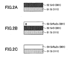
- a surface natural oxide film is removed by processing using 9% dilute hydrofluoric acid. Further, the thus processed single crystal silicon substrate 51 is introduced into the laser ablation apparatus 1 shown in FIG. 1 to act as the substrate 13, and a SrO film 52 having a rock salt structure was deposited on the single crystal silicon substrate 51 to a thickness of 5 to 6 nm by pulsed-laser deposition using a SrCO 3 target as the target 15 in FIG. 1.
- a SrRuO 3 film 53 was deposited on the SrO film 52 having a rock salt structure to a thickness of 100 nm by pulsed-laser deposition using a SrRuO 3 target as the target 15.
- the epitaxial SrO film 52 which is formed in the step shown in FIG. 2A on the surface of the silicon substrate of the (111) orientation, has the (001) orientation, and due to this, the epitaxial SrRuO 3 film 53, which is formed in the step shown in FIG. 2B on the epitaxial SrO film 52, also has the (001) orientation.
- FIG. 3 shows an X-ray diffraction pattern of the thus formed SrRuO 3 film 54.
- FIG. 4A illustrates an arrangement of silicon atoms in the (111) plane of silicon
- FIG. 4B illustrates epitaxial growth of a SrRuO 3 crystal on the (111) plane of silicon shown in FIG. 4A.
- the SrRuO 3 film 54 can be epitaxially grown on the (111) plane of the silicon crystal with the lattice thereof being matched with one of the three sides defining the (111) plane of the silicon crystal.
- the SrRuO 3 crystal has a pseudo-cubic axis in the direction of the c-axis, namely, the (001) direction, the (011) plane shown in FIG. 4 exists in four equivalent directions, as illustrated by arrows in FIG. 4C. Therefore, taking into consideration the (111) plane of silicon equivalently existing in three directions, in the SrRuO 3 epitaxial film 54, the c-axis is always aligned to be in the (001) direction, but the direction of the a-axis and the direction of the b-axis are different from each other, and hence there are totally 12 domains having different orientations. These domains constitute a twin crystal in the SrRuO 3 epitaxial film 54.
- FIG. 3 shows an X-ray diffraction pattern related to the (111) plane of the silicon crystal in the silicon substrate 51, which is measured with the silicon substrate 51 being rotated inside the plane of the substrate, that is, around an axis ( ⁇ axis) perpendicular to the substrate 51, and an X-ray diffraction pattern related to the (011) plane of the SrRuO 3 crystal in the SrRuO 3 film 54 formed on the silicon substrate 51, which is measured with the silicon substrate 51 being rotated inside the plane of the substrate.
- a capacitance device 50 shown in FIG. 6 is obtainable.
- the target 15 is changed to a SrTiO 3 target, and the laser beam 11 is irradiated at a pressure of 10 mTorr for 10 minutes with oxygen gas being supplied at a flow rate of 6 SCCM.
- the desired SrTiO 3 film 56 is obtained by epitaxial growth to have the (001) orientation.
- the substrate 51 is heated at a temperature of 600° C for one hour with oxygen gas being supplied at a flow rate of 5 liter per minute so as to recover damages in the SrTiO 3 film 56 induced in the course of sputtering of the Pt electrode 55.
- the SrRuO 3 film 54 is a single phase film with the SrO film 52 formed at the beginning, shown in FIG. 2A, being incorporated into by the mechanisms illustrated in FIG. 2B.
- the SrO film 52 remains between the silicon substrate 51 and the SrRuO 3 film 54 even after the step in FIG. 2C as illustrated in FIG. 7.
- FIG. 7 shows a capacitance device 50A as a modification to the capacitance device 50 in FIG. 6.
- FIG. 8A through FIG. 8D illustrate a process of forming an epitaxial SrRuO 3 film on the silicon (111) plane according to a second embodiment of the present invention.
- the same reference numbers are used for the same elements as described previously, and overlapping descriptions are omitted.
- FIG. 8A through FIG. 8D the steps in FIG. 8A through FIG. 8C are the same as those in FIG. 2A through FIG. 2C, that is, an epitaxial SrRuO 3 film 54 is formed in the step in FIG. 8C, corresponding to the step in FIG. 2C, on the silicon substrate 51 having a (111) orientation.
- the structure in FIG. 8C is heated at a temperature of 1050° C for two hours with vapor and oxygen carrier gas being supplied at a flow rate of 5 SLM, to form a thermal oxide film 51A in an interface of the SrRuO 3 film 54 and the silicon substrate 51, for example until the total thickness of the SrRuO 3 film 54 and the thermal oxide film 51A becomes 150 nm.
- FIG. 9 illustrates a configuration of a capacitance device 60 according to a third embodiment of the present invention.
- the same reference numbers are used for the same elements as described previously, and overlapping descriptions are omitted.
- An intermediate film 52A of good insulting property is interposed between the SrO film 52 and the SrRuO 3 epitaxial film 54.
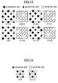
- the intermediate film 52A may be formed from compounds having a fluorite (CaF) structure as illustrated in FIG. 10, such as ZrO 2 , HfO 2 , CeO 2 , or PrO 2 , or oxides represented by the formula R 2 O 3 and having a C-rare-earth structure as illustrated in FIG. 11 (R represents Sc, Ce, Y, Pr, Nd, Eu, Tb, Dy, Ho, Yb, Y, Sm, Gd, Er, or La), or oxides represented by the formula R 2 O 3 and having an A-rare-earth structure (R represents La, Ce, Pr, Nd, or Gd), or compounds having a pyrochlore structure as illustrated in FIG. 12 and represented by the formula R 3 B'O 7 (where, R represents a trivalent rare-earth element, and B' represents a pentavalent transition-metal element).
- FIG. 13 shows a well-known rock salt structure.
- FIG. 10 through FIG. 13 are cross-sectional views illustrating atomic arrangements of positive ions and negative ions in a crystal in cross sectional planes cut at different heights Z along the direction of the c-axis, where Z represents a normalized height in a unit cell.
- the film 52 of a rock salt structure may be formed from a film having a main composition of MgO, CaO, BaO, SrO, or a mixture of them.
- the SrO film 52 in the structure shown in FIG. 9 is formed to be thin, after the SrRuO 3 epitaxial film 54 is formed, a structure can be formed in which the intermediate film 52A apparently is in contact with the silicon substrate 51.
- the FeRAM 100 is formed on a single crystal silicon substrate 101 having a (111) orientation, and includes a gate insulating film comprising a SrTiO 3 film 102 epitaxially formed on the single crystal silicon substrate 101, and a PZT film 103 epitaxially formed on the SrTiO 3 film 102.
- the SrTiO 3 film 102 is formed following the same steps as illustrated in FIG. 2A through FIG. 2C, except that a SrTiO 3 target is used as the target 15 instead of the SrRuO 3 target, and has a (001) orientation relative to the single crystal silicon substrate 101 of a (111) orientation, that is, with its c-axis being perpendicular to the primary surface of the substrate.
- the PZT film 103 formed on the SrTiO 3 film 102 also has the (001) orientation.
- the PZT film 103 can be formed, after the SrTiO 3 film 102 is formed and the target 15 is changed from SrTiO 3 to PZT, by irradiating a pulsed-laser beam 11 from a KrF excimer laser for 15 minutes at a substrate temperature of 650° C and a pressure of 200 mTorr with oxygen gas being supplied at a flow rate of 6 SCCM.
- the thus formed PZT film 103 is heated at a substrate temperature of 600° C for one hour with oxygen gas being supplied at a flow rate of 5 liter per minute so as to recover damages induced in the course of sputtering of the gate electrode 104.
- a thermal oxide film may be formed in an interface of the SrTiO 3 epitaxial film 102 and the silicon substrate 101 after growing the SrTiO 3 epitaxial film so as to reduce a gate leakage current.
- FIG. 6, FIG. 7, FIG. 9, or FIG. 14 may be employed.
- the SrTiO 3 epitaxial film 102 may also be omitted, and the PZT film 103 may be formed following the steps in FIG. 2A through FIG. 2C or in FIG. 8A through FIG. 8D.
- FIG. 16A and FIG. 16B illustrate a configuration of a SAW filter 200 according to a fifth embodiment of the present invention.
- the SAW filter 200 is formed on a single crystal silicon substrate 211 having a (111) orientation, and includes a SrTiO 3 epitaxial film 213 having a (001) orientation and formed on the single crystal silicon substrate 211 following the steps in FIG. 2A through FIG. 2C, and a PZT epitaxial film 213 having a (001) orientation and formed on the SrTiO 3 epitaxial film 213.
- an interdigital electrode 215 is formed on the PZT epitaxial film 214.
- ferroelectric PZT film 214 is a (001) alignment film, it can effectively excite elastic surface wave, and minimize loss.
- the silicon substrate After cleaning of a single crystal silicon substrate which has a diameter of two inches and has a (111) orientation, the silicon substrate is immersed into a 9% dilute hydrofluoric acid solution to remove a surface natural oxide film on the surface of the substrate.
- the thus processed single crystal silicon substrate is introduced into the laser ablation apparatus 1 shown in FIG. 1 to act as the substrate 13, and is maintained to be at a temperature of 800° C.
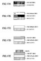
- the pressure inside the processing vessel 10 is lowered to be 5 x 10 -6 Torr, and then, a pulsed-laser beam 11 from a Nd: YAG laser is irradiated on a SrO target 15 for 1 minutes at a pressure of 5 x 10 -4 Torr with oxygen gas being supplied at a flow rate of 12 SCCM to execute the step in FIG. 17A, which corresponds to the step in FIG. 2A described previously.
- a SrO film 152 having the (001) orientation is epitaxially grown on the silicon substrate 151 having the (111) orientation, which corresponds to the substrate 13.
- the target 15 is changed to a SrRuO 3 target, and the laser beam 11 is irradiated to the SrRuO 3 target at a pressure of 100 mTorr for 10 minutes with oxygen gas being supplied at a flow rate of 6 SCCM.
- the SrRuO 3 film 153 is epitaxially grown on the SrO film 152 with the (001) orientation, whereas, Sr in the SrO film 152 diffuses into the SrRuO 3 film 153 deposited thereon, consequently, as illustrated in FIG. 17C, on the single crystal silicon substrate 151, the SrRuO 3 single phase film 153 is obtained with an epitaxial relation being maintained.
- the structure illustrated in FIG. 17C is taken out of the processing vessel 10, and is cooled. Then, 0.3 cc PLZT sol-gel solution with a composition ratio of Pb : La : Zr : Ti equaling 113 : 3 : 45 : 55 is dropped onto the SrRuO 3 film 154, and the substrate 151 is rotated, and then the solvent is vaporized on a hot plate maintained at a temperature of 350° C. Thereby, a PLZT spin-coat film 155 is formed on the SrRuO 3 film 154.
- thermal treatment is executed at a temperature of 650° C for 10 minutes with oxygen gas being supplied at a flow rate of 5 liter per minute so as to crystallize the PLZT spin-coat film 155.
- oxygen gas being supplied at a flow rate of 5 liter per minute so as to crystallize the PLZT spin-coat film 155.
- epitaxy between the PLZT spin-coat film 155 and the SrRuO 3 film 154 therebelow is being maintained, and the PLZT spin-coat film 155 is crystallized to have the (001) orientation.
- a Pt film is formed on the PLZT film 155 by sputtering with a predetermined mask, thereby forming a Pt electrode 156.
- the structure in FIG. 17E constitutes a unimorph piezoelectric actuator.
- the present invention by forming a metal oxide film having a rock salt structure on a single substrate having a (111) orientation, it is possible to control the metal oxide film to have a (001) orientation.
- the functional metal oxide film having a perovskite structure on the metal oxide film having the (001) orientation, it is possible to control the functional metal oxide film to have the (001) orientation which allows the properties of the functional metal oxide film to be exhibited strongly.
- By utilizing such a functional metal oxide film having the (001) orientation it is possible to fabricate devices having various functions, such as a ferroelectric random access memory, a SAW filter, or a ferroelectric actuator.
Landscapes
- Chemical & Material Sciences (AREA)
- Engineering & Computer Science (AREA)
- Crystallography & Structural Chemistry (AREA)
- Materials Engineering (AREA)
- Metallurgy (AREA)
- Organic Chemistry (AREA)
- Inorganic Chemistry (AREA)
- Physics & Mathematics (AREA)
- Acoustics & Sound (AREA)
- Manufacturing & Machinery (AREA)
- Semiconductor Memories (AREA)
- Non-Volatile Memory (AREA)
- Semiconductor Integrated Circuits (AREA)
- Formation Of Insulating Films (AREA)
- Crystals, And After-Treatments Of Crystals (AREA)
Applications Claiming Priority (1)
| Application Number | Priority Date | Filing Date | Title |
|---|---|---|---|
| PCT/JP2003/002516 WO2004079059A1 (ja) | 2003-03-04 | 2003-03-04 | (001)配向したペロブスカイト膜の形成方法、およびかかるペロブスカイト膜を有する装置 |
Publications (3)
| Publication Number | Publication Date |
|---|---|
| EP1600530A1 true EP1600530A1 (de) | 2005-11-30 |
| EP1600530A4 EP1600530A4 (de) | 2008-03-19 |
| EP1600530B1 EP1600530B1 (de) | 2011-05-11 |
Family
ID=32948245
Family Applications (1)
| Application Number | Title | Priority Date | Filing Date |
|---|---|---|---|
| EP20030816159 Expired - Lifetime EP1600530B1 (de) | 2003-03-04 | 2003-03-04 | Verfahren zur herstellung eines (001)-orientierten perowskitfilms und vorrichtung mit perowskitfilm |
Country Status (4)
| Country | Link |
|---|---|
| US (1) | US7339219B2 (de) |
| EP (1) | EP1600530B1 (de) |
| JP (1) | JP4401300B2 (de) |
| WO (1) | WO2004079059A1 (de) |
Cited By (1)
| Publication number | Priority date | Publication date | Assignee | Title |
|---|---|---|---|---|
| CN101107776B (zh) * | 2005-06-16 | 2010-05-19 | 株式会社村田制作所 | 压电器件及其制作方法 |
Families Citing this family (15)
| Publication number | Priority date | Publication date | Assignee | Title |
|---|---|---|---|---|
| US7247503B2 (en) * | 2003-05-07 | 2007-07-24 | Macronix International Co., Ltd. | Method of laser annealing to form an epitaxial growth layer |
| JP5240807B2 (ja) * | 2004-09-24 | 2013-07-17 | 独立行政法人産業技術総合研究所 | 光電変換構造体及びその製造方法 |
| KR100610150B1 (ko) | 2004-11-02 | 2006-08-09 | 재단법인서울대학교산학협력재단 | 질산 란타늄 완충층을 이용한 배향성 피제트티 박막 및 그증착공정 |
| JP4348547B2 (ja) * | 2005-04-14 | 2009-10-21 | セイコーエプソン株式会社 | ペロブスカイト型酸化物層の製造方法、強誘電体メモリの製造方法および表面波弾性波素子の製造方法 |
| WO2007094244A1 (ja) * | 2006-02-13 | 2007-08-23 | National Institute For Materials Science | ナノ超薄膜誘電体とその製造方法及びナノ超薄膜誘電体素子 |
| KR101405078B1 (ko) * | 2006-12-25 | 2014-06-10 | 도쿠리츠교세이호징 붓시쯔 자이료 겐큐키코 | 유전체 소자와 그 제조 방법 |
| JP4429346B2 (ja) | 2007-08-31 | 2010-03-10 | 富士通株式会社 | 半導体装置及びその製造方法 |
| US8866367B2 (en) | 2011-10-17 | 2014-10-21 | The United States Of America As Represented By The Secretary Of The Army | Thermally oxidized seed layers for the production of {001} textured electrodes and PZT devices and method of making |
| US9761785B2 (en) | 2011-10-17 | 2017-09-12 | The United States Of America As Represented By The Secretary Of The Army | Stylo-epitaxial piezoelectric and ferroelectric devices and method of manufacturing |
| KR20190008050A (ko) * | 2017-07-14 | 2019-01-23 | 에스케이하이닉스 주식회사 | 강유전성 메모리 소자 |
| WO2019116103A2 (en) * | 2017-12-12 | 2019-06-20 | Quantum Designed Materials Ltd. | Superconducting compounds and methods for making the same |
| FR3079531B1 (fr) * | 2018-03-28 | 2022-03-18 | Soitec Silicon On Insulator | Procede de fabrication d'une couche monocristalline de materiau pzt et substrat pour croissance par epitaxie d'une couche monocristalline de materiau pzt |
| US12052922B2 (en) * | 2020-03-26 | 2024-07-30 | Tdk Corporation | Piezoelectric thin film, piezoelectric thin film element and piezoelectric transducer |
| US11710775B2 (en) | 2020-05-29 | 2023-07-25 | Taiwan Semiconductor Manufacturing Co., Ltd. | Ferroelectric field effect transistor |
| KR102707431B1 (ko) * | 2021-06-23 | 2024-09-20 | 포항공과대학교 산학협력단 | 기판 상에 배치되는 이종의 단결정 전이 금속 산화물 층을 포함하는 전자 소자 및 이의 제조 방법 |
Family Cites Families (13)
| Publication number | Priority date | Publication date | Assignee | Title |
|---|---|---|---|---|
| US5650362A (en) * | 1993-11-04 | 1997-07-22 | Fuji Xerox Co. | Oriented conductive film and process for preparing the same |
| JP3199091B2 (ja) * | 1993-11-04 | 2001-08-13 | 富士ゼロックス株式会社 | 配向性薄膜の積層体 |
| JP3286181B2 (ja) * | 1995-11-17 | 2002-05-27 | ティーディーケイ株式会社 | 記録媒体およびその製造方法ならびに情報処理装置 |
| US5985404A (en) * | 1996-08-28 | 1999-11-16 | Tdk Corporation | Recording medium, method of making, and information processing apparatus |
| JP3684709B2 (ja) | 1996-10-03 | 2005-08-17 | 日産自動車株式会社 | 結晶性酸化物誘電体薄膜と単結晶シリコン基体との複合構造体およびそれを用いた電子素子およびそれらの製造方法 |
| JPH10120494A (ja) | 1996-10-22 | 1998-05-12 | Fuji Xerox Co Ltd | 強誘電体薄膜の製造方法 |
| JP3472087B2 (ja) * | 1997-06-30 | 2003-12-02 | Tdk株式会社 | 膜構造体、電子デバイス、記録媒体および酸化物導電性薄膜の製造方法 |
| JPH11133199A (ja) * | 1997-11-04 | 1999-05-21 | Hitachi Ltd | 固体ターゲット及び固体ターゲットシステム |
| JP3705695B2 (ja) * | 1998-03-12 | 2005-10-12 | 太陽誘電株式会社 | 層状ペロブスカイト構造の誘電体薄膜の作製方法、層状ペロブスカイト構造の誘電体薄膜及び層状ペロブスカイト構造の誘電体薄膜を有する電子部品 |
| US6278138B1 (en) * | 1998-08-28 | 2001-08-21 | Sony Corporation | Silicon-based functional matrix substrate and optical integrated oxide device |
| JP2001122698A (ja) * | 1999-10-26 | 2001-05-08 | Seiko Epson Corp | 酸化物電極薄膜 |
| JP4058971B2 (ja) * | 2001-03-26 | 2008-03-12 | セイコーエプソン株式会社 | 強誘電体メモリ及び電子機器 |
| JP2004006722A (ja) * | 2002-03-27 | 2004-01-08 | Seiko Epson Corp | 圧電アクチュエータ、インクジェット式ヘッド及び吐出装置 |
-
2003
- 2003-03-04 EP EP20030816159 patent/EP1600530B1/de not_active Expired - Lifetime
- 2003-03-04 JP JP2004569083A patent/JP4401300B2/ja not_active Expired - Fee Related
- 2003-03-04 WO PCT/JP2003/002516 patent/WO2004079059A1/ja not_active Ceased
-
2005
- 2005-02-24 US US11/063,731 patent/US7339219B2/en not_active Expired - Fee Related
Cited By (1)
| Publication number | Priority date | Publication date | Assignee | Title |
|---|---|---|---|---|
| CN101107776B (zh) * | 2005-06-16 | 2010-05-19 | 株式会社村田制作所 | 压电器件及其制作方法 |
Also Published As
| Publication number | Publication date |
|---|---|
| US7339219B2 (en) | 2008-03-04 |
| EP1600530A4 (de) | 2008-03-19 |
| JPWO2004079059A1 (ja) | 2006-06-08 |
| WO2004079059A1 (ja) | 2004-09-16 |
| EP1600530B1 (de) | 2011-05-11 |
| US20050213282A1 (en) | 2005-09-29 |
| JP4401300B2 (ja) | 2010-01-20 |
Similar Documents
| Publication | Publication Date | Title |
|---|---|---|
| US5955213A (en) | Ferroelectric thin film, electric device, and method for preparing ferroelectric thin film | |
| JP3193302B2 (ja) | 膜構造体、電子デバイス、記録媒体および強誘電体薄膜の製造方法 | |
| US6096434A (en) | Film structure, electronic device, recording medium, and method for forming conductive oxide thin films | |
| JP3310881B2 (ja) | 積層薄膜、電子デバイス用基板、電子デバイスおよび積層薄膜の製造方法 | |
| US5753934A (en) | Multilayer thin film, substrate for electronic device, electronic device, and preparation of multilayer oxide thin film | |
| JP4734823B2 (ja) | 膜多層構造体及びこれを用いるアクチュエータ素子、容量素子、フィルタ素子 | |
| EP1600530B1 (de) | Verfahren zur herstellung eines (001)-orientierten perowskitfilms und vorrichtung mit perowskitfilm | |
| JP3999300B2 (ja) | 強誘電体薄膜およびその製造方法 | |
| US20070190363A1 (en) | Heterolayered ferroelectric thin films and methods of forming same | |
| US6747317B2 (en) | Semiconductor device | |
| JP4483849B2 (ja) | 強誘電体薄膜 | |
| JP3669860B2 (ja) | 積層薄膜 | |
| JP4142128B2 (ja) | 積層薄膜およびその製造方法 | |
| KR100795664B1 (ko) | (001) 배향된 페로브스카이트막의 형성 방법, 및 이러한페로브스카이트막을 갖는 장치 | |
| JP4142127B2 (ja) | 積層薄膜およびその製造方法 | |
| JP2002521820A (ja) | 層状超格子材料の製造および層状超格子材料を含む電子デバイスを作製するための低温プロセス | |
| JPH0955544A (ja) | 電子デバイス用基板 | |
| JPH11231153A (ja) | 強誘電体薄膜素子の製造方法 |
Legal Events
| Date | Code | Title | Description |
|---|---|---|---|
| PUAI | Public reference made under article 153(3) epc to a published international application that has entered the european phase |
Free format text: ORIGINAL CODE: 0009012 |
|
| 17P | Request for examination filed |
Effective date: 20050223 |
|
| AK | Designated contracting states |
Kind code of ref document: A1 Designated state(s): AT BE BG CH CY CZ DE DK EE ES FI FR GB GR HU IE IT LI LU MC NL PT RO SE SI SK TR |
|
| RBV | Designated contracting states (corrected) |
Designated state(s): DE FR IT |
|
| A4 | Supplementary search report drawn up and despatched |
Effective date: 20080214 |
|
| 17Q | First examination report despatched |
Effective date: 20080527 |
|
| GRAP | Despatch of communication of intention to grant a patent |
Free format text: ORIGINAL CODE: EPIDOSNIGR1 |
|
| GRAS | Grant fee paid |
Free format text: ORIGINAL CODE: EPIDOSNIGR3 |
|
| GRAA | (expected) grant |
Free format text: ORIGINAL CODE: 0009210 |
|
| AK | Designated contracting states |
Kind code of ref document: B1 Designated state(s): DE FR IT |
|
| REG | Reference to a national code |
Ref country code: DE Ref legal event code: R096 Ref document number: 60337107 Country of ref document: DE Effective date: 20110622 |
|
| PLBE | No opposition filed within time limit |
Free format text: ORIGINAL CODE: 0009261 |
|
| STAA | Information on the status of an ep patent application or granted ep patent |
Free format text: STATUS: NO OPPOSITION FILED WITHIN TIME LIMIT |
|
| 26N | No opposition filed |
Effective date: 20120214 |
|
| REG | Reference to a national code |
Ref country code: DE Ref legal event code: R097 Ref document number: 60337107 Country of ref document: DE Effective date: 20120214 |
|
| REG | Reference to a national code |
Ref country code: FR Ref legal event code: PLFP Year of fee payment: 14 |
|
| REG | Reference to a national code |
Ref country code: FR Ref legal event code: PLFP Year of fee payment: 15 |
|
| PGFP | Annual fee paid to national office [announced via postgrant information from national office to epo] |
Ref country code: FR Payment date: 20170213 Year of fee payment: 15 Ref country code: DE Payment date: 20170228 Year of fee payment: 15 |
|
| PGFP | Annual fee paid to national office [announced via postgrant information from national office to epo] |
Ref country code: IT Payment date: 20170320 Year of fee payment: 15 |
|
| REG | Reference to a national code |
Ref country code: DE Ref legal event code: R119 Ref document number: 60337107 Country of ref document: DE |
|
| PG25 | Lapsed in a contracting state [announced via postgrant information from national office to epo] |
Ref country code: DE Free format text: LAPSE BECAUSE OF NON-PAYMENT OF DUE FEES Effective date: 20181002 |
|
| PG25 | Lapsed in a contracting state [announced via postgrant information from national office to epo] |
Ref country code: IT Free format text: LAPSE BECAUSE OF NON-PAYMENT OF DUE FEES Effective date: 20180304 |
|
| PG25 | Lapsed in a contracting state [announced via postgrant information from national office to epo] |
Ref country code: FR Free format text: LAPSE BECAUSE OF NON-PAYMENT OF DUE FEES Effective date: 20180331 |