EP1578118B1 - Halbleiterbildaufnahmevorrichtung und ihr Ansteuerverfahren - Google Patents
Halbleiterbildaufnahmevorrichtung und ihr Ansteuerverfahren Download PDFInfo
- Publication number
- EP1578118B1 EP1578118B1 EP04255170.5A EP04255170A EP1578118B1 EP 1578118 B1 EP1578118 B1 EP 1578118B1 EP 04255170 A EP04255170 A EP 04255170A EP 1578118 B1 EP1578118 B1 EP 1578118B1
- Authority
- EP
- European Patent Office
- Prior art keywords
- reset
- dummy
- row
- rows
- read
- Prior art date
- Legal status (The legal status is an assumption and is not a legal conclusion. Google has not performed a legal analysis and makes no representation as to the accuracy of the status listed.)
- Expired - Lifetime
Links
Images


Classifications
-
- H—ELECTRICITY
- H04—ELECTRIC COMMUNICATION TECHNIQUE
- H04N—PICTORIAL COMMUNICATION, e.g. TELEVISION
- H04N25/00—Circuitry of solid-state image sensors [SSIS]; Control thereof
- H04N25/50—Control of the SSIS exposure
- H04N25/53—Control of the integration time
- H04N25/531—Control of the integration time by controlling rolling shutters in CMOS SSIS
-
- H—ELECTRICITY
- H04—ELECTRIC COMMUNICATION TECHNIQUE
- H04N—PICTORIAL COMMUNICATION, e.g. TELEVISION
- H04N25/00—Circuitry of solid-state image sensors [SSIS]; Control thereof
- H04N25/60—Noise processing, e.g. detecting, correcting, reducing or removing noise
- H04N25/67—Noise processing, e.g. detecting, correcting, reducing or removing noise applied to fixed-pattern noise, e.g. non-uniformity of response
- H04N25/671—Noise processing, e.g. detecting, correcting, reducing or removing noise applied to fixed-pattern noise, e.g. non-uniformity of response for non-uniformity detection or correction
- H04N25/677—Noise processing, e.g. detecting, correcting, reducing or removing noise applied to fixed-pattern noise, e.g. non-uniformity of response for non-uniformity detection or correction for reducing the column or line fixed pattern noise
-
- H—ELECTRICITY
- H04—ELECTRIC COMMUNICATION TECHNIQUE
- H04N—PICTORIAL COMMUNICATION, e.g. TELEVISION
- H04N25/00—Circuitry of solid-state image sensors [SSIS]; Control thereof
- H04N25/70—SSIS architectures; Circuits associated therewith
- H04N25/76—Addressed sensors, e.g. MOS or CMOS sensors
Definitions
- the present invention relates to a solid state imaging device provided with an imaging element, such as a CMOS image sensor.
- An XY address-type solid state imaging device includes a plurality of imaging elements arranged in a matrix. An image of an object is acquired by scanning the imaging elements in a vertical direction. During this imaging operation, that is, during the operation of an electronic shutter, the electrical charge stored in each imaging element is reset in response to a reset signal. After the reset, the charge stored by each imaging element is read according to a read signal.
- band-like electronic shutter noise difference in brightness level or difference in contrast level
- the shutter noise extends along a horizontal direction in the image. In order to stably obtain high quality images, the generation of such electronic shutter noise must be suppressed.
- Fig. 1 shows the pixel array of an XY address-type solid state imaging device. Pixel regions 1 are arranged in a matrix. Each pixel region 1 is connected to a vertical selection line CL and a horizontal selection line SLCT. A photoelectric conversion element, such as a photodiode 2, is formed in each pixel region 1.
- an n-channel MOS transistor Tr1 is connected to a power supply VDD, which supplies reset voltage.
- the cathode of a photodiode 2 is connected to the n-channel MOS transistor Tr1. Accordingly, the reset voltage is supplied through the n-channel MOS transistor Tr1 to the cathode of the photodiode 2.
- a low potential power supply VSS is connected to the anode of the photodiode 2.
- a reset signal line RST is connected to the gate of the transistor Tr1.
- the source of the transistor Tr1 is connected to the gate of an n-channel MOS transistor Tr2.
- the drain of the transistor Tr2 is connected to the power supply VDD.
- the source of the transistor Tr2 is connected to the vertical selection line CL via an n-channel MOS transistor Tr3.
- the gate of the transistor Tr3 is connected to the horizontal selection line SLCT.
- the reset signal lines RST are sequentially selected by a reset control circuit.
- the transistor Tr1 of the pixel region 1 connected to the selected reset signal line RST is turned ON, a photodiode 2 is reset by the reset voltage level of the power supply VDD, and exposure of the photodiode 2 is started.
- the photodiode 2 is discharged in accordance with the amount of exposure.
- the horizontal selection lines SLCT are sequentially selected in accordance with the operation of a vertical scan shift register.
- the transistor Tr3 connected to the selected horizontal selection line SLCT is turned ON.
- the pixel data corresponding to the charge potential at the photodiode 2 is output to the associated vertical selection line CL.
- a column parallel reading circuit simultaneously reads pixel data, which is read from each pixel region 1 in one horizontal row of the pixel array, through all the vertical selection lines CL. Then, the pixel data is sequentially selected by the horizontal scan shift register and output from an output circuit.
- Fig. 2 shows the pixel array at a specific timing. At this time, row L1 is undergoing a reset process, and row L2 is undergoing a read process. The reset row L1 and the read row L2 are separated from each other by a predetermined row spacing L. At the next timing, the reset row L1 and the read row L2 are shifted downward by one row.
- the row spacing L corresponds to the time from when the reset operation is performed to when the read operation is performed, that is, the integration time (exposure time) of each photodiode 2.
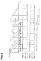
- Fig. 3 shows the timing of a rolling shutter operation when the interval between a reset operation AC1 and a read operation AC2 is equivalent to the time for scanning 100 rows (that is, the row spacing L is 100 rows).
- the total number of rows of the pixel regions 1 is 640, and the vertical blanking period is equivalent to the time for scanning 45 rows.
- the reset operation AC1 starts to sequentially select the reset signal lines RST.
- period t1 which is equivalent to the time for resetting 100 rows
- the read operation AC2 is started to sequentially select the horizontal selection lines SLCT.
- period t2 the reset operation AC1 of frame FL1 ends.
- period t3 the read operation AC2 of frame FL1 ends.
- the vertical blanking period t4 which is equivalent to the time for scanning 45 rows elapses, the imaging operation of the first frame FL1 ends, and the reset operation AC1 of the next frame starts.
- an imaging device has been proposed to level the load on the power supply VDD by providing a plurality of dummy rows in the pixel array. For example, as shown in Fig. 3 , a reset operation is performed on the dummy rows at periods t3 and t4 during which the reset operation AC1 is not performed. A read operation is performed for the dummy rows at periods t1 and t4 during which the read operation is not performed.
- Japanese Laid-Open Patent Publication No. 2001-8109 and Japanese Laid-Open Patent Publication No. 2000-125203 each describe an imaging device in which a reset operation is performed on dummy rows from when a reset operation ends to when a read operation ends.
- US 6,507,365 discloses a solid-state imaging device with a variable (continuous) electronic shutter function.
- the imaging device comprises an imaging area where unit cells with photodiodes acting as pixels are arranged two-dimensionally, read lines for driving the read transistors in each pixel row, vertical selection lines for driving the vertical selection transistors in each pixel row, a vertical driving circuit for selectively driving vertical selection lines, vertical signal lines for outputting the signal from each unit cell in the pixel rows driven sequentially, and a row selection circuit for controlling the vertical driving circuit in such a manner that the vertical driving circuit drives the read transistors in each pixel row with the desired signal storage timing and signal read timing twice in that order and thereby drives the vertical selection transistors in the pixel row in synchronization with the signal read timing.
- the integration time of each pixel region must be increased when the brightness of the imaged object decreases.
- the period between the reset operation AC1 and the read operation AC2 corresponds to 100 rows.
- the period between the reset operation AC1 and the read operation AC2 corresponds to 500 rows.
- the reset operation AC1 is performed 500 rows before the read operation AC2 when starting frame FL4. That is, at period t5, the reset operation AC1 of frame FL4 is performed in parallel with frame FL3. In other words, when the reset operation is performed for two rows at period t5, a read operation AC2 is performed in parallel for one row.
- the load of the power supply VDD fluctuates at period t5 and generates electronic shutter noise in the acquired image of frame FL3 or FL4.
- the present invention provides a method for driving a solid state imaging device which prevents electronic shutter noise from being produced even when the integration time for exposing pixel regions changes.
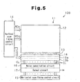
- a solid state imaging device 100 is provided with a pixel array unit 11 including a pixel array 12 and a three-row dummy array 13 adjacent to the pixel array 12.
- the pixel array 12 and the dummy array 13 include a plurality of pixel regions arrayed in a matrix pattern. Each pixel region is connected to a reset signal line RST, a horizontal selection line SLCT, and a vertical selection line CL.
- the configuration of each pixel region is identical to that shown in Fig. 1 .
- a vertical scan timing control circuit 14 controls the reset operation and read operation of the pixel array 12 and the dummy array 13.
- the reset signal lines RST are sequentially selected within the pixel array 12 in accordance with a reset signal RSn output from a reset control circuit in the vertical scan timing control circuit 14.
- the horizontal selection lines SLCT are sequentially selected within the pixel array 12 in accordance with a read signal RDn output from a vertical scan shift register in the vertical scan timing control circuit 14. Pixel data from the pixel region that is connected to the selected horizontal selection line SLCT is output to the associated vertical selection line CL.
- a horizontal scan timing control circuit 15 selects a vertical selection line CL.
- the pixel data of the selected vertical selection line CL is sequentially output from an output circuit 17 through a noise cancellation circuit 16.
- the dummy array 13 includes one dummy read row 18 and two dummy reset rows 19a and 19b. Further, the dummy array 13 is controlled by the vertical scan timing control circuit 14.
- the vertical scan timing control circuit 14 selects the dummy read row 18 in each frame during an imaging operation when the horizontal selection line SLCT selection operation is not being performed in the pixel array 12, that is, when the read operation is not being performed. However, the vertical scan timing control circuit 14 does not select the dummy read row 18 when the horizontal selection line SLCT selection operation is being performed.
- the vertical scan timing control circuit 14 selects the two dummy reset rows 19a and 19b when the reset signal line RST selection operation is not being performed in the pixel array 12, that is, when the reset operation is not being performed.
- the vertical scan timing control circuit 14 selects only the dummy reset row 19a when one reset signal line RST is selected.
- the vertical scan timing control circuit 14 does not select any of the dummy reset rows 19a and 19b when two reset signal line RST selection operations are performed in parallel.
- This operation is based on the logic of the selection signals of the reset signal line RST and the horizontal selection line SLCT.
- Fig. 4 shows the timing of an operation when the interval between a reset operation AC1 and a read operation AC2 is equivalent to the time for scanning 100 rows (that is, the row spacing L is 100 rows).
- the total number of rows of the pixel regions 1 is 640, and the vertical blanking period is equivalent to the time for scanning 45 rows.
- the reset operation AC1 for sequentially selecting the reset signal line RST starts.
- the read operation AC2 for sequentially selecting the horizontal selection line SLCT starts after period t1, which is equivalent to the time for resetting 100 rows.
- the reset operation AC1 of frame FL1 ends after period t2.
- the read operation AC2 of frame FL1 ends after period t3.
- the vertical blanking period t4 which is equivalent to the time for scanning 45 rows, elapses, the imaging operation of the first frame FL1 ends, and the reset operation AC1 of the next frame FL2 starts.
- the vertical scan timing control circuit 14 selects the dummy read row 18 and does not perform the selection operation on the horizontal selection lines SLCT. Furthermore, the vertical scan timing control circuit 14 performs the selection operation on the reset signal lines RST, selects one reset row, and selects the dummy reset row 19a. Accordingly, when one row is read, two reset rows are selected in parallel.
- the reset operation AC1 and the read operation AC2 are performed in parallel.
- the vertical scan timing control circuit 14 performs the selection operation on the horizontal selection lines SLCT but does not select the dummy read row 18. Furthermore, the vertical scan timing control circuit 14 performs the selection operation on the reset signal lines RST, selects one reset row, and selects the dummy reset row 19a. Accordingly, when one row is read, two reset rows are selected in parallel.
- the vertical scan timing control circuit 14 performs the selection operation on the horizontal selection lines SLCT but does not select the dummy read row 18. Furthermore, the vertical scan timing control circuit 14 selects the two dummy reset rows 19a and 19b but does not perform the selection operation on the reset signal lines RST. Accordingly, when one row is read, two reset rows are selected in parallel.
- the integration time (exposure time) of each pixel region increases when the brightness of the scanning object decreases during the imaging operation of the imaging device 100.
- the period between the reset operation AC1 and the read operation AC2 is changed to 500 rows.
- the reset operation AC1 is performed 500 rows before the read operation AC2, which has a fixed cycle.
- the reset operations AC1 of frames FL3 and FL4 are performed in parallel.
- the vertical scan timing control circuit 14 performs two selection operations on the reset signal lines RST and one selection operation on the horizontal selection line SLCT in parallel.
- the vertical scan timing control circuit 14 performs the selection operation on the horizontal selection lines SLCT but does not select the dummy read row 18.
- the vertical scan timing control circuit 14 performs two selection operations on the reset signal line RST but does not select the dummy reset row. Accordingly, when one row is read, two reset rows are selected in parallel.
- the imaging device 100 of the preferred embodiment has the advantages described below.
- a plurality of dummy read rows may be used. This would suppress load fluctuation when reading a plurality of rows.
- the present invention provides, in one aspect, a method for driving a solid state imaging device (100) which prevents the generation of electronic shutter noise even when the integration time for exposure of a pixel region fluctuates.
- the solid state imaging device (100) performs a rolling shutter operation that sequentially selects a reset row and a read row separated from each other in accordance with a row spacing based on integration time in the pixel array (12).
- a dummy row (18, 19a, 19b) is selected when a reset row or a read row is not selected.
- the method includes selecting none, one, or more than one dummy reset row (19a, 19b) so that the total of the number of the reset rows and the reset dummy rows that are simultaneously selected is constant regardless of the number of simultaneously selected reset rows.
Landscapes
- Engineering & Computer Science (AREA)
- Multimedia (AREA)
- Signal Processing (AREA)
- Transforming Light Signals Into Electric Signals (AREA)
- Solid State Image Pick-Up Elements (AREA)
Claims (4)
- Verfahren zum Ansteuern einer Bildaufnahmevorrichtung (100), welche in einem Rollblendenmodus zu betreiben ist, in welchem die Bildaufnahmevorrichtung (100) aus einer Pixelfeldeinheit (11) nacheinander eine Rückstellreihe und eine Lesereihe mit einem Reihenabstand auswählt, der einer Integrationszeit der Bildaufnahmevorrichtung (100) entspricht, und eine oder mehrere Rückstell-Blindreihen oder eine oder mehrere Lese-Blindreihen auswählt, wenn keine Rückstellreihe oder Lesereihe ausgewählt wird, wobei das Verfahren Folgendes umfasst:Auswählen von zwei Rückstell-Blindreihen, wenn keine Rückstellreihe ausgewählt wird, und Auswählen einer Rückstell-Blindreihen, wenn eine Rückstellreihe ausgewählt wird, so dass die Summe aus der Anzahl aktuell ausgewählter Lesereihen, der Anzahl aktuell ausgewählter Lese-Blindreihen, der Anzahl aktuell ausgewählter Rückstellreihen und der Anzahl aktuell ausgewählter Rückstell-Blindreihen konstant ist, ungeachtet der Anzahl gleichzeitig ausgewählter Lesereihen und Rückstellreihen; undwenn die Integrationszeit erhöht wird, Auswählen von keiner Rückstell-Blindreihe, wenn zwei Rückstellreihen mit einem Reihenabstand in Abhängigkeit von der Erhöhung der Integrationszeit ausgewählt werden; dadurch gekennzeichnet, dass:die Summe konstant ist, auch wenn die Bildaufnahmeoperation eines Anfangsrahmens beginnt.
- Bildaufnahmevorrichtung (100), umfassend eine Pixelfeldeinheit (11), welche ein Pixelfeld (12) umfasst;
ein Blindfeld (13), welches mindestens eine Rückstell-Blindreihe und mindestens eine Lese-Blindreihe umfasst; und
eine Vertikalabtastungs-Zeitregelungs-Schaltung (14), welche dafür eingerichtet ist, einen Rollblendenmodus durchzuführen, bei welchem die Vertikalabtastungs-Zeitregelungs-Schaltung (14) aus der Pixelfeldeinheit (11) nacheinander eine Rückstellreihe und eine Lesereihe mit einem Abstand auswählt, der einer Integrationszeit der Bildaufnahmevorrichtung (100) entspricht, und eine oder mehrere Rückstell-Blindreihen oder eine oder mehrere Lese-Blindreihen auswählt, wenn keine Rückstellreihe und keine Lesereihe ausgewählt wird, wobei die Vertikalabtastungs-Zeitregelungs-Schaltung (14) für Folgendes eingerichtet ist:Auswählen einer Anzahl von Rückstell-Blindreihen, die so eingestellt sind, dass die Summe aus der Anzahl aktuell ausgewählter Lesereihen, der Anzahl aktuell ausgewählter Lese-Blindreihen, der Anzahl aktuell ausgewählter Rückstellreihen und der Anzahl aktuell ausgewählter Rückstell-Blindreihen konstant ist, ungeachtet der Anzahl gleichzeitig ausgewählter Lesereihen und Rückstellreihen;Auswählen von zwei Rückstell-Blindreihen, wenn keine Rückstellreihe ausgewählt wird;Auswählen einer Rückstell-Blindreihen, wenn eine Rückstellreihe ausgewählt wird; undwenn die Integrationszeit erhöht wird, Auswählen von keiner Rückstell-Blindreihe, wenn zwei Rückstellreihen mit einem Reihenabstand in Abhängigkeit von der Erhöhung der Integrationszeit ausgewählt werden; dadurch gekennzeichnet, dass:die Summe konstant ist, auch wenn die Bildaufnahmeoperation eines Anfangsrahmens beginnt. - Bildaufnahmevorrichtung nach Anspruch 2, dadurch gekennzeichnet, dass die Vertikalabtastungs-Zeitregelungs-Schaltung (14) ferner für Folgendes eingerichtet ist:Auswählen einer Lese-Blindreihe, wenn keine Lesereihe ausgewählt wird; undAuswählen einer Lesereihe, wenn keine Lese-Blindreihe ausgewählt wird.
- Bildaufnahmevorrichtung nach Anspruch 2 oder 3, wobei das Blindfeld eine Lese-Blindreihe und zwei Rückstell-Blindreihen umfasst und die Vertikalabtastungs-Zeitregelungs-Schaltung (14) dafür eingerichtet ist, laufend dieselbe Lese-Blindreihe oder dieselbe Rückstell-Blindreihe auszuwählen, wenn die Lese-Blindreihe und die Rückstell-Blindreihe ausgewählt werden, so dass eine Lese- oder Rückstell-Blindoperation immer unter identischen Bedingungen durchgeführt wird.
Applications Claiming Priority (2)
| Application Number | Priority Date | Filing Date | Title |
|---|---|---|---|
| JP2004076909A JP4354854B2 (ja) | 2004-03-17 | 2004-03-17 | 固体撮像装置の駆動方法及び固体撮像装置 |
| JP2004076909 | 2004-03-17 |
Publications (3)
| Publication Number | Publication Date |
|---|---|
| EP1578118A2 EP1578118A2 (de) | 2005-09-21 |
| EP1578118A3 EP1578118A3 (de) | 2008-07-16 |
| EP1578118B1 true EP1578118B1 (de) | 2015-01-28 |
Family
ID=34836554
Family Applications (1)
| Application Number | Title | Priority Date | Filing Date |
|---|---|---|---|
| EP04255170.5A Expired - Lifetime EP1578118B1 (de) | 2004-03-17 | 2004-08-26 | Halbleiterbildaufnahmevorrichtung und ihr Ansteuerverfahren |
Country Status (6)
| Country | Link |
|---|---|
| US (1) | US7489353B2 (de) |
| EP (1) | EP1578118B1 (de) |
| JP (1) | JP4354854B2 (de) |
| KR (1) | KR100634860B1 (de) |
| CN (1) | CN1671188B (de) |
| TW (1) | TWI257249B (de) |
Families Citing this family (24)
| Publication number | Priority date | Publication date | Assignee | Title |
|---|---|---|---|---|
| US7214945B2 (en) * | 2002-06-11 | 2007-05-08 | Canon Kabushiki Kaisha | Radiation detecting apparatus, manufacturing method therefor, and radiation image pickup system |
| US7841533B2 (en) | 2003-11-13 | 2010-11-30 | Metrologic Instruments, Inc. | Method of capturing and processing digital images of an object within the field of view (FOV) of a hand-supportable digitial image capture and processing system |
| JP4025836B2 (ja) * | 2004-10-07 | 2007-12-26 | コニカミノルタオプト株式会社 | 撮像装置及び携帯通信機器 |
| JP4687155B2 (ja) * | 2005-03-09 | 2011-05-25 | ソニー株式会社 | 固体撮像装置およびその駆動方法 |
| JP4756960B2 (ja) * | 2005-09-02 | 2011-08-24 | キヤノン株式会社 | 撮像装置及びその制御方法、コンピュータプログラム及び記憶媒体 |
| WO2007065964A1 (en) * | 2005-12-07 | 2007-06-14 | Nokia Corporation | Camera unit and method for controlling an image sensor in a camera unit |
| US8059174B2 (en) * | 2006-05-31 | 2011-11-15 | Ess Technology, Inc. | CMOS imager system with interleaved readout for providing an image with increased dynamic range |
| JP4887935B2 (ja) * | 2006-06-28 | 2012-02-29 | パナソニック株式会社 | 撮像装置および露光時間制御方法 |
| JP5163935B2 (ja) * | 2007-05-17 | 2013-03-13 | ソニー株式会社 | イメージセンサ |
| JP4442669B2 (ja) * | 2007-09-18 | 2010-03-31 | ソニー株式会社 | 固体撮像素子およびカメラシステム |
| US7866557B2 (en) * | 2007-09-27 | 2011-01-11 | Symbol Technologies, Inc. | Imaging-based bar code reader utilizing modified rolling shutter operation |
| JP5282543B2 (ja) * | 2008-11-28 | 2013-09-04 | ソニー株式会社 | 固体撮像装置、固体撮像装置の駆動方法および撮像装置 |
| JP5263023B2 (ja) * | 2009-06-17 | 2013-08-14 | ペンタックスリコーイメージング株式会社 | 撮像装置 |
| CN101989606B (zh) * | 2009-07-29 | 2013-04-03 | 英属开曼群岛商恒景科技股份有限公司 | 具外围假像素的影像传感器 |
| US8605177B2 (en) * | 2009-09-16 | 2013-12-10 | Altasens, Inc. | Image sensor with wide dynamic range |
| JP5434485B2 (ja) | 2009-11-02 | 2014-03-05 | ソニー株式会社 | 固体撮像素子、固体撮像素子の駆動方法、およびカメラシステム |
| JP5403369B2 (ja) * | 2010-03-31 | 2014-01-29 | ソニー株式会社 | 固体撮像素子および駆動方法、並びに電子機器 |
| TW201216138A (en) * | 2010-10-13 | 2012-04-16 | Chunghwa Picture Tubes Ltd | Method for driving photosensor array panel |
| JP5447430B2 (ja) * | 2011-04-27 | 2014-03-19 | 株式会社ニコン | 撮像装置 |
| US8975570B2 (en) | 2012-08-23 | 2015-03-10 | Teledyne Dalsa Inc. | CMOS time delay and integration image sensor |
| US9148601B2 (en) * | 2012-09-26 | 2015-09-29 | Teledyne Dalsa, Inc. | CMOS TDI image sensor with rolling shutter pixels |
| FR3000347B1 (fr) * | 2012-12-21 | 2016-03-04 | Trixell | Procede de lecture d'un dispositif d'imagerie |
| JP5652532B2 (ja) * | 2013-10-31 | 2015-01-14 | ソニー株式会社 | 固体撮像素子および駆動方法、並びに電子機器 |
| KR102747643B1 (ko) * | 2019-07-25 | 2024-12-27 | 삼성전자주식회사 | 이미지 센서 및 이의 동작 방법 |
Family Cites Families (11)
| Publication number | Priority date | Publication date | Assignee | Title |
|---|---|---|---|---|
| US5083016A (en) * | 1990-03-27 | 1992-01-21 | Hughes Aircraft Company | 3-transistor source follower-per-detector unit cell for 2-dimensional focal plane arrays |
| JPH11164210A (ja) | 1997-11-28 | 1999-06-18 | Nikon Corp | 動き検出用固体撮像装置 |
| US6529242B1 (en) * | 1998-03-11 | 2003-03-04 | Micron Technology, Inc. | Look ahead shutter pointer allowing real time exposure control |
| US6847398B1 (en) * | 1998-03-31 | 2005-01-25 | Micron Technology, Inc. | Latched row logic for a rolling exposure snap |
| KR100352757B1 (ko) * | 1998-06-02 | 2002-09-16 | 가부시끼가이샤 도시바 | 고속도 동작 고체 촬상 장치 |
| JP3512152B2 (ja) * | 1998-10-14 | 2004-03-29 | 松下電器産業株式会社 | 増幅型固体撮像装置およびその駆動方法 |
| JP4087971B2 (ja) * | 1999-01-29 | 2008-05-21 | 東芝デジタルメディアエンジニアリング株式会社 | 固体撮像装置 |
| TW439285B (en) * | 1998-11-30 | 2001-06-07 | Toshiba Corp | Solid-state imaging device |
| JP2001008109A (ja) | 1999-06-23 | 2001-01-12 | Sony Corp | 固体撮像素子およびその駆動方法並びにカメラシステム |
| JP3875461B2 (ja) | 2000-07-06 | 2007-01-31 | 株式会社東芝 | 固体撮像システム |
| JP4117540B2 (ja) * | 2002-10-17 | 2008-07-16 | ソニー株式会社 | 固体撮像素子の制御方法 |
-
2004
- 2004-03-17 JP JP2004076909A patent/JP4354854B2/ja not_active Expired - Fee Related
- 2004-08-26 US US10/925,919 patent/US7489353B2/en not_active Expired - Fee Related
- 2004-08-26 EP EP04255170.5A patent/EP1578118B1/de not_active Expired - Lifetime
- 2004-08-30 TW TW093126027A patent/TWI257249B/zh not_active IP Right Cessation
- 2004-09-17 CN CN2004100782151A patent/CN1671188B/zh not_active Expired - Fee Related
- 2004-09-17 KR KR1020040074389A patent/KR100634860B1/ko not_active Expired - Fee Related
Also Published As
| Publication number | Publication date |
|---|---|
| US7489353B2 (en) | 2009-02-10 |
| EP1578118A2 (de) | 2005-09-21 |
| EP1578118A3 (de) | 2008-07-16 |
| US20050206762A1 (en) | 2005-09-22 |
| KR20050093677A (ko) | 2005-09-23 |
| TW200533190A (en) | 2005-10-01 |
| CN1671188A (zh) | 2005-09-21 |
| TWI257249B (en) | 2006-06-21 |
| KR100634860B1 (ko) | 2006-10-17 |
| JP4354854B2 (ja) | 2009-10-28 |
| JP2005269098A (ja) | 2005-09-29 |
| CN1671188B (zh) | 2012-02-22 |
Similar Documents
| Publication | Publication Date | Title |
|---|---|---|
| EP1578118B1 (de) | Halbleiterbildaufnahmevorrichtung und ihr Ansteuerverfahren | |
| US7656449B2 (en) | Solid-state imaging apparatus having gate potential that is negtive with respect to a well region | |
| KR101424033B1 (ko) | 고체 촬상 장치, 고체 촬상 장치의 구동 방법 및 촬상 장치 | |
| US8159577B2 (en) | Solid-state imaging apparatus with decoders for controlling reset switches | |
| US7499091B2 (en) | Solid-state imaging device and method for driving same | |
| JP5556199B2 (ja) | 固体撮像素子及び撮像機器 | |
| US20140125855A1 (en) | Method of acquiring physical information and physical information acquiring device | |
| JP4403387B2 (ja) | 固体撮像装置および固体撮像装置の駆動方法 | |
| JP2002209144A (ja) | 画像センサ | |
| JP2000125203A (ja) | 増幅型固体撮像装置およびその駆動方法 | |
| US7619674B2 (en) | CMOS image sensor with wide dynamic range | |
| KR20080101775A (ko) | 이미지 센서, 전자 장치, 및 전자 장치의 구동 방법 | |
| KR20060122759A (ko) | 고체 촬상 소자, 그 구동 방법 및 촬상 장치 | |
| JP2004343529A (ja) | 固体撮像装置およびその駆動方法、ならびにカメラ装置 | |
| KR20080063490A (ko) | 고체 촬상 장치, 촬상 장치 및 그 구동 방법 | |
| US8319873B2 (en) | Solid-state imaging device | |
| US7567281B2 (en) | Solid state imaging device, method for driving the same, and camera | |
| JP5531417B2 (ja) | 固体撮像装置 | |
| JPWO2006093096A1 (ja) | 固体撮像装置、及びその駆動方法 | |
| US7777798B2 (en) | Physical quantity detecting device, method of driving the physical quantity detecting device and imaging apparatus | |
| JP4742666B2 (ja) | 固体撮像装置 | |
| US8384008B2 (en) | Solid state imaging device to reduce power consumption | |
| JP2007166486A (ja) | 固体撮像装置 | |
| JP4324423B2 (ja) | 固体撮像素子 | |
| JP2006049692A (ja) | 固体撮像装置 |
Legal Events
| Date | Code | Title | Description |
|---|---|---|---|
| PUAI | Public reference made under article 153(3) epc to a published international application that has entered the european phase |
Free format text: ORIGINAL CODE: 0009012 |
|
| AK | Designated contracting states |
Kind code of ref document: A2 Designated state(s): AT BE BG CH CY CZ DE DK EE ES FI FR GB GR HU IE IT LI LU MC NL PL PT RO SE SI SK TR |
|
| AX | Request for extension of the european patent |
Extension state: AL HR LT LV MK |
|
| RTI1 | Title (correction) |
Free format text: SOLID STATE IMAGING DEVICE AND METHOD FOR DRIVING THE SAME |
|
| PUAL | Search report despatched |
Free format text: ORIGINAL CODE: 0009013 |
|
| AK | Designated contracting states |
Kind code of ref document: A3 Designated state(s): AT BE BG CH CY CZ DE DK EE ES FI FR GB GR HU IE IT LI LU MC NL PL PT RO SE SI SK TR |
|
| AX | Request for extension of the european patent |
Extension state: AL HR LT LV MK |
|
| RAP1 | Party data changed (applicant data changed or rights of an application transferred) |
Owner name: FUJITSU MICROELECTRONICS LIMITED |
|
| 17P | Request for examination filed |
Effective date: 20090115 |
|
| AKX | Designation fees paid |
Designated state(s): DE FR GB IT NL |
|
| 17Q | First examination report despatched |
Effective date: 20090319 |
|
| RAP1 | Party data changed (applicant data changed or rights of an application transferred) |
Owner name: FUJITSU SEMICONDUCTOR LIMITED |
|
| REG | Reference to a national code |
Ref country code: DE Ref legal event code: R079 Ref document number: 602004046575 Country of ref document: DE Free format text: PREVIOUS MAIN CLASS: H04N0005335000 Ipc: H04N0005353000 |
|
| GRAP | Despatch of communication of intention to grant a patent |
Free format text: ORIGINAL CODE: EPIDOSNIGR1 |
|
| RIC1 | Information provided on ipc code assigned before grant |
Ipc: H04N 5/374 20110101ALN20140717BHEP Ipc: H04N 5/365 20110101ALI20140717BHEP Ipc: H04N 5/353 20110101AFI20140717BHEP |
|
| INTG | Intention to grant announced |
Effective date: 20140819 |
|
| GRAS | Grant fee paid |
Free format text: ORIGINAL CODE: EPIDOSNIGR3 |
|
| GRAA | (expected) grant |
Free format text: ORIGINAL CODE: 0009210 |
|
| AK | Designated contracting states |
Kind code of ref document: B1 Designated state(s): DE FR GB IT NL |
|
| REG | Reference to a national code |
Ref country code: GB Ref legal event code: FG4D |
|
| REG | Reference to a national code |
Ref country code: DE Ref legal event code: R096 Ref document number: 602004046575 Country of ref document: DE Effective date: 20150312 |
|
| REG | Reference to a national code |
Ref country code: DE Ref legal event code: R082 Ref document number: 602004046575 Country of ref document: DE Representative=s name: HOFFMANN - EITLE PATENT- UND RECHTSANWAELTE PA, DE |
|
| REG | Reference to a national code |
Ref country code: NL Ref legal event code: VDEP Effective date: 20150128 |
|
| REG | Reference to a national code |
Ref country code: DE Ref legal event code: R081 Ref document number: 602004046575 Country of ref document: DE Owner name: SOCIONEXT INC., YOKOHAMA-SHI, JP Free format text: FORMER OWNER: FUJITSU SEMICONDUCTOR LTD., YOKOHAMA-SHI, KANAGAWA, JP Effective date: 20150512 Ref country code: DE Ref legal event code: R081 Ref document number: 602004046575 Country of ref document: DE Owner name: SOCIONEXT INC., YOKOHAMA-SHI, JP Free format text: FORMER OWNER: FUJITSU LTD., KAWASAKI-SHI, KANAGAWA-KEN, JP Effective date: 20150202 Ref country code: DE Ref legal event code: R082 Ref document number: 602004046575 Country of ref document: DE Representative=s name: HOFFMANN - EITLE PATENT- UND RECHTSANWAELTE PA, DE Effective date: 20150512 Ref country code: DE Ref legal event code: R081 Ref document number: 602004046575 Country of ref document: DE Owner name: SOCIONEXT INC., YOKOHAMA-SHI, JP Free format text: FORMER OWNER: FUJITSU LIMITED, KAWASAKI-SHI, KANAGAWA, JP Effective date: 20150202 |
|
| PG25 | Lapsed in a contracting state [announced via postgrant information from national office to epo] |
Ref country code: NL Free format text: LAPSE BECAUSE OF FAILURE TO SUBMIT A TRANSLATION OF THE DESCRIPTION OR TO PAY THE FEE WITHIN THE PRESCRIBED TIME-LIMIT Effective date: 20150128 |
|
| REG | Reference to a national code |
Ref country code: DE Ref legal event code: R097 Ref document number: 602004046575 Country of ref document: DE |
|
| PGFP | Annual fee paid to national office [announced via postgrant information from national office to epo] |
Ref country code: DE Payment date: 20150609 Year of fee payment: 12 |
|
| PLBE | No opposition filed within time limit |
Free format text: ORIGINAL CODE: 0009261 |
|
| STAA | Information on the status of an ep patent application or granted ep patent |
Free format text: STATUS: NO OPPOSITION FILED WITHIN TIME LIMIT |
|
| PG25 | Lapsed in a contracting state [announced via postgrant information from national office to epo] |
Ref country code: IT Free format text: LAPSE BECAUSE OF FAILURE TO SUBMIT A TRANSLATION OF THE DESCRIPTION OR TO PAY THE FEE WITHIN THE PRESCRIBED TIME-LIMIT Effective date: 20150128 |
|
| 26N | No opposition filed |
Effective date: 20151029 |
|
| GBPC | Gb: european patent ceased through non-payment of renewal fee |
Effective date: 20150826 |
|
| REG | Reference to a national code |
Ref country code: FR Ref legal event code: ST Effective date: 20160429 |
|
| PG25 | Lapsed in a contracting state [announced via postgrant information from national office to epo] |
Ref country code: GB Free format text: LAPSE BECAUSE OF NON-PAYMENT OF DUE FEES Effective date: 20150826 |
|
| PG25 | Lapsed in a contracting state [announced via postgrant information from national office to epo] |
Ref country code: FR Free format text: LAPSE BECAUSE OF NON-PAYMENT OF DUE FEES Effective date: 20150831 |
|
| REG | Reference to a national code |
Ref country code: DE Ref legal event code: R119 Ref document number: 602004046575 Country of ref document: DE |
|
| PG25 | Lapsed in a contracting state [announced via postgrant information from national office to epo] |
Ref country code: DE Free format text: LAPSE BECAUSE OF NON-PAYMENT OF DUE FEES Effective date: 20170301 |