EP1566868A2 - Dispositif dérivateur de surtensions et dispositif d'allumage pour dispositif dérivateur de surtensions - Google Patents
Dispositif dérivateur de surtensions et dispositif d'allumage pour dispositif dérivateur de surtensions Download PDFInfo
- Publication number
- EP1566868A2 EP1566868A2 EP05003261A EP05003261A EP1566868A2 EP 1566868 A2 EP1566868 A2 EP 1566868A2 EP 05003261 A EP05003261 A EP 05003261A EP 05003261 A EP05003261 A EP 05003261A EP 1566868 A2 EP1566868 A2 EP 1566868A2
- Authority
- EP
- European Patent Office
- Prior art keywords
- ignition
- electrodes
- overvoltage protection
- ignition element
- element according
- Prior art date
- Legal status (The legal status is an assumption and is not a legal conclusion. Google has not performed a legal analysis and makes no representation as to the accuracy of the status listed.)
- Granted
Links
Images

Classifications
-
- H—ELECTRICITY
- H01—ELECTRIC ELEMENTS
- H01T—SPARK GAPS; OVERVOLTAGE ARRESTERS USING SPARK GAPS; SPARKING PLUGS; CORONA DEVICES; GENERATING IONS TO BE INTRODUCED INTO NON-ENCLOSED GASES
- H01T4/00—Overvoltage arresters using spark gaps
- H01T4/10—Overvoltage arresters using spark gaps having a single gap or a plurality of gaps in parallel
-
- H—ELECTRICITY
- H01—ELECTRIC ELEMENTS
- H01T—SPARK GAPS; OVERVOLTAGE ARRESTERS USING SPARK GAPS; SPARKING PLUGS; CORONA DEVICES; GENERATING IONS TO BE INTRODUCED INTO NON-ENCLOSED GASES
- H01T1/00—Details of spark gaps
- H01T1/20—Means for starting arc or facilitating ignition of spark gap
Definitions
- the invention relates to an overvoltage protection element for deriving transient overvoltages, with at least two electrodes, with at least an arranged between the electrodes ignition element of insulating Material and with an effective between the electrodes air breakdown spark gap, wherein upon ignition of the air breakdown spark gap an arc is created between the two electrodes.
- the invention also relates to an ignition element for use in an overvoltage protection element.
- Overvoltages are all voltages above the upper tolerance limit of the rated voltage. These include in particular, the transient overvoltages due to atmospheric Discharge, but also by switching operations or short circuits in Power supply networks can occur and galvanic, inductive or capacitive can be coupled into electrical circuits.
- electronic Measuring, control, regulating and switching circuits, especially telecommunications equipment and facilities, wherever they are used To protect against transient overvoltages are overvoltage protection element or overvoltage protection devices have been developed and since known for over twenty years.
- Essential component of overvoltage protection elements here in speech standing type is at least one spark gap, which at a certain Overvoltage, the response voltage, responds and thus prevents in the protected by an overvoltage protection circuit Overvoltages occur that are greater than the response voltage of the spark gap are.
- the overvoltage protection element according to the invention two electrodes and one existing between the two electrodes or effective air breakdown spark gap has.
- Air Punch Spark gap is generally a breakdown spark gap meant; it should also be covered by a breakdown spark gap, not air, but another gas between the electrodes is available.
- overvoltage protection elements with an air breakdown spark gap there are overvoltage protection elements with an air flashover spark gap, in which when responding a sliding discharge occurs.
- German Patent Application 198 03 636 is an overvoltage protection element or an overvoltage protection device with two electrodes, with an effective air-breakdown spark gap between the two electrodes and a starting aid known.
- the ignition aid is designed as an "active ignition aid", namely the fact that in addition to the two electrodes - there as main electrodes designated - two ignition electrodes are still provided. These two ignition electrodes form a second, serving as a spark gap air breakdown spark gap.
- this known overvoltage protection device belongs to the Zünd Anlagen except the spark gap still Ignition circuit with an ignition switch. In case of overvoltage at the known overvoltage protection device ensures the ignition circuit the ignition switching element for a response of the spark gap.
- the Spark gap or the two ignition electrodes are in relation to the two Main electrodes arranged such that in that the spark gap has addressed the air breakdown spark gap between the two main electrodes responds.
- the response of the spark gap results in an ionization of the existing in the air breakdown spark gap Air, so that - abruptly - after response of the spark gap then the air breakdown spark gap between the two main electrodes responds.
- the invention is therefore based on the object, an overvoltage protection element to provide the type described above, in which particularly simple and effective way a relatively low and As constant as possible operating voltage can be guaranteed. That too used ignition element should be as simple and therefore cost can be produced.
- the overvoltage protection element according to the invention in which the previously indicated Task is now initially and essentially characterized that the ignition element is arranged and designed so that between the two electrodes an area of weakened insulation (ignition area) is provided and that when applying a voltage to the ignition element a discharge on the surface of the ignition element to a conductive Connection between the two leads leads, where the conductive Compound has a low current carrying capacity.
- the ignition element is chosen or dimensioned so that when a concern Voltage greater than the response voltage of the overvoltage protection element is, a sliding discharge occurs on the surface of the ignition element, leading to a conductive connection between the two - on the ignition element adjacent - electrodes leads. At a load of this conductive Connection with a leakage current occurs then due to the low Current carrying capacity of the conductive connection to a "burning" of the conductive Connection. By this "burning" the ignition area is ionized, so that it - abruptly - to ignite the air breakdown spark gap comes between the two electrodes.
- the invention differs Overvoltage protection element substantially from the known Overvoltage protection elements.
- an element between the two electrodes to arrange insulating material, but this element exists accordingly his role as a stamper made of an insulating material, which also at a pending arc the desired isolation between the two Permanently ensured electrodes.
- DE 42 44 051 A1 is indeed also an overvoltage protection element is known in which between the two Electrodes an ignition element made of insulating material is arranged in this known overvoltage protection element is the ignition of the air breakdown spark gap but only in that on the ignition element a Sliding discharge occurs.
- the known overvoltage protection element is due to the arrangement of the ignition element between the two electrodes thus realizing an auxiliary air flashover spark gap; a conductive Connection between the two electrodes via the ignition element is against not provided.
- the arrangement and design of the ignition element described above can preferably be effected in that the area of weakened insulation (Ignition) is realized by a recess in the ignition element.
- the area of weakened insulation Ignition
- the Ignition area edge form in the ignition element.
- the ignition element may preferably be a plastic with a relatively low CTI value (Comperative Trecking Index) used become.
- CTI value Comperative Trecking Index
- POM overvoltage protection elements for the spacers arranged between the electrodes Plastics
- the ignition element arranged and formed so that when queuing an arc between the electrodes, a charring of the surface of the ignition element occurs.
- the surface of the ignition element is a conductive, applied low current carrying coating. This will be a ensures conductive connection between the two electrodes, which is independent from that by the discharge on the surface of the ignition element occurring charring is.
- the coating can for example by a chemical, thermal or electrothermal charring of the Surface of the ignition element in the manufacture of the overvoltage protection element will be realized.
- the overvoltage protection element advantageously a voltage switching element connected in series.
- a voltage switching element in particular a gas-filled surge arrester, a varistor or a suppressor diode may be provided.
- the voltage switching element is chosen or dimensioned so that it is in the Response voltage of the overvoltage protection device is conductive, ie "Switches". This is then due to the overvoltage protection element or on the two electrodes to the overvoltage, which then to the previously in detail described ignition of the air breakdown spark gap through the initiated by the ignition element initial ignition leads.
- the ignition element described above, in particular in the previously described Overvoltage protection element can be used is characterized particularly simple and inexpensive to produce that the ignition element of at least two electrically conductive layers and at least one in between arranged insulating layer, wherein the insulating Layer by gluing or pressing with the electrically conductive Layers is connected and an area of weakened insulation (ignition area) having.
- the preparation of the ignition element according to the invention can doing so according to the known manufacturing processes for multilayer Printed circuit boards (multilayer printed circuit boards) are carried out, and for the most part also the known materials, d. H. Copper foils for the electrically conductive Layers and polyimide foils or FR4 foils for the insulating layer can be used.
- electrically conductive layers or films in particular copper foils and insulating foils, for example polyimide foils, allows very small distances between the conductive layers produce at very tight dimensional tolerances.
- the electrically conductive Layers are so far apart from each other through the insulating layer space or isolate that the electrical insulation significantly above the in the worst case expected operating voltage of the overvoltage protection element lies.
- both for the electrically conductive Layers and for the insulating layer of copper foils or polyimide films or FR4 transparencies available by default Thicknesses of 35 microns, 50 microns, 70 microns or 100 microns are used.
- copper foils instead of copper foils, other metallic Foils or electrically conductive plastic films are used.
- the area of weakened insulation (ignition area) in the insulating layer in which both the initial ignition and the actual ignition of the air breakdown spark gap can take place simply through a recess or a hole in the insulating layer and optionally additionally in one or both electrically conductive layers. It can be a Hole, which is conductive both in the insulating layer and in the two Layers is formed, for example, simply by a corresponding Be produced after lamination of the individual layers.
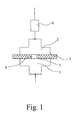
- an overvoltage protection element according to the invention is only with regard to its basic structure shown.
- To the illustrated overvoltage protection element include a first electrode 1, a second electrode 2, an ignition element 3 arranged between the two electrodes 1 and 2 and an existing between the two electrodes 1 and 2 or effective Air Punch Spark gap 4.
- an Air Punch Spark gap 4 arises between the two electrodes 1 and 2 - not illustrated - arc over which the derived lightning current flows.
- the ignition element 3 is now arranged so that between the two electrodes 1 and 2 an area of weakened insulation (ignition area) is formed, in the case of igniting the air breakdown spark gap 4 of the arc arises.
- the ignition element 3 is designed so that when concerns a voltage on the ignition element 3, a discharge on the surface 5 of the ignition element 3 to a conductive connection between the two Leads electrodes 1 and 2, wherein the conductive compound only a small Current carrying capacity. Now start over this conductive connection a leakage current to flow, so it comes because of the low current carrying capacity the conductive connection to a burning of the conductive connection and thus to an ionization of the ignition area, resulting in a abrupt ignition of the air breakdown spark gap 4 leads.
- the actual overvoltage protection element an additional voltage switching element 6, for example a varistor and / or a gas-filled surge arrester in Series switched.
- the voltage switching element 6 is so dimensioned that it is at the response voltage of the overvoltage protection device becomes conductive.
- the overvoltage protection device Occurs at the overvoltage protection device one Overvoltage, this leads to a switching of the voltage switching element 6, so that then the overvoltage is applied to the two electrodes 1 and 2, resulting in the above-described ignition of the air breakdown spark gap 4 due to the ignition triggered by the ignition of the ignition element 3 leads.
- the voltage switching element prevents 6, that normally, d. H. if there is no overvoltage, a - then unwanted - current through the overvoltage protection element flows.
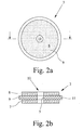
- the ignition element 3 shown in FIGS. 2 to 4 consists of two conductive Layers 7, 8 and an insulating layer 9 arranged between them, wherein the area of weakened insulation through a recess 10 in the insulating layer 9 is realized.
- the recess for example, according to 1 and 3 may be formed as a central hole, can easily through Drilling or milling are made. It can - as a comparison 2 and 4 shows - the recess 10 either only in a conductive Layer 7 or be formed in two conductive layers 7, 8.
- the production of the ignition element 3 according to the invention is now particularly special simply, that of producing multilayer printed circuit boards (Multilayer printed circuit boards) known manufacturing processes are applied can.
- the conductive layers 7, 8, which may be for example to act standardized copper foils, with the insulating Layer 9 are connected by lamination.
- the insulating Layer 9 are suitable for the production of multilayer printed circuit boards known materials, such as polyimide films or FR-4 films, with their standard available thicknesses of 35 to 100 ⁇ m. This allows the distance between the directly with the electrodes 1 and 2 Connectable conductive layers 7, 8 very low but still very accurate can be adjusted, whereby very low threshold voltages can be realized are.
- the insulating layer 9 has a slight larger outer diameter than the conductive layers 7, 8, so that on Edge region 11 of the ignition element 3 by an extended creepage distance a Increased insulation is given, which prevents ignition in this area becomes.
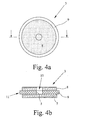
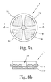
- Fig. 5 shows an embodiment of a firing element 3, the more conductive Layers 7, 8 and a plurality of insulating layers 9 has.
- the three conductive layers 7, 7 'and 7 "and the three conductive layers 8, 8 'and 8" are electrically connected to each other connected so that, although a total of six conductive layers 7, 7 ', 7 “and 8, 8 ', 8 "are present, but these have only two different potentials, wherein the two potentials are arranged alternately to each other and each separated by an insulating layer 9.
- the ignition element 3 can manufacture variations due to the properties of the insulating layers 9 and thereby conditional Fluctuations in the response voltage of the ignition element 3 balanced become.
- the initial ignition is always from the sectionzündelement 3 ' triggered that has the lowest operating voltage, d. H. otherwise same properties in the sectionzündelement 3 'with the thinnest insulating Layer 9.
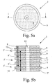
- the ignition element 3 a plurality of conductive layers 7, 7 ', 8, 8' and a plurality of insulating layers 9 on, wherein the conductive layers 7, 7 'and 8, 8' electrically connected to each other are, so that there are only two different potentials here.
- the two different potentials do not alternate several times arranged.
- the advantage of this embodiment compared to the embodiment As shown in FIG. 2 is that after the ignition of the air breakdown spark gap 4 of the arc directly on the outside conductive Layers 7, 8 skips so that a larger arc is present.
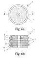
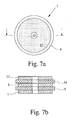
- FIGS. 7 and 8 show two embodiments of an ignition element 3 with three horizontally one above the other (Fig. 7) and four horizontally next to each other arranged potentials (Fig. 8).
- Such ignition elements 3 are suitable
- the ignition element 3 of FIG. 7 a third conductive layer 13 provided by the second conductive Layer 8 is separated by a second insulating layer 14, so that the three conductive layers 7, 8, 13 have three different potentials.
- conductive layers 8, 13, 15 and 16 are provided, each electrically not connected to each other.
- the conductive layers 8, 13, 15 and 16 are each formed like a circle segment and side by side arranged, with the circular conductive layer 7 opposite to all is arranged.
- For a pending overvoltage between the first conductive layer 7 and one of the other conductive layers 8, 13, 15 or 16 it comes first to an initial spark of the respective Air breakdown spark gap 4, due to the arrangement of the individual conductive layers 8, 13, 15 and 16 to each other or to the conductive Layer 7 is an ignition of all air breakdown spark gap 4.
- the desired level of protection not only between the active phase conductors (L1, L2, L3) and the neutral conductor (N) or between the neutral conductor (N) and earth (PE) but ensured between all lines.
Landscapes
- Emergency Protection Circuit Devices (AREA)
- Thermistors And Varistors (AREA)
Applications Claiming Priority (2)
| Application Number | Priority Date | Filing Date | Title |
|---|---|---|---|
| DE102004009072A DE102004009072A1 (de) | 2004-02-23 | 2004-02-23 | Überspannungsschutzelement und Zündelement für ein Überspannungsschutzelement |
| DE102004009072 | 2004-02-23 |
Publications (3)
| Publication Number | Publication Date |
|---|---|
| EP1566868A2 true EP1566868A2 (fr) | 2005-08-24 |
| EP1566868A3 EP1566868A3 (fr) | 2007-05-16 |
| EP1566868B1 EP1566868B1 (fr) | 2009-12-09 |
Family
ID=34706908
Family Applications (1)
| Application Number | Title | Priority Date | Filing Date |
|---|---|---|---|
| EP05003261A Expired - Lifetime EP1566868B1 (fr) | 2004-02-23 | 2005-02-16 | Dispositif dérivateur de surtensions et dispositif d'allumage pour dispositif dérivateur de surtensions |
Country Status (5)
| Country | Link |
|---|---|
| US (1) | US7817395B2 (fr) |
| EP (1) | EP1566868B1 (fr) |
| CN (1) | CN1674375B (fr) |
| DE (2) | DE102004009072A1 (fr) |
| ES (1) | ES2337695T3 (fr) |
Cited By (1)
| Publication number | Priority date | Publication date | Assignee | Title |
|---|---|---|---|---|
| DE102014102065A1 (de) | 2014-02-18 | 2015-08-20 | Phoenix Contact Gmbh & Co. Kg | Zündelement zur Verwendung bei einem Überspannungsschutzelement |
Families Citing this family (27)
| Publication number | Priority date | Publication date | Assignee | Title |
|---|---|---|---|---|
| DE102007015364B4 (de) * | 2006-12-12 | 2016-10-20 | Phoenix Contact Gmbh & Co. Kg | Überspannungsschutzeinrichtung |
| CN101378178B (zh) * | 2007-10-16 | 2012-05-30 | 曾献昌 | 带外接触发端子的多间隙金属陶瓷气体放电管 |
| DE102009048045B4 (de) | 2009-10-02 | 2011-06-01 | Phoenix Contact Gmbh & Co. Kg | Überspannungsschutzelement |
| DE202009014000U1 (de) | 2009-10-15 | 2011-02-24 | Phoenix Contact Gmbh & Co. Kg | Überspannungsschutzelement |
| DE102011102937B4 (de) | 2010-08-17 | 2017-03-02 | DEHN + SÖHNE GmbH + Co. KG. | Anordnung zur Zündung von Funkenstrecken |
| WO2012139287A1 (fr) * | 2011-04-13 | 2012-10-18 | 上海电科电器科技有限公司 | Élément de génération d'un arc déclenché |
| DE102011052803A1 (de) * | 2011-08-18 | 2013-02-21 | Phoenix Contact Gmbh & Co. Kg | Basiselement zur Aufnahme eines Überspannungsschutzmoduls |
| TWI419631B (zh) * | 2011-12-05 | 2013-12-11 | Au Optronics Corp | 多層電路板以及靜電放電保護結構 |
| DE102012002962A1 (de) | 2012-02-16 | 2013-08-22 | Phoenix Contact Gmbh & Co. Kg | Kurzschließeinrichtung zum Sach- und Personenschutz in elektrischen Systemen |
| CN102969654A (zh) * | 2012-12-18 | 2013-03-13 | 深圳市莱普斯科技有限公司 | 带熄弧栅的气体放电隙 |
| DE102013225835B4 (de) | 2013-12-13 | 2022-10-06 | Phoenix Contact Gmbh & Co. Kg | Reihenfunkenstrecke |
| DE202015100397U1 (de) * | 2015-01-28 | 2016-05-02 | Phoenix Contatct GmbH & Co. KG | Funkenstrecke mit adaptiver Kühl- und/oder Dämpfungseinrichtung |
| DE102014210516C5 (de) * | 2014-06-03 | 2020-03-26 | Phoenix Contact Gmbh & Co. Kg | Funkenstrecke |
| DE102014215279A1 (de) | 2014-08-04 | 2016-02-04 | Phoenix Contact Gmbh & Co. Kg | Schmelzsicherung für eine zu schützende Einrichtung |
| US10319545B2 (en) | 2016-11-30 | 2019-06-11 | Iskra Za{hacek over (s)}{hacek over (c)}ite d.o.o. | Surge protective device modules and DIN rail device systems including same |
| US10447026B2 (en) | 2016-12-23 | 2019-10-15 | Ripd Ip Development Ltd | Devices for active overvoltage protection |
| CZ2017143A3 (cs) * | 2017-03-15 | 2018-08-08 | Saltek S.R.O. | Omezovač napětí s přepěťovou ochranou |
| US10685767B2 (en) * | 2017-09-14 | 2020-06-16 | Raycap IP Development Ltd | Surge protective device modules and systems including same |
| US20190207386A1 (en) * | 2018-01-04 | 2019-07-04 | Ceramate Technical Co., Ltd. | Surge protection device structure |
| BE1026431B1 (de) | 2018-06-28 | 2020-02-03 | Phoenix Contact Gmbh & Co | Funkenstrecke mit Zündkreis und Funkenstreckenanordnung |
| US11223200B2 (en) | 2018-07-26 | 2022-01-11 | Ripd Ip Development Ltd | Surge protective devices, circuits, modules and systems including same |
| DE102019101448B3 (de) | 2018-10-15 | 2020-01-23 | Dehn Se + Co Kg | Anordnung zur Zündung von Funkenstrecken |
| US11862967B2 (en) | 2021-09-13 | 2024-01-02 | Raycap, S.A. | Surge protective device assembly modules |
| US11990745B2 (en) | 2022-01-12 | 2024-05-21 | Raycap IP Development Ltd | Methods and systems for remote monitoring of surge protective devices |
| US12199412B2 (en) | 2022-06-02 | 2025-01-14 | Ripd Ip Development Ltd. | Surge protective devices, circuits, modules and systems including same |
| US12206234B2 (en) | 2022-09-20 | 2025-01-21 | Ripd Ip Development Ltd | Overvoltage protection device modules |
| US12437906B2 (en) | 2022-10-18 | 2025-10-07 | Raycap, S.A. | Surge protective devices |
Family Cites Families (16)
| Publication number | Priority date | Publication date | Assignee | Title |
|---|---|---|---|---|
| AT77683B (de) * | 1917-04-16 | 1919-08-11 | Robert Bosch Ag Fa | Löschfunkenstrecke für tönende Funken. |
| GB545677A (en) * | 1940-02-29 | 1942-06-08 | Westinghouse Electric Int Co | Improvements in or relating to low voltage protective electric discharge devices |
| DE1911424A1 (de) * | 1969-03-06 | 1970-09-24 | Siemens Ag | Verfahren zum Bearbeiten von Werkstuecken mittels Unterwasser-Druckstoessen |
| US3627905A (en) * | 1969-12-08 | 1971-12-14 | British Railways Board | High-voltage electrical insulator having a predetermined surface conductance |
| CH516878A (de) * | 1970-09-18 | 1971-12-15 | Sprecher & Schuh Ag | Funkenstrecke konstanter Ansprechspannung |
| DE2337743C3 (de) * | 1973-07-25 | 1981-01-15 | Dehn + Soehne Gmbh + Co Kg, 8500 Nuernberg | Funkenstrecke |
| JPH0246680A (ja) * | 1988-08-05 | 1990-02-16 | Okaya Electric Ind Co Ltd | サージ吸収素子 |
| DE4141681C2 (de) * | 1991-12-17 | 1996-11-14 | Phoenix Contact Gmbh & Co | Überspannungsschutzelement |
| DE4244051C2 (de) * | 1992-12-28 | 1996-03-14 | Phoenix Contact Gmbh & Co | Überspannungsschutzelement |
| DE4402615C3 (de) * | 1993-05-31 | 2000-01-05 | Phoenix Contact Gmbh & Co | Überspannungsschutzelement |
| JP2888754B2 (ja) * | 1993-05-31 | 1999-05-10 | フェニックス、コンタクト、ゲゼルシャフト、ミット、ベシュレンクテル、ハフツング、ウント、コンパニー | 過電圧保護装置 |
| US5714794A (en) * | 1995-04-18 | 1998-02-03 | Hitachi Chemical Company, Ltd. | Electrostatic protective device |
| DE19741658A1 (de) * | 1997-09-16 | 1999-03-18 | Siemens Ag | Gasgefüllte Entladungsstrecke |
| DE19803636A1 (de) * | 1998-02-02 | 1999-08-05 | Phoenix Contact Gmbh & Co | Überspannungsschutzsystem |
| DE19856939A1 (de) | 1998-12-10 | 2000-06-15 | Bettermann Obo Gmbh & Co Kg | Schaltungsanordnung zum Schutz von elektrischen Installationen gegen Überspannungsereignisse |
| DE20020771U1 (de) * | 2000-02-22 | 2001-02-15 | Dehn & Soehne | Druckfest gekapselte Funkenstreckenanordnung zum Ableiten von schädlichen Störgrößen durch Überspannung |
-
2004
- 2004-02-23 DE DE102004009072A patent/DE102004009072A1/de not_active Withdrawn
-
2005
- 2005-02-16 ES ES05003261T patent/ES2337695T3/es not_active Expired - Lifetime
- 2005-02-16 EP EP05003261A patent/EP1566868B1/fr not_active Expired - Lifetime
- 2005-02-16 DE DE502005008658T patent/DE502005008658D1/de not_active Expired - Lifetime
- 2005-02-23 US US11/062,636 patent/US7817395B2/en not_active Expired - Lifetime
- 2005-02-23 CN CN2005100565544A patent/CN1674375B/zh not_active Expired - Lifetime
Cited By (2)
| Publication number | Priority date | Publication date | Assignee | Title |
|---|---|---|---|---|
| DE102014102065A1 (de) | 2014-02-18 | 2015-08-20 | Phoenix Contact Gmbh & Co. Kg | Zündelement zur Verwendung bei einem Überspannungsschutzelement |
| WO2015124624A1 (fr) | 2014-02-18 | 2015-08-27 | Phoenix Contact Gmbh & Co. Kg | Élément d'allumage destiné à être utilisé dans un élément de protection contre les surtensions |
Also Published As
| Publication number | Publication date |
|---|---|
| ES2337695T3 (es) | 2010-04-28 |
| US20050185356A1 (en) | 2005-08-25 |
| DE102004009072A1 (de) | 2005-09-08 |
| DE502005008658D1 (de) | 2010-01-21 |
| CN1674375B (zh) | 2011-12-21 |
| CN1674375A (zh) | 2005-09-28 |
| US7817395B2 (en) | 2010-10-19 |
| EP1566868A3 (fr) | 2007-05-16 |
| EP1566868B1 (fr) | 2009-12-09 |
Similar Documents
| Publication | Publication Date | Title |
|---|---|---|
| EP1566868B1 (fr) | Dispositif dérivateur de surtensions et dispositif d'allumage pour dispositif dérivateur de surtensions | |
| EP0933860B1 (fr) | Système de protection contre les surtensions | |
| EP0815454B1 (fr) | Transformateur de tension | |
| DE102012022399A1 (de) | Zündkreis | |
| EP1456921B1 (fr) | Dispositif de protection contre les surtensions | |
| EP1423894B1 (fr) | Dispositif de protection contre les surtensions | |
| EP1461852B1 (fr) | Systeme multipolaire de protection contre les surtensions et procede de fonctionnement fiable d'un systeme multipolaire de protection contre les surtensions | |
| DE10146728B4 (de) | Überspannungsschutzeinrichtung | |
| DE4244051C2 (de) | Überspannungsschutzelement | |
| EP1692751A1 (fr) | Dispositif de protection contre les surtensions | |
| DE19707769A1 (de) | Einrichtung zum Schutz von elektrischen Schaltungen, insbesondere der Automobiltechnik, vor elektrostatischen Entladungen | |
| DE19914313A1 (de) | Überspannungsschutzsystem | |
| DE4141682A1 (de) | Ueberspannungsschutzelement | |
| EP3834260B1 (fr) | Ensemble d'amorçage d'éclateurs | |
| DE3910435C2 (fr) | ||
| EP2876653B1 (fr) | Élément multicontact pour un varistor | |
| CH668516A5 (de) | Ueberspannungsschutzeinrichtung fuer elektrische anlagen, insbesondere fuer elektronische apparate. | |
| DE102014102065B4 (de) | Zündelement zur Verwendung bei einem Überspannungsschutzelement, Überspannungsschutzelement und Verfahren zur Herstellung eines Zündelements | |
| DE102015200186A1 (de) | Überspannungsschutzvorrichtung sowie Leuchte mit einer derartigen Überspannungsschutzvorrichtung | |
| EP3588706B1 (fr) | Dispositif d'éclateur avec deux circuits d'allumage | |
| DE3037120A1 (de) | Ueberspannungsschutzschaltung mit zenerdiode | |
| DE102009049579A1 (de) | Überspannungschutzeinrichtung | |
| DE102007015364A1 (de) | Überspannungsschutzeinrichtung | |
| EP4270688B1 (fr) | Éclateur multiple | |
| AT17235U1 (de) | Leiterplatte mit Schutzelement |
Legal Events
| Date | Code | Title | Description |
|---|---|---|---|
| PUAI | Public reference made under article 153(3) epc to a published international application that has entered the european phase |
Free format text: ORIGINAL CODE: 0009012 |
|
| AK | Designated contracting states |
Kind code of ref document: A2 Designated state(s): AT BE BG CH CY CZ DE DK EE ES FI FR GB GR HU IE IS IT LI LT LU MC NL PL PT RO SE SI SK TR |
|
| AX | Request for extension of the european patent |
Extension state: AL BA HR LV MK YU |
|
| PUAL | Search report despatched |
Free format text: ORIGINAL CODE: 0009013 |
|
| AK | Designated contracting states |
Kind code of ref document: A3 Designated state(s): AT BE BG CH CY CZ DE DK EE ES FI FR GB GR HU IE IS IT LI LT LU MC NL PL PT RO SE SI SK TR |
|
| AX | Request for extension of the european patent |
Extension state: AL BA HR LV MK YU |
|
| 17P | Request for examination filed |
Effective date: 20070718 |
|
| 17Q | First examination report despatched |
Effective date: 20070830 |
|
| AKX | Designation fees paid |
Designated state(s): DE ES FR IT SE |
|
| GRAP | Despatch of communication of intention to grant a patent |
Free format text: ORIGINAL CODE: EPIDOSNIGR1 |
|
| GRAS | Grant fee paid |
Free format text: ORIGINAL CODE: EPIDOSNIGR3 |
|
| GRAA | (expected) grant |
Free format text: ORIGINAL CODE: 0009210 |
|
| AK | Designated contracting states |
Kind code of ref document: B1 Designated state(s): DE ES FR IT SE |
|
| REF | Corresponds to: |
Ref document number: 502005008658 Country of ref document: DE Date of ref document: 20100121 Kind code of ref document: P |
|
| REG | Reference to a national code |
Ref country code: SE Ref legal event code: TRGR |
|
| REG | Reference to a national code |
Ref country code: ES Ref legal event code: FG2A Ref document number: 2337695 Country of ref document: ES Kind code of ref document: T3 |
|
| PLBE | No opposition filed within time limit |
Free format text: ORIGINAL CODE: 0009261 |
|
| STAA | Information on the status of an ep patent application or granted ep patent |
Free format text: STATUS: NO OPPOSITION FILED WITHIN TIME LIMIT |
|
| 26N | No opposition filed |
Effective date: 20100910 |
|
| PGFP | Annual fee paid to national office [announced via postgrant information from national office to epo] |
Ref country code: IT Payment date: 20150225 Year of fee payment: 11 |
|
| PGFP | Annual fee paid to national office [announced via postgrant information from national office to epo] |
Ref country code: SE Payment date: 20150220 Year of fee payment: 11 |
|
| REG | Reference to a national code |
Ref country code: FR Ref legal event code: PLFP Year of fee payment: 12 |
|
| PGFP | Annual fee paid to national office [announced via postgrant information from national office to epo] |
Ref country code: ES Payment date: 20160201 Year of fee payment: 12 |
|
| REG | Reference to a national code |
Ref country code: SE Ref legal event code: EUG |
|
| PG25 | Lapsed in a contracting state [announced via postgrant information from national office to epo] |
Ref country code: SE Free format text: LAPSE BECAUSE OF NON-PAYMENT OF DUE FEES Effective date: 20160217 |
|
| PG25 | Lapsed in a contracting state [announced via postgrant information from national office to epo] |
Ref country code: IT Free format text: LAPSE BECAUSE OF NON-PAYMENT OF DUE FEES Effective date: 20160216 |
|
| REG | Reference to a national code |
Ref country code: FR Ref legal event code: PLFP Year of fee payment: 13 |
|
| REG | Reference to a national code |
Ref country code: FR Ref legal event code: PLFP Year of fee payment: 14 |
|
| REG | Reference to a national code |
Ref country code: ES Ref legal event code: FD2A Effective date: 20180704 |
|
| PG25 | Lapsed in a contracting state [announced via postgrant information from national office to epo] |
Ref country code: ES Free format text: LAPSE BECAUSE OF NON-PAYMENT OF DUE FEES Effective date: 20170217 |
|
| PGFP | Annual fee paid to national office [announced via postgrant information from national office to epo] |
Ref country code: FR Payment date: 20200225 Year of fee payment: 16 |
|
| PG25 | Lapsed in a contracting state [announced via postgrant information from national office to epo] |
Ref country code: FR Free format text: LAPSE BECAUSE OF NON-PAYMENT OF DUE FEES Effective date: 20210228 |
|
| P01 | Opt-out of the competence of the unified patent court (upc) registered |
Effective date: 20230424 |
|
| PGFP | Annual fee paid to national office [announced via postgrant information from national office to epo] |
Ref country code: DE Payment date: 20240429 Year of fee payment: 20 |
|
| REG | Reference to a national code |
Ref country code: DE Ref legal event code: R071 Ref document number: 502005008658 Country of ref document: DE |