EP1548833A1 - Ferroelektrischer speicher und verfahren zu seiner herstellung - Google Patents
Ferroelektrischer speicher und verfahren zu seiner herstellung Download PDFInfo
- Publication number
- EP1548833A1 EP1548833A1 EP03788099A EP03788099A EP1548833A1 EP 1548833 A1 EP1548833 A1 EP 1548833A1 EP 03788099 A EP03788099 A EP 03788099A EP 03788099 A EP03788099 A EP 03788099A EP 1548833 A1 EP1548833 A1 EP 1548833A1
- Authority
- EP
- European Patent Office
- Prior art keywords
- substrate
- cell array
- ferroelectric
- memory cell
- sheet
- Prior art date
- Legal status (The legal status is an assumption and is not a legal conclusion. Google has not performed a legal analysis and makes no representation as to the accuracy of the status listed.)
- Withdrawn
Links
Images


Classifications
-
- G—PHYSICS
- G11—INFORMATION STORAGE
- G11C—STATIC STORES
- G11C11/00—Digital stores characterised by the use of particular electric or magnetic storage elements; Storage elements therefor
- G11C11/21—Digital stores characterised by the use of particular electric or magnetic storage elements; Storage elements therefor using electric elements
- G11C11/22—Digital stores characterised by the use of particular electric or magnetic storage elements; Storage elements therefor using electric elements using ferroelectric elements
-
- H—ELECTRICITY
- H10—SEMICONDUCTOR DEVICES; ELECTRIC SOLID-STATE DEVICES NOT OTHERWISE PROVIDED FOR
- H10D—INORGANIC ELECTRIC SEMICONDUCTOR DEVICES
- H10D86/00—Integrated devices formed in or on insulating or conducting substrates, e.g. formed in silicon-on-insulator [SOI] substrates or on stainless steel or glass substrates
- H10D86/01—Manufacture or treatment
-
- H—ELECTRICITY
- H10—SEMICONDUCTOR DEVICES; ELECTRIC SOLID-STATE DEVICES NOT OTHERWISE PROVIDED FOR
- H10D—INORGANIC ELECTRIC SEMICONDUCTOR DEVICES
- H10D86/00—Integrated devices formed in or on insulating or conducting substrates, e.g. formed in silicon-on-insulator [SOI] substrates or on stainless steel or glass substrates
- H10D86/201—Integrated devices formed in or on insulating or conducting substrates, e.g. formed in silicon-on-insulator [SOI] substrates or on stainless steel or glass substrates the substrates comprising an insulating layer on a semiconductor body, e.g. SOI
-
- H—ELECTRICITY
- H10—SEMICONDUCTOR DEVICES; ELECTRIC SOLID-STATE DEVICES NOT OTHERWISE PROVIDED FOR
- H10P—GENERIC PROCESSES OR APPARATUS FOR THE MANUFACTURE OR TREATMENT OF DEVICES COVERED BY CLASS H10
- H10P72/00—Handling or holding of wafers, substrates or devices during manufacture or treatment thereof
- H10P72/70—Handling or holding of wafers, substrates or devices during manufacture or treatment thereof for supporting or gripping
- H10P72/74—Handling or holding of wafers, substrates or devices during manufacture or treatment thereof for supporting or gripping using temporarily an auxiliary support
-
- H—ELECTRICITY
- H10—SEMICONDUCTOR DEVICES; ELECTRIC SOLID-STATE DEVICES NOT OTHERWISE PROVIDED FOR
- H10W—GENERIC PACKAGES, INTERCONNECTIONS, CONNECTORS OR OTHER CONSTRUCTIONAL DETAILS OF DEVICES COVERED BY CLASS H10
- H10W90/00—Package configurations
-
- H—ELECTRICITY
- H10—SEMICONDUCTOR DEVICES; ELECTRIC SOLID-STATE DEVICES NOT OTHERWISE PROVIDED FOR
- H10B—ELECTRONIC MEMORY DEVICES
- H10B53/00—Ferroelectric RAM [FeRAM] devices comprising ferroelectric memory capacitors
-
- H—ELECTRICITY
- H10—SEMICONDUCTOR DEVICES; ELECTRIC SOLID-STATE DEVICES NOT OTHERWISE PROVIDED FOR
- H10P—GENERIC PROCESSES OR APPARATUS FOR THE MANUFACTURE OR TREATMENT OF DEVICES COVERED BY CLASS H10
- H10P72/00—Handling or holding of wafers, substrates or devices during manufacture or treatment thereof
- H10P72/70—Handling or holding of wafers, substrates or devices during manufacture or treatment thereof for supporting or gripping
- H10P72/74—Handling or holding of wafers, substrates or devices during manufacture or treatment thereof for supporting or gripping using temporarily an auxiliary support
- H10P72/7426—Handling or holding of wafers, substrates or devices during manufacture or treatment thereof for supporting or gripping using temporarily an auxiliary support used as a support during build up manufacturing of active devices
-
- H—ELECTRICITY
- H10—SEMICONDUCTOR DEVICES; ELECTRIC SOLID-STATE DEVICES NOT OTHERWISE PROVIDED FOR
- H10P—GENERIC PROCESSES OR APPARATUS FOR THE MANUFACTURE OR TREATMENT OF DEVICES COVERED BY CLASS H10
- H10P72/00—Handling or holding of wafers, substrates or devices during manufacture or treatment thereof
- H10P72/70—Handling or holding of wafers, substrates or devices during manufacture or treatment thereof for supporting or gripping
- H10P72/74—Handling or holding of wafers, substrates or devices during manufacture or treatment thereof for supporting or gripping using temporarily an auxiliary support
- H10P72/743—Handling or holding of wafers, substrates or devices during manufacture or treatment thereof for supporting or gripping using temporarily an auxiliary support used as a support during manufacture of interconnect decals or build up layers
-
- H—ELECTRICITY
- H10—SEMICONDUCTOR DEVICES; ELECTRIC SOLID-STATE DEVICES NOT OTHERWISE PROVIDED FOR
- H10P—GENERIC PROCESSES OR APPARATUS FOR THE MANUFACTURE OR TREATMENT OF DEVICES COVERED BY CLASS H10
- H10P72/00—Handling or holding of wafers, substrates or devices during manufacture or treatment thereof
- H10P72/70—Handling or holding of wafers, substrates or devices during manufacture or treatment thereof for supporting or gripping
- H10P72/74—Handling or holding of wafers, substrates or devices during manufacture or treatment thereof for supporting or gripping using temporarily an auxiliary support
- H10P72/7432—Handling or holding of wafers, substrates or devices during manufacture or treatment thereof for supporting or gripping using temporarily an auxiliary support used in a transfer process involving transfer directly from an origin substrate to a target substrate without use of an intermediate handle substrate
-
- H—ELECTRICITY
- H10—SEMICONDUCTOR DEVICES; ELECTRIC SOLID-STATE DEVICES NOT OTHERWISE PROVIDED FOR
- H10W—GENERIC PACKAGES, INTERCONNECTIONS, CONNECTORS OR OTHER CONSTRUCTIONAL DETAILS OF DEVICES COVERED BY CLASS H10
- H10W72/00—Interconnections or connectors in packages
- H10W72/071—Connecting or disconnecting
- H10W72/073—Connecting or disconnecting of die-attach connectors
-
- H—ELECTRICITY
- H10—SEMICONDUCTOR DEVICES; ELECTRIC SOLID-STATE DEVICES NOT OTHERWISE PROVIDED FOR
- H10W—GENERIC PACKAGES, INTERCONNECTIONS, CONNECTORS OR OTHER CONSTRUCTIONAL DETAILS OF DEVICES COVERED BY CLASS H10
- H10W72/00—Interconnections or connectors in packages
- H10W72/851—Dispositions of multiple connectors or interconnections
- H10W72/874—On different surfaces
- H10W72/884—Die-attach connectors and bond wires
-
- H—ELECTRICITY
- H10—SEMICONDUCTOR DEVICES; ELECTRIC SOLID-STATE DEVICES NOT OTHERWISE PROVIDED FOR
- H10W—GENERIC PACKAGES, INTERCONNECTIONS, CONNECTORS OR OTHER CONSTRUCTIONAL DETAILS OF DEVICES COVERED BY CLASS H10
- H10W90/00—Package configurations
- H10W90/20—Configurations of stacked chips
- H10W90/22—Configurations of stacked chips the stacked chips being on both top and bottom sides of a package substrate, interposer or RDL
-
- H—ELECTRICITY
- H10—SEMICONDUCTOR DEVICES; ELECTRIC SOLID-STATE DEVICES NOT OTHERWISE PROVIDED FOR
- H10W—GENERIC PACKAGES, INTERCONNECTIONS, CONNECTORS OR OTHER CONSTRUCTIONAL DETAILS OF DEVICES COVERED BY CLASS H10
- H10W90/00—Package configurations
- H10W90/20—Configurations of stacked chips
- H10W90/26—Configurations of stacked chips the stacked chips being of the same size without any chips being laterally offset, e.g. chip stacks having a rectangular shape
-
- H—ELECTRICITY
- H10—SEMICONDUCTOR DEVICES; ELECTRIC SOLID-STATE DEVICES NOT OTHERWISE PROVIDED FOR
- H10W—GENERIC PACKAGES, INTERCONNECTIONS, CONNECTORS OR OTHER CONSTRUCTIONAL DETAILS OF DEVICES COVERED BY CLASS H10
- H10W90/00—Package configurations
- H10W90/20—Configurations of stacked chips
- H10W90/28—Configurations of stacked chips the stacked chips having different sizes, e.g. chip stacks having a pyramidal shape
-
- H—ELECTRICITY
- H10—SEMICONDUCTOR DEVICES; ELECTRIC SOLID-STATE DEVICES NOT OTHERWISE PROVIDED FOR
- H10W—GENERIC PACKAGES, INTERCONNECTIONS, CONNECTORS OR OTHER CONSTRUCTIONAL DETAILS OF DEVICES COVERED BY CLASS H10
- H10W90/00—Package configurations
- H10W90/20—Configurations of stacked chips
- H10W90/297—Configurations of stacked chips characterised by the through-semiconductor vias [TSVs] in the stacked chips
-
- H—ELECTRICITY
- H10—SEMICONDUCTOR DEVICES; ELECTRIC SOLID-STATE DEVICES NOT OTHERWISE PROVIDED FOR
- H10W—GENERIC PACKAGES, INTERCONNECTIONS, CONNECTORS OR OTHER CONSTRUCTIONAL DETAILS OF DEVICES COVERED BY CLASS H10
- H10W90/00—Package configurations
- H10W90/701—Package configurations characterised by the relative positions of pads or connectors relative to package parts
- H10W90/721—Package configurations characterised by the relative positions of pads or connectors relative to package parts of bump connectors
- H10W90/722—Package configurations characterised by the relative positions of pads or connectors relative to package parts of bump connectors between stacked chips
-
- H—ELECTRICITY
- H10—SEMICONDUCTOR DEVICES; ELECTRIC SOLID-STATE DEVICES NOT OTHERWISE PROVIDED FOR
- H10W—GENERIC PACKAGES, INTERCONNECTIONS, CONNECTORS OR OTHER CONSTRUCTIONAL DETAILS OF DEVICES COVERED BY CLASS H10
- H10W90/00—Package configurations
- H10W90/701—Package configurations characterised by the relative positions of pads or connectors relative to package parts
- H10W90/721—Package configurations characterised by the relative positions of pads or connectors relative to package parts of bump connectors
- H10W90/724—Package configurations characterised by the relative positions of pads or connectors relative to package parts of bump connectors between a chip and a stacked insulating package substrate, interposer or RDL
-
- H—ELECTRICITY
- H10—SEMICONDUCTOR DEVICES; ELECTRIC SOLID-STATE DEVICES NOT OTHERWISE PROVIDED FOR
- H10W—GENERIC PACKAGES, INTERCONNECTIONS, CONNECTORS OR OTHER CONSTRUCTIONAL DETAILS OF DEVICES COVERED BY CLASS H10
- H10W90/00—Package configurations
- H10W90/701—Package configurations characterised by the relative positions of pads or connectors relative to package parts
- H10W90/731—Package configurations characterised by the relative positions of pads or connectors relative to package parts of die-attach connectors
- H10W90/732—Package configurations characterised by the relative positions of pads or connectors relative to package parts of die-attach connectors between stacked chips
-
- H—ELECTRICITY
- H10—SEMICONDUCTOR DEVICES; ELECTRIC SOLID-STATE DEVICES NOT OTHERWISE PROVIDED FOR
- H10W—GENERIC PACKAGES, INTERCONNECTIONS, CONNECTORS OR OTHER CONSTRUCTIONAL DETAILS OF DEVICES COVERED BY CLASS H10
- H10W90/00—Package configurations
- H10W90/701—Package configurations characterised by the relative positions of pads or connectors relative to package parts
- H10W90/731—Package configurations characterised by the relative positions of pads or connectors relative to package parts of die-attach connectors
- H10W90/734—Package configurations characterised by the relative positions of pads or connectors relative to package parts of die-attach connectors between a chip and a stacked insulating package substrate, interposer or RDL
-
- H—ELECTRICITY
- H10—SEMICONDUCTOR DEVICES; ELECTRIC SOLID-STATE DEVICES NOT OTHERWISE PROVIDED FOR
- H10W—GENERIC PACKAGES, INTERCONNECTIONS, CONNECTORS OR OTHER CONSTRUCTIONAL DETAILS OF DEVICES COVERED BY CLASS H10
- H10W90/00—Package configurations
- H10W90/701—Package configurations characterised by the relative positions of pads or connectors relative to package parts
- H10W90/751—Package configurations characterised by the relative positions of pads or connectors relative to package parts of bond wires
- H10W90/754—Package configurations characterised by the relative positions of pads or connectors relative to package parts of bond wires between a chip and a stacked insulating package substrate, interposer or RDL
Definitions
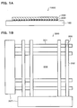
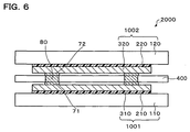
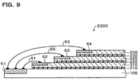
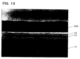
- the lower electrodes 301 function as word lines for selecting rows, and the upper electrodes 302 function as bit lines for selecting columns.
- the lower electrodes 301 and the upper electrodes 302 may be formed so that the lower electrodes 301 function as the word lines and the upper electrodes 302 function as the bit lines.
- the peripheral circuit section 307 has at least a function of writing information in each memory cell of the memory cell array 304 and reading information from each memory cell.
- the peripheral circuit section 307 includes a driver circuit and a signal detection circuit for selectively controlling the lower electrodes 301 and the upper electrodes 302 and the like.
- a Y gate, sense amplifier, input/output buffer, X address decoder, Y address decoder, address buffer, and the like can be given.
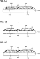
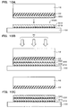
- the sheet-shaped devices 310 and 320 are multi-layered together with the flexible substrates 110 and 120, handling capability during the steps can be increased and the degree of integration can be increased by using simple steps. Moreover, according to this manufacturing method, a process which causes a large amount of load to be applied to each section of the device, such as a formation step of an interlayer dielectric or the like, can be omitted when multi-layering the sheet-shaped devices 310 and 320, whereby the sheet-shaped devices 310 and 320 can be multi-layered and integrated while securing the characteristics of the sheet-shaped devices 310 and 320.
Landscapes
- Engineering & Computer Science (AREA)
- Computer Hardware Design (AREA)
- Semiconductor Memories (AREA)
Applications Claiming Priority (3)
| Application Number | Priority Date | Filing Date | Title |
|---|---|---|---|
| JP2002238014 | 2002-08-19 | ||
| JP2002238014 | 2002-08-19 | ||
| PCT/JP2003/010306 WO2004017410A1 (ja) | 2002-08-19 | 2003-08-13 | 強誘電体メモリおよびその製造方法 |
Publications (2)
| Publication Number | Publication Date |
|---|---|
| EP1548833A1 true EP1548833A1 (de) | 2005-06-29 |
| EP1548833A4 EP1548833A4 (de) | 2007-03-21 |
Family
ID=31884449
Family Applications (1)
| Application Number | Title | Priority Date | Filing Date |
|---|---|---|---|
| EP03788099A Withdrawn EP1548833A4 (de) | 2002-08-19 | 2003-08-13 | Ferroelektrischer speicher und verfahren zu seiner herstellung |
Country Status (4)
| Country | Link |
|---|---|
| US (2) | US6917063B2 (de) |
| EP (1) | EP1548833A4 (de) |
| JP (1) | JPWO2004017410A1 (de) |
| WO (1) | WO2004017410A1 (de) |
Cited By (1)
| Publication number | Priority date | Publication date | Assignee | Title |
|---|---|---|---|---|
| EP1946374A4 (de) * | 2005-11-09 | 2014-01-01 | Semiconductor Energy Lab | Halbleitervorrichtung und herstellungsverfahren dafür |
Families Citing this family (11)
| Publication number | Priority date | Publication date | Assignee | Title |
|---|---|---|---|---|
| JP2004241632A (ja) * | 2003-02-06 | 2004-08-26 | Seiko Epson Corp | 強誘電体メモリおよびその製造方法 |
| US7057877B2 (en) * | 2003-08-27 | 2006-06-06 | Seiko Epson Corporation | Capacitor, method of manufacture thereof and semiconductor device |
| JP2005136071A (ja) * | 2003-10-29 | 2005-05-26 | Seiko Epson Corp | クロスポイント型強誘電体メモリ |
| JP4653426B2 (ja) | 2004-06-25 | 2011-03-16 | セイコーエプソン株式会社 | 半導体装置 |
| NO20052904L (no) * | 2005-06-14 | 2006-12-15 | Thin Film Electronics Asa | Et ikke-flyktig elektrisk minnesystem |
| JP4433200B2 (ja) * | 2005-12-20 | 2010-03-17 | セイコーエプソン株式会社 | 強誘電体キャパシタおよび半導体装置 |
| KR20090103113A (ko) * | 2008-03-27 | 2009-10-01 | 삼성전자주식회사 | 반도체 소자 및 그 제조방법 |
| US8455936B2 (en) * | 2010-02-25 | 2013-06-04 | Avago Technologies General Ip (Singapore) Pte. Ltd. | Configurable memory sheet and package assembly |
| US8987787B2 (en) * | 2012-04-10 | 2015-03-24 | Macronix International Co., Ltd. | Semiconductor structure and method for manufacturing the same |
| EP3123507A4 (de) * | 2014-03-27 | 2017-12-06 | Intel Corporation | Prozessintegration für flexibles elektroniksystem-on-chip (soc) mit mehreren bauelementen |
| JP7688550B2 (ja) * | 2021-09-17 | 2025-06-04 | キオクシア株式会社 | 半導体装置、半導体装置の製造方法、および基板の再利用方法 |
Family Cites Families (12)
| Publication number | Priority date | Publication date | Assignee | Title |
|---|---|---|---|---|
| JP2788265B2 (ja) * | 1988-07-08 | 1998-08-20 | オリンパス光学工業株式会社 | 強誘電体メモリ及びその駆動方法,製造方法 |
| JPH07202052A (ja) * | 1993-12-28 | 1995-08-04 | Hitachi Ltd | 半導体集積回路装置の製造方法 |
| JP3809712B2 (ja) | 1996-08-27 | 2006-08-16 | セイコーエプソン株式会社 | 薄膜デバイスの転写方法 |
| JP4085459B2 (ja) * | 1998-03-02 | 2008-05-14 | セイコーエプソン株式会社 | 3次元デバイスの製造方法 |
| JP3690135B2 (ja) * | 1998-09-10 | 2005-08-31 | セイコーエプソン株式会社 | デバイスの製造方法 |
| US6249014B1 (en) * | 1998-10-01 | 2001-06-19 | Ramtron International Corporation | Hydrogen barrier encapsulation techniques for the control of hydrogen induced degradation of ferroelectric capacitors in conjunction with multilevel metal processing for non-volatile integrated circuit memory devices |
| EP1135807A1 (de) * | 1998-12-04 | 2001-09-26 | Thin Film Electronics ASA | Skalierbare datenverarbeitungsvorrichtung |
| US6114088A (en) * | 1999-01-15 | 2000-09-05 | 3M Innovative Properties Company | Thermal transfer element for forming multilayer devices |
| JP3620041B2 (ja) * | 1999-12-09 | 2005-02-16 | セイコーエプソン株式会社 | メモリデバイス及びその製造方法、並びに電子機器 |
| JP2002026282A (ja) * | 2000-06-30 | 2002-01-25 | Seiko Epson Corp | 単純マトリクス型メモリ素子の製造方法 |
| JP2002269972A (ja) * | 2000-12-27 | 2002-09-20 | Seiko Epson Corp | 強誘電体メモリ装置および強誘電体キャパシタからなるメモリセルに対する動作方法 |
| JP2002217391A (ja) * | 2001-01-23 | 2002-08-02 | Seiko Epson Corp | 積層体の製造方法及び半導体装置 |
-
2003
- 2003-08-13 WO PCT/JP2003/010306 patent/WO2004017410A1/ja not_active Ceased
- 2003-08-13 JP JP2004528873A patent/JPWO2004017410A1/ja not_active Withdrawn
- 2003-08-13 EP EP03788099A patent/EP1548833A4/de not_active Withdrawn
- 2003-08-14 US US10/640,264 patent/US6917063B2/en not_active Expired - Fee Related
-
2005
- 2005-06-08 US US11/147,279 patent/US20050263809A1/en not_active Abandoned
Cited By (1)
| Publication number | Priority date | Publication date | Assignee | Title |
|---|---|---|---|---|
| EP1946374A4 (de) * | 2005-11-09 | 2014-01-01 | Semiconductor Energy Lab | Halbleitervorrichtung und herstellungsverfahren dafür |
Also Published As
| Publication number | Publication date |
|---|---|
| JPWO2004017410A1 (ja) | 2005-12-08 |
| US20040232458A1 (en) | 2004-11-25 |
| EP1548833A4 (de) | 2007-03-21 |
| US20050263809A1 (en) | 2005-12-01 |
| US6917063B2 (en) | 2005-07-12 |
| WO2004017410A1 (ja) | 2004-02-26 |
Similar Documents
| Publication | Publication Date | Title |
|---|---|---|
| JP4063082B2 (ja) | フレキシブル電子デバイスとその製造方法 | |
| US10672821B2 (en) | Sensor device and manufacturing method thereof | |
| JP4042182B2 (ja) | Icカードの製造方法及び薄膜集積回路装置の製造方法 | |
| US6814832B2 (en) | Method for transferring element, method for producing element, integrated circuit, circuit board, electro-optical device, IC card, and electronic appliance | |
| US6917063B2 (en) | Ferroelectric memory and method of fabricating the same | |
| US6700631B1 (en) | Method of separating thin-film device, method of transferring thin-film device, thin-film device, active matrix substrate, and liquid crystal display device | |
| JP4103421B2 (ja) | 電子デバイス及び電子機器 | |
| JPH11251518A (ja) | 3次元デバイス | |
| KR20090083362A (ko) | 반도체 디바이스 및 이의 제작 방법 | |
| JPH10125930A (ja) | 剥離方法 | |
| JP2002217391A (ja) | 積層体の製造方法及び半導体装置 | |
| JP2004172478A (ja) | 半導体装置及びその製造方法、該半導体装置に係る測定用治具 | |
| JP4061846B2 (ja) | 積層体の製造方法及び半導体装置の製造方法 | |
| US7674634B2 (en) | Method of producing semiconductor device | |
| JPH10177187A (ja) | 転写された薄膜構造ブロック間の電気的導通をとる方法,アクティブマトリクス基板の製造方法,アクティブマトリクス基板および液晶装置 | |
| CN100456476C (zh) | 强介电存储器及其制造方法 | |
| JP2004296681A (ja) | 強誘電体膜、強誘電体膜の製造方法、強誘電体キャパシタおよび強誘電体キャパシタの製造方法ならびに強誘電体メモリ | |
| JP5245029B2 (ja) | 半導体装置 | |
| JP2023179298A (ja) | 半導体デバイス及びその製造方法 | |
| JP2004241632A5 (de) | ||
| JP2006245185A (ja) | 有機強誘電体メモリ及びその製造方法 | |
| JP2006253295A (ja) | 有機強誘電体メモリ及びその製造方法 | |
| WO1992002045A1 (fr) | Procede de fabrication de dispositifs a semi-conducteurs | |
| JP2006245184A (ja) | 有機強誘電体メモリおよびその製造方法 | |
| US20080113453A1 (en) | Fabrication process of semiconductor device |
Legal Events
| Date | Code | Title | Description |
|---|---|---|---|
| PUAI | Public reference made under article 153(3) epc to a published international application that has entered the european phase |
Free format text: ORIGINAL CODE: 0009012 |
|
| 17P | Request for examination filed |
Effective date: 20050207 |
|
| AK | Designated contracting states |
Kind code of ref document: A1 Designated state(s): AT BE BG CH CY CZ DE DK EE ES FI FR GB GR HU IE IT LI LU MC NL PT RO SE SI SK TR |
|
| AX | Request for extension of the european patent |
Extension state: AL LT LV MK |
|
| DAX | Request for extension of the european patent (deleted) | ||
| RBV | Designated contracting states (corrected) |
Designated state(s): DE GB |
|
| A4 | Supplementary search report drawn up and despatched |
Effective date: 20070215 |
|
| RIC1 | Information provided on ipc code assigned before grant |
Ipc: H01L 27/115 20060101ALN20070209BHEP Ipc: H01L 27/105 20060101ALN20070209BHEP Ipc: H01L 27/12 20060101ALI20070209BHEP Ipc: H01L 21/84 20060101ALI20070209BHEP Ipc: H01L 21/68 20060101ALI20070209BHEP Ipc: H01L 21/98 20060101ALI20070209BHEP Ipc: H01L 23/48 20060101ALI20070209BHEP Ipc: H01L 25/065 20060101AFI20070209BHEP |
|
| 17Q | First examination report despatched |
Effective date: 20070503 |
|
| STAA | Information on the status of an ep patent application or granted ep patent |
Free format text: STATUS: THE APPLICATION IS DEEMED TO BE WITHDRAWN |
|
| 18D | Application deemed to be withdrawn |
Effective date: 20090526 |