EP1544991B1 - Spannungsdetektionsschaltung, Hochspannungserzeugungsschaltung, und Halbleiterspeichervorrichtung - Google Patents
Spannungsdetektionsschaltung, Hochspannungserzeugungsschaltung, und Halbleiterspeichervorrichtung Download PDFInfo
- Publication number
- EP1544991B1 EP1544991B1 EP04027818.6A EP04027818A EP1544991B1 EP 1544991 B1 EP1544991 B1 EP 1544991B1 EP 04027818 A EP04027818 A EP 04027818A EP 1544991 B1 EP1544991 B1 EP 1544991B1
- Authority
- EP
- European Patent Office
- Prior art keywords
- voltage
- control signal
- circuit
- pump
- resistor
- Prior art date
- Legal status (The legal status is an assumption and is not a legal conclusion. Google has not performed a legal analysis and makes no representation as to the accuracy of the status listed.)
- Expired - Lifetime
Links
Images





Classifications
-
- H—ELECTRICITY
- H02—GENERATION; CONVERSION OR DISTRIBUTION OF ELECTRIC POWER
- H02M—APPARATUS FOR CONVERSION BETWEEN AC AND AC, BETWEEN AC AND DC, OR BETWEEN DC AND DC, AND FOR USE WITH MAINS OR SIMILAR POWER SUPPLY SYSTEMS; CONVERSION OF DC OR AC INPUT POWER INTO SURGE OUTPUT POWER; CONTROL OR REGULATION THEREOF
- H02M3/00—Conversion of DC power input into DC power output
- H02M3/02—Conversion of DC power input into DC power output without intermediate conversion into AC
- H02M3/04—Conversion of DC power input into DC power output without intermediate conversion into AC by static converters
- H02M3/06—Conversion of DC power input into DC power output without intermediate conversion into AC by static converters using resistors or capacitors, e.g. potential divider
- H02M3/07—Conversion of DC power input into DC power output without intermediate conversion into AC by static converters using resistors or capacitors, e.g. potential divider using capacitors charged and discharged alternately by semiconductor devices with control electrode, e.g. charge pumps
- H02M3/073—Charge pumps of the Schenkel-type
-
- G—PHYSICS
- G11—INFORMATION STORAGE
- G11C—STATIC STORES
- G11C5/00—Details of stores covered by group G11C11/00
- G11C5/14—Power supply arrangements, e.g. power down, chip selection or deselection, layout of wirings or power grids, or multiple supply levels
-
- H—ELECTRICITY
- H02—GENERATION; CONVERSION OR DISTRIBUTION OF ELECTRIC POWER
- H02M—APPARATUS FOR CONVERSION BETWEEN AC AND AC, BETWEEN AC AND DC, OR BETWEEN DC AND DC, AND FOR USE WITH MAINS OR SIMILAR POWER SUPPLY SYSTEMS; CONVERSION OF DC OR AC INPUT POWER INTO SURGE OUTPUT POWER; CONTROL OR REGULATION THEREOF
- H02M1/00—Details of apparatus for conversion
- H02M1/0003—Details of control, feedback or regulation circuits
- H02M1/0041—Control circuits in which a clock signal is selectively enabled or disabled
Definitions
- the invention relates to a voltage detector circuit, a high-voltage generator circuit having such voltage detector circuit, and a corresponding semiconductor memory device using a voltage higher than a power supply voltage.
- a semiconductor integrated circuit device performs an internal operation by means of an externally provided power supply voltage.
- the semiconductor integrated circuit device internally generates a higher voltage than the externally provided power supply voltage and performs an internal operation using the higher voltage.
- a MOS transistor of a circuit region driven with the power supply voltage hereinafter, referred to as a low-voltage circuit region
- a breakdown voltage capable of enduring the internally generated higher voltage, for example, in a semiconductor integrated circuit device that uses a voltage of 3.3V or greater.
- a circuit region operating at a high voltage (hereinafter, referred to as a high-voltage circuit region) may be directly connected to the low-voltage circuit region. Even if the high-voltage circuit region is directly connected to the low-voltage circuit region, the MOS transistor of the low-voltage circuit region may not be broken down by the high voltage from the high-voltage circuit region. This is because the MOS transistor of the low-voltage circuit region has a breakdown voltage capable of enduring the high voltage.
- the breakdown voltages of the low-voltage circuit region are also lowered. Especially if the breakdown voltage of the low-voltage transistor is lower than the high voltage used in the high-voltage circuit region, the low-voltage transistor of the low-voltage circuit region may break down due to the high voltage from the high-voltage circuit region, which is supplied when the low-voltage circuit region is directly connected to the high-voltage circuit region.
- Fig. 1 is a block diagram illustrating a conventional high-voltage generator circuit 100 as disclosed in U.S. Patent No. 5,276,646 .
- the high-voltage generator circuit 100 includes a high-voltage pump block 110 and a voltage detector block 120.
- the high-voltage pump block 110 generates a high voltage Vpp in response to a pump control signal PUMP_OSC, and the high voltage Vpp is provided to a peripheral circuit and the voltage detector block 120.
- the pump control signal PUMP_OSC is a clock signal of a predetermined period.
- the voltage detector block 120 determine whether the high voltage Vpp reaches a target voltage, and generates a pump control signal PUMP_OSC as a detection result. For example, if the high voltage Vpp is lower than the target voltage, the voltage detector block 120 generates a pump control signal PUMP_OSC that oscillates in a predetermined period.
- the high-voltage pump block 110 performs a pump operation in response to the pump control signal PUMP_OSC, and the high voltage may increase to a target voltage as a result.
- the voltage detector block 120 inactivates the pump control signal PUMP_OSC. This makes the high-voltage pump block 110 not operate anymore. Therefore, the high voltage Vpp is maintained uniformly.
- Fig. 2 is a circuit diagram illustrating the voltage detector block 120 of Fig. 1 .
- the voltage detector block 120 includes a voltage divider 121, a comparator 122, a pump control signal generator 123, a discharge section 124, and inverters INV3 and INV4.
- the voltage divider 121 comprises resistors R1 and R2 and an NMOS transistor MN1, and divides a high voltage Vpp to generate a divided voltage Vdiv according to a resistance ratio of the resistors R1 and R2.
- the comparator 122 includes PMOS transistors MP1, MP2, and MP3 as well as NMOS transistors MN2, MN3, and MN4. The comparator compares the divided voltage Vdiv with a reference voltage Vref.
- the pump control signal generator 123 includes NAND gates G1 and G2 and inverters INV1 and INV2.
- the signal generator 123 generates a pump control signal PUMP_OSC in response to an output of comparator 122, control signal C2 through inverters INV3 and INV4, and an oscillation signal OSC.
- a discharge section 124 includes a PMOS transistor MP4 and NMOS transistors MN5 and MN6. The discharge section 124 discharges the high voltage Vpp to a power supply voltage in response to outputs /C2 and C2 of the inverters INV3 and INV4.
- the NMOS transistors MN5 and MN6 are high-voltage transistors each having a breakdown voltage as high as the transistors MN5 and MN6 endure the high voltage Vpp, and the remaining transistors are low-voltage transistors having a relatively low breakdown voltage.
- Fig. 3 is a timing diagram illustrating the operation of the high-voltage generator circuit of Fig. 1 .
- control signals C1 and C2 become high and an oscillation signal OSC is provided from an oscillation circuit (not shown) to the high-voltage generator circuit 100.
- a pump control signal generator 123 generates a pump control signal PUMP_OSC in synchronization with the oscillation signal OSC because the control signal C2 is at a high level and the divided voltage Vdiv is lower than a reference voltage Vref (e.g., 0.8V) at an initial pump operation or before the high-voltage Vpp reaches a target voltage.
- Vref e.g. 0.8V
- the high-voltage pump block 110 performs a pump operation in response to the pump control signal PUMP_OSC oscillating in a given period, and as a result, the high voltage Vpp increases toward the target voltage.
- the comparator 122 If the high voltage Vpp reaches the target voltage, the comparator 122 generates a low-level signal. Because the low-level signal as an output of the comparator 122 and an output (i.e., a high-level signal) of the inverter INV4 are applied to the NAND gate G1, the pump control signal generator 123 generates the pump control signal PUMP_OSC of a low level regardless of the oscillation signal OSC. This means that the high-voltage pump block 110 does not operate. If the high voltage Vpp is lowered by an internal operation, the voltage detector block 120 generates the pump control signal PUMP_OSC oscillating in the given period, thus increasing the lowered high voltage Vpp to the target voltage.
- each of the control signals C1 and C2 transitions from a high level to a low level as illustrated in Fig 3 .
- the control signal C1 transitions to the low level
- the NMOS transistor MN1 is turned off.
- the transistors MP4 and MN5 of the discharge section 124 are turned on by outputs of the inverters INV3 and INV4.
- the transistors MP4 and MN5 are turned on, the high voltage Vpp is discharged to a power supply voltage through transistors MN6, MN5, and MP4.
- a low voltage e.g., the voltage is the same as the reference voltage or lower
- the high voltage Vpp is applied to the node ND1 in an instant. Since the high voltage of the node ND1 is applied to a drain of the NMOS transistor and a gate of the NMOS transistor MN3, the NMOS transistors MN1 and MN3 are broken down. Thus, the NMOS transistors MN1 and MN3 of the high-voltage generator circuit break down when the high voltage Vpp is discharged.
- Laid-open publication EP 0 701 259 A2 discloses an auto-program voltage generator comprising a high-voltage generator to generate a program voltage in response to a charge pumping signal and its complementary signal output from a high voltage generation control circuit, a discharge section configured to discharge the program voltage to the power supply voltage at completion of the program operation, a trimming circuit for sequentially increasing the program voltage during program operation, and a comparing circuit to compare a voltage of a connection node between two resistors of serially connected resistors of the trimming circuit with a reference voltage.
- the trimming circuit further comprises an N type transistor connected between the chain of serially connected resistors and a ground voltage and having a gate connected to the inverse program control signal. Further transistors form a bypass means for bypassing a part of the resistors, and their gates are respectively connected to trimming signals.
- the invention solves this problem by providing a voltage detector circuit having the features of claim 1 or 4, a high-voltage generator circuit having the features of claim 7, and a semiconductor memory device having the features of claim 8.
- Advantageous embodiments of the invention are given in the subclaims, the wording of which is herewith fully incorporated into the specification to avoid unnecessary text repetitions.
- Embodiments of the invention may provide a semiconductor integrated circuit device capable of preventing a low-voltage transistor from being broken down due to a high voltage.
- Other embodiments of the invention may provide a high-voltage generator circuit and a semiconductor memory device including the same.
- the voltage detector block 200 includes a voltage divider 221, a comparator 222, a pump control signal generator 223, a discharge section 224, and inverters INV12, INV13.
- the voltage divider 221 includes resistors R10, R12 and NMOS transistors MN10, MN11.
- the voltage divider 221 divides the high voltage Vpp according to the ratio of the resistors R10, R12 so as to generate the divided voltage Vdiv.
- the NMOS transistor MN10 is a high-voltage depletion-type MOS transistor having a negative threshold voltage.
- the NMOS transistor MN11 is a low-voltage transistor.
- the resistor R10 and the NMOS transistor MN10 are connected in series between the high voltage Vpp and the node ND10.
- a gate of the NMOS transistor MN10 is connected to a power supply voltage.
- the resistor R12 and the NMOS transistor MN11 are connected in series between the node ND10 and a ground voltage.
- the NMOS transistor MN11 is controlled by the control signal C1.
- the node ND10 is restricted to a voltage of (VCC-(-Vth)) (Vth is a threshold voltage of the NMOS transistor) when the NMOS transistor MN11 is turned off. That is, the depletion-type MOS transistor MN10 does not affect a normal operation of the voltage divider 221 but prevents the high voltage Vpp from being applied to the node ND10, as will be further explained below.
- the comparator 222 includes PMOS transistors MP10, MP11, MP12 as well as NMOS transistors MN12, MN13, MN14, which are all connected to form a differential amplifier.
- the transistors composing the comparator 222 may be low-voltage transistors having a low breakdown voltage.
- the comparator 222 compares the divided voltage Vdiv with the reference voltage Vref, and generates a high-level or a low-level signal according to a comparison result.
- the pump control signal generator 223 includes NAND gates G10, G11, and inverters INV10, INV11, which are connected as illustrated in the drawing.
- the pump control signal generator 223 generates a pump control signal PUMP_OSC in response to an output of the comparator 222, an output signal C2 of the inverter INV13, and an oscillation signal OSC.
- the pump control signal generator 223 generates the pump control signal PUMP_OSC oscillating in a given period only when all of the input signals for the NAND gate G10 are at a high level.
- the discharge section 224 includes a PMOS transistor MP13 and NMOS transistors MN15, MN16.
- the discharge section discharges the high voltage Vpp to a power supply voltage in response to outputs /C2 and C2 of the inverters INV12 and INV13, respectively.
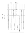
- Fig. 5 is a timing diagram illustrating the operation of a high-voltage generator circuit that includes the voltage detector block 200 of Fig. 4 .
- the high-voltage generator circuit may be similar to the high-voltage generator circuit 100 of Fig. 1 , except that the high-voltage generator circuit includes the voltage detector block 200 of Fig. 4 rather than the voltage detector block 120 of Fig. 2 .
- the control signals C1 and C2 go high and an oscillation signal OSC from an oscillation circuit (not shown) is provided to the high-voltage generator circuit.
- the control signal C2 is at a high level and a divided voltage Vdiv is lower than a reference voltage Vref (e.g., 0.8V) at an initial pump operation or before the high voltage Vpp reaches a target voltage, such that the pump control signal generator 223 generates a pump control signal PUMP_OSC in synchronization with the oscillation signal OSC. That is, when all signals applied to the NAND gate G10 of the pump control signal 223 are at a high level, the pump control signal PUMP_OSC oscillating at a given frequency is generated.
- Vref e.g. 0.8V
- a high-voltage pump block such as the high-voltage pump block 110 of Fig. 1 , operates in response to the pump control signal PUMP_OSC, and the high voltage Vpp increases to the target voltage as illustrated in Fig. 5 .
- the depletion-type MOS transistor MN10 of the voltage divider 221 delivers the voltage of the resister R10 to the node ND10 without a voltage drop.
- the comparator 222 If the high voltage Vpp reaches a target voltage, the comparator 222 generates a low-level signal. This low-level signal from the comparator 222 and an output (a high-level signal) of the inverter INV13 are inputted to the NAND gate G 10, such that the pump control signal generator 223 outputs a pump control signal PUMP_OSC of low level regardless of the state of oscillation signal OSC. Thus, the high-voltage pump block, such as the high-voltage pump block 110 of FIG. 1 , may be disabled. If the high voltage Vpp decreases by an internal operation, the voltage detector block 200 generates a pump control signal PUMP_OSC that oscillates with a given period until the high voltage Vpp increases to the target voltage. This enables the lowered high voltage Vpp to increase to the target voltage.
- each of the control signals C1 and C2 transitions from a high level to a low level.
- the control signal C1 transitions to the low level
- the NMOS transistor MN11 is turned off by the voltage divider 221.
- the control signal C2 transitions to the low level, and transistors MP13 and MN15 are turned on.
- the high voltage Vpp is discharged to a power supply voltage through the turned-on transistors MN 16, MN15 and MP13
- the node ND10 is restricted to a voltage of (VCC - Vth) (i.e., a threshold voltage of the MN10).
- the threshold voltage of the NMOS transistor MN10 has a negative value
- the node ND10 has a maximum voltage of (VCC+Vth). Therefore, the NMOS transistors MN11 and MN13, which may be low-voltage transistors, do not break down.
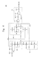
- Fig. 6 is circuit diagram illustrating another exemplary voltage detector block 600 according to the invention. Constitutent elements that perform the same function as those in Fig. 4 are marked with the same reference symbols.
- the voltage detector block 600 in Fig. 6 is identical to that of voltage detector block 200 in Fig. 4 except that the high-voltage depletion-type MOS transistor MN10 is replaced with the high-voltage enhancement-type NMOS transistor MN10'.
- the enhancement-type NMOS transistor MN10' of the voltage divider 221 is controlled by the control signal C3.
- a high-level voltage of the control signal C3 is set such that a voltage across a resistor R1 is transferred to the node ND10 without a voltage drop.
- the control signal C3 is set to a high level before the discharge operation is performed and to a low level when the discharge operation is performed. That is, when the high voltage Vpp is discharged through the discharge section 224 with the NMOS transistor MN11 being turned off, the high-voltage depletion-type NMOS transistor MN10' is turned off, and as a result the NMOS transistors MN11 and MN13 may be prevented from breaking down.
- Fig. 7 is a circuit diagram illustrating another exemplary voltage detector block 700 according to the invention.
- the voltage detector block 700 is similar to the voltage detector block 200 of FIG. 4 , with the exception that the high-voltage depletion-type MOS transistor MN10 is not used, the low-voltage NMOS transistor MN11 is replaced with the high-voltage NMOS transistor MN11', and a high-voltage NMOS transistor MN17 is added between the node ND10 and the comparator 222.
- the enhancement-type NMOS transistor MN17 of the voltage divider 221 is controlled by the control signal C3.
- the high-level voltage of the control signal C3 is set such that a voltage of the node ND10 is transferred to the NMOS transistor MN13 of the comparator 222 without a voltage drop.
- the control signal C3 is set to a high level before the discharge operation is carried out and to a low level when the discharge operation is carried out. That is, when the high voltage Vpp is discharged through the discharge section 224, the high-voltage enhancement-type NMOS transistors MN11 and MN17 are turned off. Therefore, the NMOS transistor MN13 is prevented from breaking down.
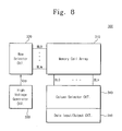
- Fig. 8 is a schematic block diagram illustrating a semiconductor memory device that includes a high-voltage generator circuit in accordance with the invention.
- the semiconductor memory device 300 includes a memory cell array 310, which includes a plurality of memory cells arranged in rows and columns. Each of the memory cells includes a volatile memory cell and a nonvolatile memory cell.
- the row selector circuit 320 selects rows (or word lines) of the memory cell array 310 in response to row address information. The selected word lines are driven with a word line voltage required for each of operation modes.
- the high-voltage generator circuit 330 generates a high voltage Vpp as a word line voltage required for each of operation modes.
- the high-voltage generator circuit 330 includes the high-voltage pump block and the voltage detector block as described above, and the voltage detector block may be one of the voltage detector blocks illustrated in Figs.
- the column selector circuit 340 selects columns (or bit lines) of the memory cell array 310 in response to column address information, and the data input/output circuit 350 writes/reads data to/from memory cells through the selected bit lines.
- Embodiments of the invention may be practiced in many ways. What follows are exemplary, non-limiting descriptions of some embodiments of the invention.
- a voltage detector circuit includes a voltage divider, a discharge section, a comparator and a control signal generator.
- the voltage divider divides a high voltage to generate a divided voltage at an output node.
- the discharge section discharges the high voltage as the power supply voltage in response to a first control signal.
- the comparator determines whether the divided voltage of the output node reaches a reference voltage.
- the control signal generator outputs a second control signal in response to the output signal of the comparator and the first control signal.
- the voltage divider includes a high-voltage prevention circuit for preventing the high voltage from being applied to a low-voltage transistor of the comparator while the high voltage is discharged.
- the voltage divider further includes a first resistor, a second resistor and a low-voltage transistor. One terminal of the first resistor is connected to the high voltage, and one terminal of the second resistor is connected to the output node.
- the low voltage transistor includes a drain connected to the other terminal of the second resistor, a source connected to a ground voltage, and a gate for receiving a third control signal.
- the high-voltage prevention circuit includes a high-voltage transistor including a drain connected to the other terminal of the first resistor, a source connected to the output node, and a gate connected to the power supply voltage.
- the high-voltage transistor is a depletion-type NMOS transistor having a negative threshold voltage.
- the high-voltage prevention circuit includes a high-voltage transistor including a drain connected to the other terminal of the first resistor, a source connected to the output node, and a gate connected to receive a fourth control signal.
- the high-voltage transistor is an enhancement-type NMOS transistor.
- the voltage divider further includes a first resistor, a second resistor, and a first and a second high-voltage transistor.
- One terminal of the first resistor is connected to the high voltage, and one terminal of the second resistor is connected to the output node.
- the first high-voltage transistor includes a drain connected to the other terminal of the second resistor, a source connected to a ground voltage, and a gate connected to receive a third control signal.
- the second high-voltage transistor includes a drain connected to the output terminal, a source connected to the comparator, and a gate connected to receive a fourth control signal.
- the third and fourth control signals are inactivated when the discharge operation is performed.
- the first and second high-voltage transistors may each be enhancement-type NMOS transistors.
- a high-voltage generator circuit includes a high-voltage pump circuit and a voltage detector circuit.
- the high-voltage pump circuit generates a high voltage in response to a pump control signal, and the voltage detector circuit generates the pump control signal according to whether the high voltage reaches a target voltage.
- the voltage detector circuit includes a voltage divider, a comparator, and a pump control signal generator.
- the voltage divider divides the high voltage and generates the divided voltage to an output node.
- the comparator determines whether the divided voltage of the output node reaches a reference voltage.
- the pump control signal generator generates the pump control signal in response to an output signal of the comparator.
- the voltage divider includes a first resistor, a high-voltage depletion-type MOS transistor, a second resistor, and a low-voltage NMOS transistor.
- One terminal of the first resistor is connected to the high voltage.
- the high-voltage depletion-type NMOS transistor includes a drain connected to the other terminal of the first resistor, a source connected to the output node, and a gate connected to the power supply voltage.
- One terminal of the second resistor is connected to the output node.
- the low-voltage NMOS transistor includes a drain connected to the other terminal of the second resistor, a source connected to a ground voltage, and a gate connected to receive a first control signal.
- the voltage detector circuit further includes a discharge section for discharging the high voltage as a power supply voltage in response to a second control signal and a complementary signal thereof.
- a high-voltage generator circuit includes a high-voltage pump circuit and a voltage detector circuit.
- the high-voltage pump circuit generates a high voltage in response to a pump control signal.
- the voltage detector circuit generates the pump control signal according to whether the high voltage reaches a target voltage.
- the high-voltage detector circuit includes a voltage divider, a comparator, and a pump control signal generator.
- the voltage divider divides a high voltage and generates the divided voltage to an output node.
- the comparator determines whether the divided voltage of the output node reaches a reference voltage.
- the pump control signal generator generates the pump control signal in response to an output signal of the comparator.
- the voltage divider includes a first resistor, a high-voltage enhancement-type MOS transistor, a second transistor, and a low voltage NMOS transistor.
- One terminal of the first resistor is connected to a high voltage.
- the high-voltage enhancement-type MOS transistor includes a drain connected to the other terminal of the first resistor, a source connected to the output node, and a gate connected to receive a first control signal.
- One terminal of the second resistor is connected to the output node.
- the low-voltage NMOS transistor includes a drain connected to the other terminal of the second resistor, a source connected to a ground voltage, and a gate connected to receive a second control signal.
- the voltage detector circuit further includes a discharge section for discharging the high voltage as a power supply voltage in response to a third control signal and a complementary signal thereof.
- the high-voltage generator circuit includes a high-voltage pump circuit and a voltage detector circuit.
- the high-voltage pump circuit generates a high voltage in response to a pump control signal.
- the voltage detector circuit generates the pump control signal according to whether the high voltage reaches a target voltage.
- the voltage detector circuit includes a voltage divider for dividing the high voltage to generate the divided voltage to an output node, a comparator for determining whether the divided voltage of the output node reaches a reference voltage, and a pump control signal generator for generating the pump control signal in response to an output signal of the comparator.
- the voltage divider includes a first resistor having one terminal connected to the high voltage and the other terminal is connected to the output node, a second resistor having a terminal connected to the output node, a first high-voltage enhancement-type NMOS transistor including a drain connected to the output node, a source connected to the comparator, and a gate connected to receive a first control signal.
- the voltage divider also includes a second high-voltage enhancement-type NMOS transistor including a drain connected to the other terminal of the second resistor, a source connected to a ground voltage, and a gate connected to receive a second control signal.
- the voltage detector circuit includes a discharge section for discharging the high voltage as a power voltage in response to a third control signal and a complementary signal thereof.
- a semiconductor memory device includes an array with memory cells arranged along row and columns, a row selector circuit for selecting at least one of the rows and driving the selected row with a word line voltage, and a high-voltage generator circuit for generating a high voltage as the word line voltage.
- the high-voltage generator includes a voltage detector circuit according to the invention.
- a low-voltage transistor may be prevented from being broken down by cutting off a high voltage directly applied to a low-voltage transistor.
Landscapes
- Engineering & Computer Science (AREA)
- Power Engineering (AREA)
- Read Only Memory (AREA)
- Dc-Dc Converters (AREA)
- Dram (AREA)
- Semiconductor Integrated Circuits (AREA)
- Semiconductor Memories (AREA)
Claims (8)
- Spannungsdetektorschaltung mit- einem Spannungsteiler (221), der dafür eingerichtet ist, eine hohe Spannung (Vpp) zu teilen, um an einem Ausgangsknoten eine geteilte Spannung (Vdiv) zu erzeugen;- einer Entladestufe (224), die dafür eingerichtet ist, die hohe Spannung in Reaktion auf ein erstes Steuersignal (C2) auf eine Versorgungsspannung zu entladen;- einem Komparator (222), der dafür eingerichtet ist, festzustellen, ob die geteilte Spannung am Ausgangsknoten eine Referenzspannung (Vref) erreicht; und- einem Steuersignalgenerator (223), der dafür eingerichtet ist, in Reaktion auf ein Komparatorausgangssignal und auf das erste Steuersignal ein zweites Steuersignal (PUMP_OSC) abzugeben;- wobei der Spannungsteiler (221) einen ersten Widerstand (R10) mit einem mit der hohen Spannung verbundenen ersten Anschluss, einen zweiten Widerstand (R12) mit einem mit dem Ausgangsknoten verbundenen ersten Anschluss und einen zweiten NMMOS-Transistor (MN11) für niedrige Spannung aufweist, der eine mit einem zweiten Anschluss des zweiten Widerstands verbundene Drain, eine mit einer Massespannung verbundene Source und ein Gate beinhaltet, das zum Empfangen eines dritten Steuersignals (C1) eingerichtet ist,dadurch gekennzeichnet, dass- der Spannungsteiler (221) eine Schutzschaltung für hohe Spannung aufweist, die dafür eingerichtet ist, zu verhindern, dass die hohe Spannung an einen ersten Transistor (MN13) für niedrige Spannung des Komparators angelegt wird, während die hohe Spannung entladen wird,- wobei die Schutzschaltung für hohe Spannung einen NMOS-Transistor (MN10) für hohe Spannung aufweist, der eine mit einem zweiten Anschluss des ersten Widerstands verbundene Drain, eine mit dem Ausgangsknoten verbundene Source und ein Gate beinhaltet, das zum Verbinden mit der Versorgungsspannung oder zum Empfangen eines vierten Steuersignals (C3) eingerichtet ist.
- Spannungsdetektorschaltung nach Anspruch 1, wobei der Transistor für hohe Spannung einen NMOS-Transistor vom Verarmungstyp mit einer negativen Schwellenspannung umfasst.
- Spannungsdetektorschaltung nach Anspruch 1, wobei das dritte und das vierte Steuersignal dafür eingerichtet sind, deaktiviert zu sein, wenn die Entladestufe die hohe Spannung auf die Versorgungsspannung entlädt, und wobei der Transistor für hohe Spannung einen NMOS-Transistor (MN10') vom Anreicherungstyp umfasst.
- Spannungsdetektorschaltung mit- einem Spannungsteiler (221), der dafür eingerichtet ist, eine hohe Spannung (Vpp) zu teilen, um an einem Ausgangsknoten eine geteilte Spannung (Vdiv) zu erzeugen;- einer Entladestufe (224), die dafür eingerichtet ist, die hohe Spannung in Reaktion auf ein erstes Steuersignal (C2) auf eine Versorgungsspannung zu entladen;- einem Komparator (222), der dafür eingerichtet ist, festzustellen, ob die geteilte Spannung am Ausgangsknoten eine Referenzspannung (Vref) erreicht; und- einem Steuersignalgenerator (223), der dafür eingerichtet ist, in Reaktion auf ein Komparatorausgangssignal und auf das erste Steuersignal ein zweites Steuersignal (PUMP_OSC) abzugeben;- wobei der Spannungsteiler (221) einen ersten Widerstand (R10) mit einem mit der hohen Spannung verbundenen ersten Anschluss, einen zweiten Widerstand (R12) mit einem mit dem Ausgangsknoten verbundenen ersten Anschluss und einen ersten NMOS-Transistor aufweist, der eine mit einem zweiten Anschluss des zweiten Widerstands verbundene Drain, eine mit einer Massespannung verbundene Source und ein Gate beinhaltet, das zum Empfangen eines dritten Steuersignals (C1) eingerichtet ist,dadurch gekennzeichnet, dass- der Spannungsteiler (221) eine Schutzschaltung für hohe Spannung aufweist, die dafür eingerichtet ist, zu verhindern, dass die hohe Spannung an einen ersten Transistor (MN13) für niedrige Spannung des Komparators angelegt wird, während die hohe Spannung entladen wird,- wobei der erste NMOS-Transistor ein NMOS-Transistor (NM11') für hohe Spannung ist und- wobei die Schutzschaltung für hohe Spannung einen zweiten NMOS-Transistor (MN17) für hohe Spannung mit einer mit einem Knoten zwischen dem ersten und dem zweiten Widerstand verbundenen Drain, einer den Ausgangsknoten, der mit dem Komparator verbunden ist, bildenden Source und einem Gate aufweist, das zum Empfangen eines vierten Steuersignals (C3) eingerichtet ist.
- Spannungsdetektorschaltung nach Anspruch 4, wobei das dritte und das vierte Steuersignal dafür eingerichtet sind, deaktiviert zu sein, wenn die Entladestufe die hohe Spannung auf die Versorgungsspannung entlädt, und wobei der erste und der zweite Transistor für hohe Spannung NMOS-Transistoren vom Anreicherungstyp beinhalten.
- Spannungsdetektorschaltung nach einem der Ansprüche 1 bis 5, wobei die Entladestufe dafür konfiguriert ist, die hohe Spannung auf die Versorgungsspannung in Reaktion auf das erste Steuersignal (C2) und ein zum ersten Steuersignal komplementäres Signal (/C2) zu entladen.
- Generatorschaltung für hohe Spannung mit- einer Pumpschaltung (110) für hohe Spannung, die zur Erzeugung einer hohen Spannung in Reaktion auf ein Pumpsteuersignal (PUMP_OSC) konfiguriert ist, und- einer Spannungsdetektorschaltung (200) nach einem der Ansprüche 1 bis 6, wobei das von der Spannungsdetektorschaltung abgegebene zweite Steuersignal das der Pumpschaltung (110) für hohe Spannung zugeführte Pumpsteuersignal (PUMP_OSC) bildet.
- Halbleiterspeicherbauelement mit- einem Feld (310) von in Zeilen und Spalten angeordneten Speicherzellen und- einer Zeilenauswahlschaltung (320) zum Auswählen wenigstens einer der Zeilen, um die ausgewählte Zeile mit einer Wortleitungsspannung zu treiben, und- einer Generatorschaltung (310) für hohe Spannung nach Anspruch 7, um eine hohe Spannung als die Wortleitungsspannung zu erzeugen.
Applications Claiming Priority (2)
| Application Number | Priority Date | Filing Date | Title |
|---|---|---|---|
| KR10-2003-0091305A KR100521385B1 (ko) | 2003-12-15 | 2003-12-15 | 고전압 발생 회로 및 그것을 포함한 반도체 메모리 장치 |
| KR2003091305 | 2003-12-15 |
Publications (3)
| Publication Number | Publication Date |
|---|---|
| EP1544991A2 EP1544991A2 (de) | 2005-06-22 |
| EP1544991A3 EP1544991A3 (de) | 2006-05-10 |
| EP1544991B1 true EP1544991B1 (de) | 2015-10-28 |
Family
ID=34511225
Family Applications (1)
| Application Number | Title | Priority Date | Filing Date |
|---|---|---|---|
| EP04027818.6A Expired - Lifetime EP1544991B1 (de) | 2003-12-15 | 2004-11-24 | Spannungsdetektionsschaltung, Hochspannungserzeugungsschaltung, und Halbleiterspeichervorrichtung |
Country Status (4)
| Country | Link |
|---|---|
| US (1) | US7154789B2 (de) |
| EP (1) | EP1544991B1 (de) |
| JP (1) | JP4520823B2 (de) |
| KR (1) | KR100521385B1 (de) |
Families Citing this family (13)
| Publication number | Priority date | Publication date | Assignee | Title |
|---|---|---|---|---|
| US20060227626A1 (en) * | 2005-04-11 | 2006-10-12 | Hynix Semiconductor Inc. | Input buffer circuit of semiconductor memory device |
| US7499345B2 (en) * | 2005-11-25 | 2009-03-03 | Giovanni Campardo | Non-volatile memory implemented with low-voltages transistors and related system and method |
| DE602006016230D1 (de) * | 2006-03-17 | 2010-09-30 | St Microelectronics Srl | Mit Niederspannungstransistoren implementierter Pegelschieber für eine Halbleiterspeichervorrichtung |
| US7432762B2 (en) * | 2006-03-30 | 2008-10-07 | Agere Systems Inc. | Circuit having enhanced input signal range |
| JP4993092B2 (ja) * | 2007-05-31 | 2012-08-08 | 富士電機株式会社 | レベルシフト回路および半導体装置 |
| KR100865852B1 (ko) * | 2007-08-08 | 2008-10-29 | 주식회사 하이닉스반도체 | 레귤레이터 및 고전압 발생기 |
| US7697349B2 (en) * | 2007-08-30 | 2010-04-13 | Macronix International Co., Ltd. | Word line boost circuit and method |
| US8284624B2 (en) | 2009-02-03 | 2012-10-09 | Samsung Electronics Co., Ltd. | Level detector, internal voltage generator including level detector, and semiconductor memory device including internal voltage generator |
| CN104407194B (zh) * | 2014-08-27 | 2017-04-19 | 北京中电华大电子设计有限责任公司 | 一种电压检测点离散程度和速度可调的电压传感器装置 |
| JP6591220B2 (ja) * | 2015-07-15 | 2019-10-16 | ルネサスエレクトロニクス株式会社 | 半導体装置および電力制御装置 |
| US11437117B2 (en) | 2020-05-29 | 2022-09-06 | Micron Technology, Inc. | NAND flash array defect real time detection |
| US11482298B2 (en) * | 2020-05-29 | 2022-10-25 | Micron Technology, Inc. | Device field degradation and factory defect detection by pump clock monitoring |
| KR102905853B1 (ko) | 2021-10-15 | 2025-12-31 | 삼성전자주식회사 | 스토리지 장치 및 전자 장치 |
Citations (1)
| Publication number | Priority date | Publication date | Assignee | Title |
|---|---|---|---|---|
| EP0701259A2 (de) * | 1994-09-09 | 1996-03-13 | Samsung Electronics Co., Ltd. | Selbst-Programmierschaltung für eine nicht-flüchtige Speicheranordnung |
Family Cites Families (13)
| Publication number | Priority date | Publication date | Assignee | Title |
|---|---|---|---|---|
| KR920006991A (ko) * | 1990-09-25 | 1992-04-28 | 김광호 | 반도체메모리 장치의 고전압발생회로 |
| US5329168A (en) * | 1991-12-27 | 1994-07-12 | Nec Corporation | Semiconductor integrated circuit device equipped with substrate biasing system selectively powered from internal and external power sources |
| FR2694448B1 (fr) * | 1992-07-31 | 1994-10-07 | Sgs Thomson Microelectronics | Dispositif de protection d'un circuit intégré contre les coupures d'alimentation. |
| JPH09260594A (ja) * | 1996-03-22 | 1997-10-03 | Toshiba Corp | 半導体集積回路装置 |
| JPH09288897A (ja) | 1996-04-19 | 1997-11-04 | Sony Corp | 電圧供給回路 |
| US5835420A (en) * | 1997-06-27 | 1998-11-10 | Aplus Flash Technology, Inc. | Node-precise voltage regulation for a MOS memory system |
| JP3773718B2 (ja) * | 1999-09-20 | 2006-05-10 | 株式会社東芝 | 半導体集積回路 |
| IT1316271B1 (it) * | 2000-12-28 | 2003-04-03 | Micron Technology Inc | Generatore di impulsi compensato in tensione e temperatura. |
| KR100500623B1 (ko) * | 2001-03-05 | 2005-07-12 | 가부시끼가이샤 도시바 | 강유전체 메모리 |
| US6690148B2 (en) | 2001-11-28 | 2004-02-10 | Micron Technology, Inc. | Method and circuit for limiting a pumped voltage |
| KR100420125B1 (ko) * | 2002-02-02 | 2004-03-02 | 삼성전자주식회사 | 비휘발성 반도체 메모리 장치와 그것의 파워-업 독출 방법 |
| KR100460459B1 (ko) * | 2002-07-30 | 2004-12-08 | 삼성전자주식회사 | 향상된 테스트 모드를 갖는 반도체 메모리 장치 |
| US6967877B2 (en) * | 2003-09-09 | 2005-11-22 | Taiwan Semiconductor Manufacturing Co., Ltd. | Temperature detecting circuit for controlling a self-refresh period of a semiconductor memory device |
-
2003
- 2003-12-15 KR KR10-2003-0091305A patent/KR100521385B1/ko not_active Expired - Fee Related
-
2004
- 2004-10-28 US US10/977,426 patent/US7154789B2/en not_active Expired - Lifetime
- 2004-11-05 JP JP2004322825A patent/JP4520823B2/ja not_active Expired - Fee Related
- 2004-11-24 EP EP04027818.6A patent/EP1544991B1/de not_active Expired - Lifetime
Patent Citations (1)
| Publication number | Priority date | Publication date | Assignee | Title |
|---|---|---|---|---|
| EP0701259A2 (de) * | 1994-09-09 | 1996-03-13 | Samsung Electronics Co., Ltd. | Selbst-Programmierschaltung für eine nicht-flüchtige Speicheranordnung |
Also Published As
| Publication number | Publication date |
|---|---|
| JP4520823B2 (ja) | 2010-08-11 |
| US20050128821A1 (en) | 2005-06-16 |
| EP1544991A2 (de) | 2005-06-22 |
| JP2005185088A (ja) | 2005-07-07 |
| KR100521385B1 (ko) | 2005-10-12 |
| KR20050059608A (ko) | 2005-06-21 |
| EP1544991A3 (de) | 2006-05-10 |
| US7154789B2 (en) | 2006-12-26 |
Similar Documents
| Publication | Publication Date | Title |
|---|---|---|
| KR100299254B1 (ko) | 플래시메모리용전압공급기 | |
| KR100317647B1 (ko) | 포지티브파워서플라이 | |
| EP1544991B1 (de) | Spannungsdetektionsschaltung, Hochspannungserzeugungsschaltung, und Halbleiterspeichervorrichtung | |
| US7372739B2 (en) | High voltage generation and regulation circuit in a memory device | |
| CA2185333C (en) | Method and apparatus for providing an ultra low power regulated negative charge pump | |
| KR970706580A (ko) | 고속 저전압 비휘발성 메모리(high speed, low voltage non-volatile memory) | |
| US6111789A (en) | Nonvolatile semiconductor memory device | |
| KR20190103008A (ko) | 레벨 시프터 및 반도체 장치 | |
| KR20000075834A (ko) | 고전압 발생기를 갖춘 플래시 메모리를 위한 고전압 nmos통과 게이트 | |
| EP1892600B1 (de) | Spannungsregler für nichtflüchtige speichereinheiten mit niedrigspannungstransistoren | |
| KR100764740B1 (ko) | 플래시 메모리 장치 및 그것을 위한 고전압 발생회로 | |
| US6072358A (en) | High voltage pump circuit with reduced oxide stress | |
| KR100587683B1 (ko) | 불휘발성 반도체 메모리 장치에서의 고전압 발생회로 | |
| US5696461A (en) | Power-on reset circuit | |
| US6288594B1 (en) | Monolithically integrated selector for electrically programmable memory cell devices | |
| KR20200144495A (ko) | 전압 발생 회로, 반도체 스토리지 디바이스 및 그 비트 라인 충전 방법 | |
| US6480040B2 (en) | Device for the detection of a high voltage greater than a supply voltage | |
| KR100684911B1 (ko) | 반도체 메모리 장치의 전압 레귤레이터 회로 | |
| US5978268A (en) | Circuit for the generation of voltage for the programming or erasure of a memory that uses floating-gate transistors | |
| KR100633598B1 (ko) | 하프 전원 전압 발생 회로 | |
| JPH09503880A (ja) | 改良型電源電圧検出回路 | |
| KR960009954B1 (ko) | 퓨즈를 이용한 고전압 발생회로 | |
| KR100461976B1 (ko) | 파워온 리세트회로 | |
| CN112929015A (zh) | 开关电路 | |
| US20070091683A1 (en) | Method for erasing programmable interconnect cells for field programmable gate arrays using reverse bias voltage |
Legal Events
| Date | Code | Title | Description |
|---|---|---|---|
| PUAI | Public reference made under article 153(3) epc to a published international application that has entered the european phase |
Free format text: ORIGINAL CODE: 0009012 |
|
| AK | Designated contracting states |
Kind code of ref document: A2 Designated state(s): AT BE BG CH CY CZ DE DK EE ES FI FR GB GR HU IE IS IT LI LU MC NL PL PT RO SE SI SK TR |
|
| AX | Request for extension of the european patent |
Extension state: AL HR LT LV MK YU |
|
| RIN1 | Information on inventor provided before grant (corrected) |
Inventor name: BYEON, DAE-SEOK Inventor name: KIM, JONG-HWA |
|
| PUAL | Search report despatched |
Free format text: ORIGINAL CODE: 0009013 |
|
| AK | Designated contracting states |
Kind code of ref document: A3 Designated state(s): AT BE BG CH CY CZ DE DK EE ES FI FR GB GR HU IE IS IT LI LU MC NL PL PT RO SE SI SK TR |
|
| AX | Request for extension of the european patent |
Extension state: AL HR LT LV MK YU |
|
| 17P | Request for examination filed |
Effective date: 20060912 |
|
| AKX | Designation fees paid |
Designated state(s): DE FR GB |
|
| 17Q | First examination report despatched |
Effective date: 20110831 |
|
| RAP1 | Party data changed (applicant data changed or rights of an application transferred) |
Owner name: SAMSUNG ELECTRONICS CO., LTD. |
|
| RIC1 | Information provided on ipc code assigned before grant |
Ipc: H02M 3/07 20060101AFI20150416BHEP Ipc: H02M 1/00 20070101ALN20150416BHEP |
|
| GRAP | Despatch of communication of intention to grant a patent |
Free format text: ORIGINAL CODE: EPIDOSNIGR1 |
|
| RIC1 | Information provided on ipc code assigned before grant |
Ipc: H02M 3/07 20060101AFI20150430BHEP Ipc: H02M 1/00 20070101ALN20150430BHEP |
|
| INTG | Intention to grant announced |
Effective date: 20150527 |
|
| GRAS | Grant fee paid |
Free format text: ORIGINAL CODE: EPIDOSNIGR3 |
|
| GRAA | (expected) grant |
Free format text: ORIGINAL CODE: 0009210 |
|
| AK | Designated contracting states |
Kind code of ref document: B1 Designated state(s): DE FR GB |
|
| REG | Reference to a national code |
Ref country code: GB Ref legal event code: FG4D |
|
| REG | Reference to a national code |
Ref country code: DE Ref legal event code: R096 Ref document number: 602004048133 Country of ref document: DE |
|
| REG | Reference to a national code |
Ref country code: FR Ref legal event code: PLFP Year of fee payment: 12 |
|
| REG | Reference to a national code |
Ref country code: DE Ref legal event code: R097 Ref document number: 602004048133 Country of ref document: DE |
|
| PLBE | No opposition filed within time limit |
Free format text: ORIGINAL CODE: 0009261 |
|
| STAA | Information on the status of an ep patent application or granted ep patent |
Free format text: STATUS: NO OPPOSITION FILED WITHIN TIME LIMIT |
|
| 26N | No opposition filed |
Effective date: 20160729 |
|
| REG | Reference to a national code |
Ref country code: FR Ref legal event code: PLFP Year of fee payment: 13 |
|
| REG | Reference to a national code |
Ref country code: FR Ref legal event code: PLFP Year of fee payment: 14 |
|
| REG | Reference to a national code |
Ref country code: FR Ref legal event code: PLFP Year of fee payment: 15 |
|
| P01 | Opt-out of the competence of the unified patent court (upc) registered |
Effective date: 20230520 |
|
| PGFP | Annual fee paid to national office [announced via postgrant information from national office to epo] |
Ref country code: FR Payment date: 20230929 Year of fee payment: 20 |
|
| PGFP | Annual fee paid to national office [announced via postgrant information from national office to epo] |
Ref country code: GB Payment date: 20231006 Year of fee payment: 20 |
|
| PGFP | Annual fee paid to national office [announced via postgrant information from national office to epo] |
Ref country code: DE Payment date: 20230926 Year of fee payment: 20 |
|
| REG | Reference to a national code |
Ref country code: DE Ref legal event code: R071 Ref document number: 602004048133 Country of ref document: DE |
|
| REG | Reference to a national code |
Ref country code: GB Ref legal event code: PE20 Expiry date: 20241123 |
|
| PG25 | Lapsed in a contracting state [announced via postgrant information from national office to epo] |
Ref country code: GB Free format text: LAPSE BECAUSE OF EXPIRATION OF PROTECTION Effective date: 20241123 |
|
| PG25 | Lapsed in a contracting state [announced via postgrant information from national office to epo] |
Ref country code: GB Free format text: LAPSE BECAUSE OF EXPIRATION OF PROTECTION Effective date: 20241123 |