EP1544907B1 - Dispositif de transistors avec canal de type p en matériau delafossite - Google Patents
Dispositif de transistors avec canal de type p en matériau delafossite Download PDFInfo
- Publication number
- EP1544907B1 EP1544907B1 EP04257620.7A EP04257620A EP1544907B1 EP 1544907 B1 EP1544907 B1 EP 1544907B1 EP 04257620 A EP04257620 A EP 04257620A EP 1544907 B1 EP1544907 B1 EP 1544907B1
- Authority
- EP
- European Patent Office
- Prior art keywords
- channel
- gate
- type
- transparent
- contacts
- Prior art date
- Legal status (The legal status is an assumption and is not a legal conclusion. Google has not performed a legal analysis and makes no representation as to the accuracy of the status listed.)
- Expired - Lifetime
Links
Images


Classifications
-
- H—ELECTRICITY
- H10—SEMICONDUCTOR DEVICES; ELECTRIC SOLID-STATE DEVICES NOT OTHERWISE PROVIDED FOR
- H10D—INORGANIC ELECTRIC SEMICONDUCTOR DEVICES
- H10D30/00—Field-effect transistors [FET]
- H10D30/60—Insulated-gate field-effect transistors [IGFET]
- H10D30/67—Thin-film transistors [TFT]
- H10D30/674—Thin-film transistors [TFT] characterised by the active materials
- H10D30/6755—Oxide semiconductors, e.g. zinc oxide, copper aluminium oxide or cadmium stannate
-
- H—ELECTRICITY
- H10—SEMICONDUCTOR DEVICES; ELECTRIC SOLID-STATE DEVICES NOT OTHERWISE PROVIDED FOR
- H10D—INORGANIC ELECTRIC SEMICONDUCTOR DEVICES
- H10D30/00—Field-effect transistors [FET]
- H10D30/01—Manufacture or treatment
- H10D30/021—Manufacture or treatment of FETs having insulated gates [IGFET]
- H10D30/031—Manufacture or treatment of FETs having insulated gates [IGFET] of thin-film transistors [TFT]
-
- H—ELECTRICITY
- H10—SEMICONDUCTOR DEVICES; ELECTRIC SOLID-STATE DEVICES NOT OTHERWISE PROVIDED FOR
- H10D—INORGANIC ELECTRIC SEMICONDUCTOR DEVICES
- H10D30/00—Field-effect transistors [FET]
- H10D30/60—Insulated-gate field-effect transistors [IGFET]
- H10D30/67—Thin-film transistors [TFT]
- H10D30/6729—Thin-film transistors [TFT] characterised by the electrodes
- H10D30/673—Thin-film transistors [TFT] characterised by the electrodes characterised by the shapes, relative sizes or dispositions of the gate electrodes
- H10D30/6733—Multi-gate TFTs
- H10D30/6734—Multi-gate TFTs having gate electrodes arranged on both top and bottom sides of the channel, e.g. dual-gate TFTs
-
- H—ELECTRICITY
- H10—SEMICONDUCTOR DEVICES; ELECTRIC SOLID-STATE DEVICES NOT OTHERWISE PROVIDED FOR
- H10D—INORGANIC ELECTRIC SEMICONDUCTOR DEVICES
- H10D86/00—Integrated devices formed in or on insulating or conducting substrates, e.g. formed in silicon-on-insulator [SOI] substrates or on stainless steel or glass substrates
- H10D86/40—Integrated devices formed in or on insulating or conducting substrates, e.g. formed in silicon-on-insulator [SOI] substrates or on stainless steel or glass substrates characterised by multiple TFTs
- H10D86/421—Integrated devices formed in or on insulating or conducting substrates, e.g. formed in silicon-on-insulator [SOI] substrates or on stainless steel or glass substrates characterised by multiple TFTs having a particular composition, shape or crystalline structure of the active layer
- H10D86/423—Integrated devices formed in or on insulating or conducting substrates, e.g. formed in silicon-on-insulator [SOI] substrates or on stainless steel or glass substrates characterised by multiple TFTs having a particular composition, shape or crystalline structure of the active layer comprising semiconductor materials not belonging to the Group IV, e.g. InGaZnO
-
- H—ELECTRICITY
- H10—SEMICONDUCTOR DEVICES; ELECTRIC SOLID-STATE DEVICES NOT OTHERWISE PROVIDED FOR
- H10D—INORGANIC ELECTRIC SEMICONDUCTOR DEVICES
- H10D86/00—Integrated devices formed in or on insulating or conducting substrates, e.g. formed in silicon-on-insulator [SOI] substrates or on stainless steel or glass substrates
- H10D86/40—Integrated devices formed in or on insulating or conducting substrates, e.g. formed in silicon-on-insulator [SOI] substrates or on stainless steel or glass substrates characterised by multiple TFTs
- H10D86/60—Integrated devices formed in or on insulating or conducting substrates, e.g. formed in silicon-on-insulator [SOI] substrates or on stainless steel or glass substrates characterised by multiple TFTs wherein the TFTs are in active matrices
-
- H—ELECTRICITY
- H10—SEMICONDUCTOR DEVICES; ELECTRIC SOLID-STATE DEVICES NOT OTHERWISE PROVIDED FOR
- H10D—INORGANIC ELECTRIC SEMICONDUCTOR DEVICES
- H10D99/00—Subject matter not provided for in other groups of this subclass
Definitions
- Thin film transistors are of great interest in the semiconductor industry as they represent a more universally applicable technology than traditional transistor devices. In some cases, thin film transistors also provide new properties that designers may leverage for great advantage. One interesting property is transparency.
- PATENT ABSTRACT FROM JAPAN vol. 2000, no. 11 & JP 2000 228516 disclose a laminated thin film that has a structure in which an inorganic material layer contains oxide containing monovalent Cu.
- OTABE TAKUYA ET AL "n-type electrical conduction in transparent thin films of delafossite-type Agln02 " disclose thin films of AgInO2 prepared to find transparent and n-type conducting oxide with a delafossite structure.
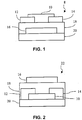
- FIG. 1 shows an exemplary bottom gate thin-film transistor 8 useful in explaining the present invention.
- a p-type transparent channel 10 is controlled by co-planar source and drain contacts 12, 14 and a gate contact 16, which is isolated from the transparent channel 10 by gate dielectric 18.
- a substrate 20 upon which the transistor 8 is formed should have good dielectric properties and be compatible with the thin film materials used to form the transistor 8.
- Suitable exemplary substrates include glass and plastic. Particular examples include polycarbonate, polyarylate, polyethylenterephtalate (PET), polyestersulfone (PES), polyimide, polyolefin, and polyethylene naphtthalate (PEN).
- Examples of the transistor 8 include partially transparent devices, e.g., where the p-type transparent channel 10 is the only transparent thin film, as well as completely transparent devices, i.e., where all of the thin films are formed from transparent materials. Additional embodiments include the use of a transparent substrate.
- the p-type transparent channel 10 is a delafossite film that is undoped or lightly doped. In lightly doped layers, the delafossite has a doping level low enough to maintain its transparency and semiconductor performance.
- lightly doped embodiments of the invention include doping levels that result in a carrier (hole) concentration of less than ⁇ 10 17 cm -3 .
- the apparent optical band gap of undoped delafossites is in the near-UV range, while heavily doped (and conductive) films may be nearly opaque.
- Delafossites are the materials having the crystal structure of CuFeO 2 .
- Example delafossites include CuScO 2 , CuAlO 2 , CuYO 2 , CuFeO 2 , CuCrO 2 , CuGaO 2 , CuInO 2 , AgCoO 2 , AgGaO 2 , AgInO 2 , AgScO 2 , and AgCrO 2 .
- Any dopant suitable to provide hole carriers may be used.
- CuYO 2 and CuInO 2 can be doped p-type using Ca.
- CuCrO 2 can be doped p-type using Mg. Also, processing that results in a slight surplus of oxygen is often used to obtain p-type conductivity in these materials, and if controlled properly, may produce light doping levels for use as a p-type semiconductor channel in a transistor. Lightly doped p-type channels will yield an enhancement-mode or weakly depletion-mode transistor device. A negative gate voltage will draw holes from the source and drain contacts 12, 14 to the p-type channel 10 in a region near its interface with the gate dielectric 18. Lightly doped delafossite films additionally have the advantage of providing a reasonably- ⁇ small positive gate voltage to deplete holes from the channel, thereby producing a relatively low gate voltage turn-off condition.
- the gate dielectric 18 for example may be a film of SiO 2 , Si 3 N 4 , Al 2 O 3 , Ta 2 O 5 , HfO 2 , ZrO 2 , or the like.
- the gate contact 16 and source/drain layers may, for example, be formed from a transparent conductor (i.e., a p-type doped wide-band gap semiconductor) such as p-type doped GaN, BaCu 2 S 2 , NiO, Cu 2 O, or various delafossites (CuScO 2 , CuAlO 2 , CuYO 2 , CuFeO 2 , CuCrO 2 , CuGaO 2 , CuInO 2 , AgCoO 2 , AgGaO 2 , AgInO 2 , AgScO 2 , AgCrO 2 ), or the like.
- Gate contact and source/drain layers may also comprise metals such as Au, Pt, Pd, Ni, Cu, W, Mo, Cr, Ag, In, Sn, Ga, Zn, Al, Ti, or the like.
- a source and drain contact material may be selected for a desired level of electrical performance. Overall device performance is likely to vary significantly for devices built using various source/drain contact materials. If the source, drain and gate contact films are formed of transparent materials, appropriate gate materials will likely also be transparent, thereby producing a complete device that is substantially transparent.
- the delafossite channel 10 and transistor 8 have the capability to provide hole injection in the lightly doped channel, thereby creating a p-type device.
- Other transparent semiconductors typically have a high ionization potential (separation between valence band edge and vacuum level), e.g. in the range of 6-8 eV.
- Hole injection into the transparent channel is achieved when the source and drain contacts are formed of a material (metal or doped semiconductor) having a work function that is nearly equal to or greater than the ionization potential of the channel material.
- high work function metals e.g., Au, Pd and Pt, have work functions smaller than 6eV.
- the lower ionization potential of the lightly doped delafossite materials provides the ability to meet the conditions for hole injection.
- FIGs. 2-6 Other exemplary transistors useful in explaining the present invention are shown in FIGs. 2-6 .
- the reference numerals from FIG. 1 are adopted to label similar elements in FIGs. 2-6 .
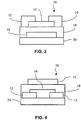
- FIG. 2 shows an exemplary top gate p-type transparent channel thin film transistor 22 with co-planar source and drain contacts 12 and 14.
- FIG. 3 shows an exemplary bottom gate p-type transparent channel thin film transistor 24 with staggered contacts.
- FIG. 4 shows an exemplary top gate p-type transparent channel thin film transistor 26 with staggered contacts.
- FIG. 5 illustrates an exemplary dual gate p-type transparent channel thin film transistor 28.
- FIG. 6 illustrates another exemplary dual gate p-type transparent channel thin film transistor 30.
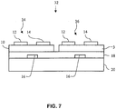
- FIG. 7 shows a portion of an exemplary embodiment CMOS circuit 32 including a p-type transparent thin film transistor 34 and an n-type transparent thin film transistor 36.
- the p-type transparent thin film transistor 34 includes a lightly doped transparent thin film channel 10.
- the n-type transparent thin film transistor 36 includes an n-type transparent thin film channel 38, for example ZnO.
- Alternative embodiments include CMOS integrations that include non-transparent thin film transistors, both n-type and p*type. Source 12, drain 14 and gate 16 contacts form part of a circuit interconnect pattern in the CMOS circuit 32. While two transistors are shown, the circuit 32 may include many transistors.
- the circuit may be arranged, for example, as an integrated circuit where transistors 34 and 36, and other transistors in the integrated circuit act as switches.
- the circuit arrangement and applied voltages may provide amplification, for example.
- the circuit arrangement and applied voltages may also provide operation as a load device, for example to provide a resistance in a CMOS circuit.
- the lightly doped delafossite channel 10 uses a negative voltage to draw holes from the source 12 and drain 14 into the channel near the gate insulator.
- a range of negative voltages for a CMOS integrated circuit arranged in a CMOS switch configuration produces a conducting operation in the switch. As mentioned above, reasonable positive gate voltages will deplete the channel of free holes to turn off the transistor.
- Thin-film deposition techniques such as evaporation (thermal, e-beam), sputtering (DC, RF, ion beam), chemical vapor deposition (CVD), atomic layer deposition (ALD), molecular beam epitaxy (MBE), and the like may be employed. Alternate methods may also be employed, such as solution-based deposition from a liquid precursor (spin-coating, inkjet printing, etc). Film patterning may employ traditional photolithography combined with etching or lift-off processes, or may use alternate techniques such as shadow masking or direct-write patterning (i.e., inkjet printing).
- an initial deposition on the substrate 20 is an inkjet printing of a solution-based conductor to form the gate contact 16.
- the gate contact 16 may be part of a circuit interconnect pattern, for example patterned by a direct write process.
- a spin coating is used to deposit gate contact material, which is then patterned by a photolithography and etching procedure, or perhaps a more sophisticated process such as laser ablation.
- a spin coating process for example, then deposits gate dielectric material 18. Additional direct write steps form the channel 10, and the gate and source contacts.
- FIG. 8 shows an exemplary embodiment including a CMOS circuit 32 in accordance with FIG. 7 combined with an integrated device 40.
- the entire CMOS thin film circuit 32 is formed to be transparent, i.e., p-type thin film transistors 34 and n-type thin film transistors 36 are formed as transparent devices.
- the substrate 20 is also transparent, e.g., a transparent plastic.
- the integrated device 40 may be, for example, an emissive display or include receptors for sensing or encoding or some other function.
- the integrated device 40 may be in the form of a thick film integration, e.g., silicon wafer based integration or a group III-V based integration, bonded or otherwise attached to the substrate 20.
- CMOS circuit is transparent, one optical path that may be defined to the integrated device 40 is through the CMOS circuit 32. This provides designers with an added level of flexibility, as electronics embodied in the CMOS thin film circuit 32 may be placed irrespective of optical paths necessary for device operation. In other embodiments of a display or sensor, the CMOS thin film circuit 32 is outside of the optical paths in an integrated device. A fully transparent CMOS thin film circuit 32 or a CMOS circuit 32 with transparent channels is less likely to be affected by light in a display or sensor device.
Landscapes
- Thin Film Transistor (AREA)
- Electrodes Of Semiconductors (AREA)
Claims (4)
- Dispositif de transistor comprenant un circuit CMOS (32), comportant :un matériau de délafossite sensiblement transparent dopé de canal de type p (10), dans lequel le matériau est dopé pour donner une concentration de porteurs inférieure à environ 1017 cm-3, le matériau du canal ayant un potentiel d'ionisation ;un premier contact de source (12) interfacé avec ledit canal de type p (10) ;un premier contact de drain (14) interfacé avec ledit canal de type p (10) ;un canal de type n (38) ;un second contact de source (12) interfacé avec ledit canal de type n (38) ;un second contact de drain (14) interfacé avec ledit canal de type n (38) ; etun diélectrique de grille (18) entre un premier et un second contacts de grille (16), le canal de type p (10) et le canal de type n (10), dans lequel :le premier contact de grille (16) est formé sur un substrat (20), ledit diélectrique de grille (18) est formé sur lesdits contacts de grille (16) et ledit canal (10) est formé sur ledit diélectrique de grille (18) ;les contacts de grille, de source et de drain (16, 12, 14) sont agencés pour former un motif d'interconnexion de circuit ; etles contacts de source à canal et de drain à canal ayant une fonction de travail presque égale ou supérieure au potentiel d'ionisation du matériau de canal, dans lequel les premiers contacts (12, 14, 16) forment le transistor à couche mince de type p (34) ; et dans lequel les seconds contacts forment un transistor à canal transparent de type n (36) connecté à travers le motif de circuit pour former le circuit CMOS (32).
- Dispositif selon la revendication 1, dans lequel le matériau de délafossite est choisi dans le groupe de CuScO2, CuAlO2, CuYO2, CuFeO2, CuCrO2, CuGaO2, CuInO2, AgCoO2, AgGaO2, AgInO2, AgScO2 et AgCrO2.
- Dispositif selon la revendication 2, dans lequel lesdits contacts de source, de drain et de grille (12, 14, 16) comprennent un semi-conducteur dopé choisi dans le groupe constitué par GaN, BaCu2S2, NiO, Cu2O, CuScO2, CuAlO2, CuYO2, CuFeO2, CuCrO2, CuGaO2, CulnO2 ; AgCoO2, AgGaO2, AgInO2, AgScO2, AgCrO2.
- Dispositif selon l'une quelconque des revendications précédentes, dans lequel chacun desdits contacts de source, de drain et de grille (12, 14, 16) et ledit diélectrique de grille (18) est formé d'un matériau transparent de sorte que le dispositif (8) comprend un dispositif transparent.
Applications Claiming Priority (2)
| Application Number | Priority Date | Filing Date | Title |
|---|---|---|---|
| US738690 | 2003-12-17 | ||
| US10/738,690 US7026713B2 (en) | 2003-12-17 | 2003-12-17 | Transistor device having a delafossite material |
Publications (2)
| Publication Number | Publication Date |
|---|---|
| EP1544907A1 EP1544907A1 (fr) | 2005-06-22 |
| EP1544907B1 true EP1544907B1 (fr) | 2020-02-12 |
Family
ID=34523178
Family Applications (1)
| Application Number | Title | Priority Date | Filing Date |
|---|---|---|---|
| EP04257620.7A Expired - Lifetime EP1544907B1 (fr) | 2003-12-17 | 2004-12-08 | Dispositif de transistors avec canal de type p en matériau delafossite |
Country Status (6)
| Country | Link |
|---|---|
| US (2) | US7026713B2 (fr) |
| EP (1) | EP1544907B1 (fr) |
| JP (1) | JP2005183984A (fr) |
| KR (1) | KR101120151B1 (fr) |
| CN (1) | CN100483741C (fr) |
| TW (1) | TWI335079B (fr) |
Families Citing this family (43)
| Publication number | Priority date | Publication date | Assignee | Title |
|---|---|---|---|---|
| EP1737044B1 (fr) | 2004-03-12 | 2014-12-10 | Japan Science and Technology Agency | Oxyde amorphe et transistor film mince |
| US9953259B2 (en) | 2004-10-08 | 2018-04-24 | Thin Film Electronics, Asa | RF and/or RF identification tag/device having an integrated interposer, and methods for making and using the same |
| US8058652B2 (en) * | 2004-10-28 | 2011-11-15 | Semiconductor Energy Laboratory Co., Ltd. | Semiconductor device used as electro-optical device having channel formation region containing first element, and source or drain region containing second element |
| EP1998373A3 (fr) | 2005-09-29 | 2012-10-31 | Semiconductor Energy Laboratory Co, Ltd. | Dispositif de semi-conducteur disposant d'une couche de semi-conducteur d'oxyde et son procédé de fabrication |
| JP2007149746A (ja) * | 2005-11-24 | 2007-06-14 | National Institute Of Advanced Industrial & Technology | 透明酸化物半導体接合 |
| US7314801B2 (en) * | 2005-12-20 | 2008-01-01 | Palo Alto Research Center Incorporated | Semiconductor device having a surface conducting channel and method of forming |
| CN100408166C (zh) * | 2006-01-13 | 2008-08-06 | 南京大学 | AgTO2型复合氧化物可见光响应光催化材料及其应用 |
| US20070261951A1 (en) * | 2006-04-06 | 2007-11-15 | Yan Ye | Reactive sputtering zinc oxide transparent conductive oxides onto large area substrates |
| JP5164357B2 (ja) * | 2006-09-27 | 2013-03-21 | キヤノン株式会社 | 半導体装置及び半導体装置の製造方法 |
| US7927713B2 (en) * | 2007-04-27 | 2011-04-19 | Applied Materials, Inc. | Thin film semiconductor material produced through reactive sputtering of zinc target using nitrogen gases |
| WO2009018509A1 (fr) * | 2007-08-02 | 2009-02-05 | Applied Materials, Inc. | Transistors à film mince utilisant des matériaux semi-conducteurs à film mince |
| JP2009048371A (ja) * | 2007-08-17 | 2009-03-05 | Kovio Inc | 集積化インタポーザを有するrfタグ/装置及/又はびrfidタグ/装置、並びにその製造方法及び使用方法 |
| CN101779290B (zh) * | 2007-09-25 | 2013-02-27 | 第一太阳能有限公司 | 包括界面层的光伏器件 |
| US8980066B2 (en) * | 2008-03-14 | 2015-03-17 | Applied Materials, Inc. | Thin film metal oxynitride semiconductors |
| WO2009117438A2 (fr) * | 2008-03-20 | 2009-09-24 | Applied Materials, Inc. | Procédé de fabrication de réseau de transistors à couches minces d’oxyde métalliques avec couche d’arrêt de gravure |
| US7879698B2 (en) * | 2008-03-24 | 2011-02-01 | Applied Materials, Inc. | Integrated process system and process sequence for production of thin film transistor arrays using doped or compounded metal oxide semiconductor |
| US8258511B2 (en) * | 2008-07-02 | 2012-09-04 | Applied Materials, Inc. | Thin film transistors using multiple active channel layers |
| TWI770659B (zh) | 2008-07-31 | 2022-07-11 | 日商半導體能源研究所股份有限公司 | 半導體裝置及半導體裝置的製造方法 |
| KR101259727B1 (ko) | 2008-10-24 | 2013-04-30 | 가부시키가이샤 한도오따이 에네루기 켄큐쇼 | 반도체 장치 |
| US8106400B2 (en) | 2008-10-24 | 2012-01-31 | Semiconductor Energy Laboratory Co., Ltd. | Semiconductor device and method for manufacturing the same |
| TWI431130B (zh) * | 2008-12-19 | 2014-03-21 | Applied Materials Inc | 銅黑銅鐵礦透明p型半導體之製造及應用方法 |
| KR101476817B1 (ko) * | 2009-07-03 | 2014-12-26 | 가부시키가이샤 한도오따이 에네루기 켄큐쇼 | 트랜지스터를 갖는 표시 장치 및 그 제작 방법 |
| KR101733718B1 (ko) | 2009-09-24 | 2017-05-10 | 어플라이드 머티어리얼스, 인코포레이티드 | 소스 및 드레인 금속 식각을 위해 습식 프로세스를 이용하여 금속 산화물 또는 금속 산질화물 tft들을 제조하는 방법들 |
| US8840763B2 (en) * | 2009-09-28 | 2014-09-23 | Applied Materials, Inc. | Methods for stable process in a reactive sputtering process using zinc or doped zinc target |
| KR20250075719A (ko) * | 2009-10-30 | 2025-05-28 | 가부시키가이샤 한도오따이 에네루기 켄큐쇼 | 반도체 장치 |
| CN102656683B (zh) | 2009-12-11 | 2015-02-11 | 株式会社半导体能源研究所 | 半导体装置 |
| KR20110069454A (ko) * | 2009-12-17 | 2011-06-23 | 한국전자통신연구원 | 박막 트랜지스터 및 그 형성방법 |
| CN105590646B (zh) * | 2009-12-25 | 2019-01-08 | 株式会社半导体能源研究所 | 存储器装置、半导体器件和电子装置 |
| US8759917B2 (en) * | 2010-01-04 | 2014-06-24 | Samsung Electronics Co., Ltd. | Thin-film transistor having etch stop multi-layer and method of manufacturing the same |
| KR101399609B1 (ko) | 2010-02-05 | 2014-05-27 | 가부시키가이샤 한도오따이 에네루기 켄큐쇼 | 반도체 장치, 및 반도체 장치의 제조 방법 |
| CN102939659B (zh) * | 2010-06-11 | 2016-08-17 | 株式会社半导体能源研究所 | 半导体器件及半导体器件的制造方法 |
| US20120001179A1 (en) * | 2010-07-02 | 2012-01-05 | Semiconductor Energy Laboratory Co., Ltd. | Semiconductor device |
| JP2012216780A (ja) * | 2011-03-31 | 2012-11-08 | Ricoh Co Ltd | p型酸化物、p型酸化物製造用組成物、p型酸化物の製造方法、半導体素子、表示素子、画像表示装置、及びシステム |
| JP5783094B2 (ja) | 2011-11-30 | 2015-09-24 | 株式会社リコー | p型酸化物、p型酸化物製造用組成物、p型酸化物の製造方法、半導体素子、表示素子、画像表示装置、及びシステム |
| JP6547273B2 (ja) | 2013-12-26 | 2019-07-24 | 株式会社リコー | p型酸化物半導体、p型酸化物半導体製造用組成物、p型酸化物半導体の製造方法、半導体素子、表示素子、画像表示装置、及びシステム |
| US9985139B2 (en) * | 2014-11-12 | 2018-05-29 | Qualcomm Incorporated | Hydrogenated p-channel metal oxide semiconductor thin film transistors |
| US9685542B2 (en) | 2014-12-30 | 2017-06-20 | Qualcomm Incorporated | Atomic layer deposition of P-type oxide semiconductor thin films |
| US9647135B2 (en) | 2015-01-22 | 2017-05-09 | Snaptrack, Inc. | Tin based p-type oxide semiconductor and thin film transistor applications |
| JP6665536B2 (ja) | 2016-01-12 | 2020-03-13 | 株式会社リコー | 酸化物半導体 |
| CN105489656A (zh) * | 2016-01-15 | 2016-04-13 | 河南大学 | 一种p型氧化物半导体薄膜晶体管及其制备方法 |
| LU100461B1 (en) | 2017-09-27 | 2019-03-29 | Luxembourg Inst Science & Tech List | Field-effect transistor with a total control of the electrical conductivity on its channel |
| KR102145387B1 (ko) | 2019-01-07 | 2020-08-18 | 한양대학교 산학협력단 | 박막 트랜지스터 및 그 제조방법 |
| US11670720B2 (en) * | 2020-11-25 | 2023-06-06 | Taiwan Semiconductor Manufacturing Co., Ltd. | Semiconductor device and method |
Family Cites Families (14)
| Publication number | Priority date | Publication date | Assignee | Title |
|---|---|---|---|---|
| US4242374A (en) * | 1979-04-19 | 1980-12-30 | Exxon Research & Engineering Co. | Process for thin film deposition of metal and mixed metal chalcogenides displaying semi-conductor properties |
| JPH0667187A (ja) * | 1992-08-19 | 1994-03-11 | Seiko Epson Corp | アクティブマトリクス液晶表示装置 |
| TW232751B (en) * | 1992-10-09 | 1994-10-21 | Semiconductor Energy Res Co Ltd | Semiconductor device and method for forming the same |
| JPH11505377A (ja) * | 1995-08-03 | 1999-05-18 | フィリップス エレクトロニクス ネムローゼ フェンノートシャップ | 半導体装置 |
| JP3850978B2 (ja) * | 1998-03-31 | 2006-11-29 | 独立行政法人科学技術振興機構 | 導電性透明酸化物 |
| JP3276930B2 (ja) * | 1998-11-17 | 2002-04-22 | 科学技術振興事業団 | トランジスタ及び半導体装置 |
| JP2000228516A (ja) | 1999-02-08 | 2000-08-15 | Tdk Corp | 半導体積層薄膜、電子デバイスおよびダイオード |
| JP3398638B2 (ja) * | 2000-01-28 | 2003-04-21 | 科学技術振興事業団 | 発光ダイオードおよび半導体レーザーとそれらの製造方法 |
| US6998656B2 (en) | 2003-02-07 | 2006-02-14 | Hewlett-Packard Development Company, L.P. | Transparent double-injection field-effect transistor |
| US6979435B1 (en) * | 2001-04-03 | 2005-12-27 | Northwestern University | p-Type transparent conducting oxides and methods for preparation |
| JP2003179233A (ja) * | 2001-12-13 | 2003-06-27 | Fuji Xerox Co Ltd | 薄膜トランジスタ、及びそれを備えた表示素子 |
| US6821811B2 (en) * | 2002-08-02 | 2004-11-23 | Semiconductor Energy Laboratory Co., Ltd. | Organic thin film transistor and method of manufacturing the same, and semiconductor device having the organic thin film transistor |
| US7250930B2 (en) | 2003-02-07 | 2007-07-31 | Hewlett-Packard Development Company, L.P. | Transparent active-matrix display |
| US8252697B2 (en) * | 2007-05-14 | 2012-08-28 | Micron Technology, Inc. | Zinc-tin oxide thin-film transistors |
-
2003
- 2003-12-17 US US10/738,690 patent/US7026713B2/en not_active Expired - Lifetime
-
2004
- 2004-06-28 TW TW093118774A patent/TWI335079B/zh not_active IP Right Cessation
- 2004-12-08 EP EP04257620.7A patent/EP1544907B1/fr not_active Expired - Lifetime
- 2004-12-14 KR KR1020040105445A patent/KR101120151B1/ko not_active Expired - Fee Related
- 2004-12-17 JP JP2004365861A patent/JP2005183984A/ja active Pending
- 2004-12-17 CN CNB2004100818312A patent/CN100483741C/zh not_active Expired - Fee Related
-
2006
- 2006-02-02 US US11/346,029 patent/US20060125098A1/en not_active Abandoned
Non-Patent Citations (1)
| Title |
|---|
| None * |
Also Published As
| Publication number | Publication date |
|---|---|
| US20050133917A1 (en) | 2005-06-23 |
| KR101120151B1 (ko) | 2012-03-23 |
| CN100483741C (zh) | 2009-04-29 |
| EP1544907A1 (fr) | 2005-06-22 |
| US7026713B2 (en) | 2006-04-11 |
| TW200522361A (en) | 2005-07-01 |
| US20060125098A1 (en) | 2006-06-15 |
| KR20050061323A (ko) | 2005-06-22 |
| JP2005183984A (ja) | 2005-07-07 |
| CN1630098A (zh) | 2005-06-22 |
| TWI335079B (en) | 2010-12-21 |
Similar Documents
| Publication | Publication Date | Title |
|---|---|---|
| EP1544907B1 (fr) | Dispositif de transistors avec canal de type p en matériau delafossite | |
| US8242497B2 (en) | Metal transistor device | |
| KR101513601B1 (ko) | 트랜지스터 | |
| US9053937B2 (en) | Semiconductor device and method of manufacturing the same | |
| KR102384624B1 (ko) | 반도체 장치 | |
| US20070069209A1 (en) | Transparent thin film transistor (TFT) and its method of manufacture | |
| US9812560B2 (en) | Field effect transistor and method for manufacturing the same | |
| JP2013531383A (ja) | 薄膜トランジスタ | |
| US10192890B2 (en) | Transistor array panel and method of manufacturing thereof | |
| JP2018019074A (ja) | トランジスタおよび半導体装置 | |
| KR20140144388A (ko) | 박막 트랜지스터 기판 | |
| JP2007115807A (ja) | トランジスタ | |
| KR20090041100A (ko) | 투명 박막 트랜지스터 및 그 제조방법 | |
| KR102385114B1 (ko) | 다층 채널 박막 트랜지스터 및 이의 제조방법 | |
| CA2765981A1 (fr) | Structure de contact a semi-conducteurs metal-oxyde metallique de redressement transparente, procede de fabrication et utilisation de ladite structure de contact | |
| US12432982B2 (en) | Multi-channel transistor and manufacturing method by the same | |
| Lahr et al. | Full-swing, high-gain inverters based on ZnSnO JFETs and MESFETs | |
| US10283533B2 (en) | Transistor array panel including transistor with top electrode being electrically connected to source electrode and manufacturing method thereof | |
| KR101041866B1 (ko) | 반도체 소자 제조 방법 | |
| US20250338633A1 (en) | Tin oxide transistors with tunneling contact barrier liners and methods for forming the same | |
| KR20250033516A (ko) | 박막 트랜지스터 |
Legal Events
| Date | Code | Title | Description |
|---|---|---|---|
| PUAI | Public reference made under article 153(3) epc to a published international application that has entered the european phase |
Free format text: ORIGINAL CODE: 0009012 |
|
| AK | Designated contracting states |
Kind code of ref document: A1 Designated state(s): AT BE BG CH CY CZ DE DK EE ES FI FR GB GR HU IE IS IT LI LT LU MC NL PL PT RO SE SI SK TR |
|
| AX | Request for extension of the european patent |
Extension state: AL BA HR LV MK YU |
|
| 17P | Request for examination filed |
Effective date: 20051214 |
|
| AKX | Designation fees paid |
Designated state(s): DE FR GB NL |
|
| RAP1 | Party data changed (applicant data changed or rights of an application transferred) |
Owner name: HEWLETT-PACKARD DEVELOPMENT COMPANY, L.P. Owner name: THE STATE OF OREGON ACTING BY AND THROUGH THE S |
|
| 17Q | First examination report despatched |
Effective date: 20060310 |
|
| STAA | Information on the status of an ep patent application or granted ep patent |
Free format text: STATUS: EXAMINATION IS IN PROGRESS |
|
| RAP1 | Party data changed (applicant data changed or rights of an application transferred) |
Owner name: HEWLETT-PACKARD DEVELOPMENT COMPANY, L.P. Owner name: THE STATE OF OREGON ACTING BY AND THROUGH THE STAT |
|
| REG | Reference to a national code |
Ref country code: DE Ref legal event code: R079 Ref document number: 602004054509 Country of ref document: DE Free format text: PREVIOUS MAIN CLASS: H01L0021336000 Ipc: H01L0027120000 |
|
| GRAP | Despatch of communication of intention to grant a patent |
Free format text: ORIGINAL CODE: EPIDOSNIGR1 |
|
| STAA | Information on the status of an ep patent application or granted ep patent |
Free format text: STATUS: GRANT OF PATENT IS INTENDED |
|
| RIC1 | Information provided on ipc code assigned before grant |
Ipc: H01L 27/12 20060101AFI20190827BHEP Ipc: H01L 29/786 20060101ALI20190827BHEP Ipc: H01L 21/336 20060101ALI20190827BHEP |
|
| INTG | Intention to grant announced |
Effective date: 20190913 |
|
| GRAS | Grant fee paid |
Free format text: ORIGINAL CODE: EPIDOSNIGR3 |
|
| GRAA | (expected) grant |
Free format text: ORIGINAL CODE: 0009210 |
|
| STAA | Information on the status of an ep patent application or granted ep patent |
Free format text: STATUS: THE PATENT HAS BEEN GRANTED |
|
| REG | Reference to a national code |
Ref country code: DE Ref legal event code: R081 Ref document number: 602004054509 Country of ref document: DE Owner name: THE STATE OF OREGON ACTING BY AND THROUGH THE , US Free format text: FORMER OWNER: HEWLETT-PACKARD DEVELOPMENT COMPANY, L.P., HOUSTON, TEX., US Ref country code: DE Ref legal event code: R081 Ref document number: 602004054509 Country of ref document: DE Owner name: HEWLETT-PACKARD DEVELOPMENT COMPANY, L.P., SPR, US Free format text: FORMER OWNER: HEWLETT-PACKARD DEVELOPMENT COMPANY, L.P., HOUSTON, TEX., US |
|
| AK | Designated contracting states |
Kind code of ref document: B1 Designated state(s): DE FR GB NL |
|
| REG | Reference to a national code |
Ref country code: GB Ref legal event code: FG4D |
|
| REG | Reference to a national code |
Ref country code: DE Ref legal event code: R096 Ref document number: 602004054509 Country of ref document: DE |
|
| REG | Reference to a national code |
Ref country code: NL Ref legal event code: MP Effective date: 20200212 |
|
| PG25 | Lapsed in a contracting state [announced via postgrant information from national office to epo] |
Ref country code: NL Free format text: LAPSE BECAUSE OF FAILURE TO SUBMIT A TRANSLATION OF THE DESCRIPTION OR TO PAY THE FEE WITHIN THE PRESCRIBED TIME-LIMIT Effective date: 20200212 |
|
| REG | Reference to a national code |
Ref country code: DE Ref legal event code: R097 Ref document number: 602004054509 Country of ref document: DE |
|
| PLBE | No opposition filed within time limit |
Free format text: ORIGINAL CODE: 0009261 |
|
| STAA | Information on the status of an ep patent application or granted ep patent |
Free format text: STATUS: NO OPPOSITION FILED WITHIN TIME LIMIT |
|
| 26N | No opposition filed |
Effective date: 20201113 |
|
| PGFP | Annual fee paid to national office [announced via postgrant information from national office to epo] |
Ref country code: GB Payment date: 20211118 Year of fee payment: 18 Ref country code: FR Payment date: 20211117 Year of fee payment: 18 |
|
| GBPC | Gb: european patent ceased through non-payment of renewal fee |
Effective date: 20221208 |
|
| PG25 | Lapsed in a contracting state [announced via postgrant information from national office to epo] |
Ref country code: GB Free format text: LAPSE BECAUSE OF NON-PAYMENT OF DUE FEES Effective date: 20221208 |
|
| PG25 | Lapsed in a contracting state [announced via postgrant information from national office to epo] |
Ref country code: FR Free format text: LAPSE BECAUSE OF NON-PAYMENT OF DUE FEES Effective date: 20221231 |
|
| PGFP | Annual fee paid to national office [announced via postgrant information from national office to epo] |
Ref country code: DE Payment date: 20231121 Year of fee payment: 20 |
|
| REG | Reference to a national code |
Ref country code: DE Ref legal event code: R079 Ref document number: 602004054509 Country of ref document: DE Free format text: PREVIOUS MAIN CLASS: H01L0027120000 Ipc: H10D0086000000 |
|
| REG | Reference to a national code |
Ref country code: DE Ref legal event code: R071 Ref document number: 602004054509 Country of ref document: DE |