EP1538753B1 - Circuit de combinaison de phase et circuit générateur de signal d'horloge pour transmission de signal à grande vitesse - Google Patents
Circuit de combinaison de phase et circuit générateur de signal d'horloge pour transmission de signal à grande vitesse Download PDFInfo
- Publication number
- EP1538753B1 EP1538753B1 EP05002166A EP05002166A EP1538753B1 EP 1538753 B1 EP1538753 B1 EP 1538753B1 EP 05002166 A EP05002166 A EP 05002166A EP 05002166 A EP05002166 A EP 05002166A EP 1538753 B1 EP1538753 B1 EP 1538753B1
- Authority
- EP
- European Patent Office
- Prior art keywords
- phase
- circuit
- input
- control code
- signals
- Prior art date
- Legal status (The legal status is an assumption and is not a legal conclusion. Google has not performed a legal analysis and makes no representation as to the accuracy of the status listed.)
- Expired - Lifetime
Links
- 230000008054 signal transmission Effects 0.000 title description 14
- 230000015654 memory Effects 0.000 claims description 11
- 238000006243 chemical reaction Methods 0.000 claims description 7
- 238000010586 diagram Methods 0.000 description 137
- 239000000872 buffer Substances 0.000 description 48
- 238000012545 processing Methods 0.000 description 34
- 238000004260 weight control Methods 0.000 description 31
- 230000008859 change Effects 0.000 description 30
- 238000012937 correction Methods 0.000 description 27
- 230000003111 delayed effect Effects 0.000 description 22
- 239000003990 capacitor Substances 0.000 description 12
- 238000000034 method Methods 0.000 description 12
- 230000000295 complement effect Effects 0.000 description 9
- 230000008901 benefit Effects 0.000 description 7
- 239000004065 semiconductor Substances 0.000 description 7
- 102000003729 Neprilysin Human genes 0.000 description 6
- 108090000028 Neprilysin Proteins 0.000 description 6
- 230000008878 coupling Effects 0.000 description 6
- 238000010168 coupling process Methods 0.000 description 6
- 238000005859 coupling reaction Methods 0.000 description 6
- 230000010354 integration Effects 0.000 description 6
- 238000012986 modification Methods 0.000 description 6
- 230000004048 modification Effects 0.000 description 6
- 230000001360 synchronised effect Effects 0.000 description 6
- 238000012546 transfer Methods 0.000 description 6
- 101000935040 Homo sapiens Integrin beta-2 Proteins 0.000 description 5
- 102100025390 Integrin beta-2 Human genes 0.000 description 5
- 230000006872 improvement Effects 0.000 description 5
- 230000008569 process Effects 0.000 description 5
- 230000001419 dependent effect Effects 0.000 description 4
- 230000010363 phase shift Effects 0.000 description 3
- 230000009467 reduction Effects 0.000 description 3
- 230000005540 biological transmission Effects 0.000 description 2
- 238000010276 construction Methods 0.000 description 2
- 230000000694 effects Effects 0.000 description 2
- 238000004519 manufacturing process Methods 0.000 description 2
- 238000013507 mapping Methods 0.000 description 2
- 238000012360 testing method Methods 0.000 description 2
- 230000000593 degrading effect Effects 0.000 description 1
- 238000013461 design Methods 0.000 description 1
- 238000006073 displacement reaction Methods 0.000 description 1
- 230000010365 information processing Effects 0.000 description 1
- 230000003071 parasitic effect Effects 0.000 description 1
- 238000013139 quantization Methods 0.000 description 1
- 238000007493 shaping process Methods 0.000 description 1
Images


Classifications
-
- H—ELECTRICITY
- H03—ELECTRONIC CIRCUITRY
- H03L—AUTOMATIC CONTROL, STARTING, SYNCHRONISATION OR STABILISATION OF GENERATORS OF ELECTRONIC OSCILLATIONS OR PULSES
- H03L7/00—Automatic control of frequency or phase; Synchronisation
- H03L7/06—Automatic control of frequency or phase; Synchronisation using a reference signal applied to a frequency- or phase-locked loop
- H03L7/08—Details of the phase-locked loop
- H03L7/081—Details of the phase-locked loop provided with an additional controlled phase shifter
- H03L7/0812—Details of the phase-locked loop provided with an additional controlled phase shifter and where no voltage or current controlled oscillator is used
- H03L7/0816—Details of the phase-locked loop provided with an additional controlled phase shifter and where no voltage or current controlled oscillator is used the controlled phase shifter and the frequency- or phase-detection arrangement being connected to a common input
-
- H—ELECTRICITY
- H03—ELECTRONIC CIRCUITRY
- H03K—PULSE TECHNIQUE
- H03K7/00—Modulating pulses with a continuously-variable modulating signal
- H03K7/08—Duration or width modulation ; Duty cycle modulation
-
- G—PHYSICS
- G06—COMPUTING; CALCULATING OR COUNTING
- G06G—ANALOGUE COMPUTERS
- G06G7/00—Devices in which the computing operation is performed by varying electric or magnetic quantities
- G06G7/12—Arrangements for performing computing operations, e.g. operational amplifiers
-
- H—ELECTRICITY
- H03—ELECTRONIC CIRCUITRY
- H03K—PULSE TECHNIQUE
- H03K5/00—Manipulating of pulses not covered by one of the other main groups of this subclass
- H03K5/13—Arrangements having a single output and transforming input signals into pulses delivered at desired time intervals
-
- H—ELECTRICITY
- H03—ELECTRONIC CIRCUITRY
- H03K—PULSE TECHNIQUE
- H03K5/00—Manipulating of pulses not covered by one of the other main groups of this subclass
- H03K5/13—Arrangements having a single output and transforming input signals into pulses delivered at desired time intervals
- H03K5/133—Arrangements having a single output and transforming input signals into pulses delivered at desired time intervals using a chain of active delay devices
-
- H—ELECTRICITY
- H03—ELECTRONIC CIRCUITRY
- H03K—PULSE TECHNIQUE
- H03K5/00—Manipulating of pulses not covered by one of the other main groups of this subclass
- H03K5/15—Arrangements in which pulses are delivered at different times at several outputs, i.e. pulse distributors
- H03K5/151—Arrangements in which pulses are delivered at different times at several outputs, i.e. pulse distributors with two complementary outputs
-
- H—ELECTRICITY
- H04—ELECTRIC COMMUNICATION TECHNIQUE
- H04L—TRANSMISSION OF DIGITAL INFORMATION, e.g. TELEGRAPHIC COMMUNICATION
- H04L7/00—Arrangements for synchronising receiver with transmitter
- H04L7/02—Speed or phase control by the received code signals, the signals containing no special synchronisation information
- H04L7/033—Speed or phase control by the received code signals, the signals containing no special synchronisation information using the transitions of the received signal to control the phase of the synchronising-signal-generating means, e.g. using a phase-locked loop
-
- H—ELECTRICITY
- H03—ELECTRONIC CIRCUITRY
- H03K—PULSE TECHNIQUE
- H03K5/00—Manipulating of pulses not covered by one of the other main groups of this subclass
- H03K2005/00013—Delay, i.e. output pulse is delayed after input pulse and pulse length of output pulse is dependent on pulse length of input pulse
- H03K2005/00019—Variable delay
- H03K2005/00026—Variable delay controlled by an analog electrical signal, e.g. obtained after conversion by a D/A converter
-
- H—ELECTRICITY
- H03—ELECTRONIC CIRCUITRY
- H03K—PULSE TECHNIQUE
- H03K5/00—Manipulating of pulses not covered by one of the other main groups of this subclass
- H03K2005/00013—Delay, i.e. output pulse is delayed after input pulse and pulse length of output pulse is dependent on pulse length of input pulse
- H03K2005/00078—Fixed delay
- H03K2005/0013—Avoiding variations of delay due to power supply
-
- H—ELECTRICITY
- H03—ELECTRONIC CIRCUITRY
- H03K—PULSE TECHNIQUE
- H03K5/00—Manipulating of pulses not covered by one of the other main groups of this subclass
- H03K2005/00013—Delay, i.e. output pulse is delayed after input pulse and pulse length of output pulse is dependent on pulse length of input pulse
- H03K2005/0015—Layout of the delay element
- H03K2005/00195—Layout of the delay element using FET's
- H03K2005/00208—Layout of the delay element using FET's using differential stages
-
- H—ELECTRICITY
- H03—ELECTRONIC CIRCUITRY
- H03L—AUTOMATIC CONTROL, STARTING, SYNCHRONISATION OR STABILISATION OF GENERATORS OF ELECTRONIC OSCILLATIONS OR PULSES
- H03L7/00—Automatic control of frequency or phase; Synchronisation
- H03L7/06—Automatic control of frequency or phase; Synchronisation using a reference signal applied to a frequency- or phase-locked loop
- H03L7/07—Automatic control of frequency or phase; Synchronisation using a reference signal applied to a frequency- or phase-locked loop using several loops, e.g. for redundant clock signal generation
-
- H—ELECTRICITY
- H03—ELECTRONIC CIRCUITRY
- H03L—AUTOMATIC CONTROL, STARTING, SYNCHRONISATION OR STABILISATION OF GENERATORS OF ELECTRONIC OSCILLATIONS OR PULSES
- H03L7/00—Automatic control of frequency or phase; Synchronisation
- H03L7/06—Automatic control of frequency or phase; Synchronisation using a reference signal applied to a frequency- or phase-locked loop
- H03L7/08—Details of the phase-locked loop
- H03L7/085—Details of the phase-locked loop concerning mainly the frequency- or phase-detection arrangement including the filtering or amplification of its output signal
- H03L7/089—Details of the phase-locked loop concerning mainly the frequency- or phase-detection arrangement including the filtering or amplification of its output signal the phase or frequency detector generating up-down pulses
- H03L7/0891—Details of the phase-locked loop concerning mainly the frequency- or phase-detection arrangement including the filtering or amplification of its output signal the phase or frequency detector generating up-down pulses the up-down pulses controlling source and sink current generators, e.g. a charge pump
Definitions
- the present invention relates to a phase-combining circuit and a timing signal generator circuit, and more particularly, to a phase-combining circuit and a timing signal generator circuit for carrying out a high-speed signal transmission between a plurality of LSI chips, between a plurality of elements within one chip, and between circuit blocks, respectively.
- a circuit that receives a signal operates at a correct timing to this signal.
- a phase-variable timing signal generator circuit using a phase interpolator is provided in a feedback loop like a DLL (Delay-Locked Loop) or a PLL (Phase-Locked Loop).
- a first phase (signal) and a second phase (signal) are selected from a clock signal of twelve different phases, and the two selected signals are supplied to a phase interpolator and are assigned by a control code so that a signal (clock; timing signal) having a phase between these two signals is generated.
- the phase interpolator is an amplifier circuit for a sum of the two weighted input phases (input signals). The phase. interpolator shifts a weight from the first phase (signal) to the second phase (signal) according to a control signal, thereby to generate a clock having a phase between the two phases.
- a clock generated by the phase interpolator is compared with a reference clock, and a feedback is applied to the control signal so that the phases become equal to each other, thereby locking the clock to the reference clock.
- the output precision of the PLL (or the DLL) is determined based on the precision of the phase interpolator. Therefore, the precision of a timing signal (clock) is prescribed by the linearity and the quantization error of an output phase to a control signal (control code) given as a digital signal, and a random phase variation (jitter).
- the input signal has a large number of phases like twelve phases, for example, in order to obtain a high time resolution.
- Increasing the number of phases of the input signals makes it possible to set a smaller interpolation interval, and this is the simplest method of improving linearity.
- the phase interpolator is an amplifier circuit for a sum of the weighted phases of input signals.
- a signal (clock) that is input to this circuit keeps a complete cycle waveform so long as the input phase is not changed over.
- a deviation occurs from the complete cycle.
- this affects a sum of the weighted phases by a phase-combining circuit from the input due to a capacity coupling or the like.
- a timing error jitter
- This jitter can become a fatal problem for the timing signal generator circuit for high-speed signal transmission that always requires a correct timing signal.
- EP-A-0884732 describes a semiconductor integrated circuit device having a command decoder for issuing a control command in accordance with a supplied control signal, a DRAM core, and a timing adjusting circuit for supplying the control command, set active for a predetermined period, as a DRAM control signal to the DRAM core.
- the timing adjusting circuit generates n different clocks that are respectively shifted in phase with respect to a supplied reference clock, and generates the DRAM control signal by setting the control command active in a prescribed operation cycle for only a period starting at a first predetermined clock pulse of a first clock of the n clocks and ending at a second predetermined clock pulse of a second clock of the n clocks. In this way, timing design with relatively high accuracy of adjustment can be done in a short period.
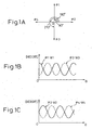
- Fig. 1A to Fig. and Fig. 2 are diagrams for explaining the principle of a phase-combining circuit (weighting circuit).
- Fig. 1A shows an example of input signals (input phases: ⁇ 1 to ⁇ 4) that are used in the phase-combining circuit
- Fig. 1B and Fig. 1C show weights (positive weights: W1 to W4) to be applied to the respective input signals.
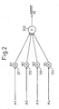
- reference numbers 211 to 214 denote multipliers and 202 denotes an adder.
- phase-combining circuit is applied to a timing signal generator circuit, for example, and the phase-combining circuit supplies at least three input phases (at least three input signals of different phases) directly to the phase-combining circuit without passing through a selector circuit, and generates a sum of the weighted phases.
- the phase-combining circuit uses, for example, four input phases ⁇ 1, ⁇ 2, ⁇ 3 and ⁇ 4 with a phase difference of 90 degrees between adjacent phases, as shown in Fig. 1A .
- the multipliers 211 to 214 give weights W1, W2, W3 and W4 to the respective input phases as shown in Fig. 1B and Fig. 2 .
- timing signal generator circuit of the above principle has three or more input phases, it is possible to cover an output phase range from 0 to 360 degrees based on only the weight control without changing over the input phases.
- the phase-combining circuit can also be implemented using single-end clocks or differential clocks.
- differential clocks there are different ways of counting phases depending on whether the clocks in a mutually complementing relationship are considered as one differential phase, or whether they are considered as two differential phases each having a 180-degree phase deviation, or whether they are considered as two phases of a single end with a phase deviation of 180 degrees. Therefore, in the present specification, the number of input phases (input signals) is counted by a weighting circuit that can apply different weights to the input phases. For example, three phases means that there are three phases to which mutually different weights can be applied by the phase-combining circuit.
- the effect of obtaining an output phase range from 0 to 360 degrees by using inputs of at least three phases can also be obtained by applying weights that change within a positive and negative range to phase inputs of at least two phases and adding up the weighted phases.
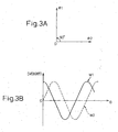
- Fig. 3A and Fig. 3B are diagrams for explaining a modification of the principle of the phase-combining circuit shown in Fig. 1A to Fig. 1C
- Fig. 3A shows an' example of phases (input phases ⁇ 1 and ⁇ 2) that are used in the phase-combining circuit
- Fig. 3B shows weights (weights having positive and negative signs: W1 and W2) to be applied to the respective phases.
- a phase-combining circuit is used that is not limited to the conventional phase interpolator.
- the conventional phase interpolator interpolates between selected two input phases and obtains an output.
- This interpolator is an amplifier circuit for a sum of the weighted input phases. This interpolator interpolates between the phases by successively changing the weight from a state where the weight is 100% given to a first phase to a state where the weight is 100% given to a second phase. When the amplifier circuit responds at a sufficiently high speed, a phase interpolated between the two input phases becomes the output phase.
- phase-combining circuit of the present invention can cover 0 to 360 degrees as the phase output range, the output phase of the phase-combining circuit does not need to be in between the two input phases. Accordingly, it is possible to use the phase-combining circuit that is not limited to the interpolator.
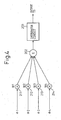
- Fig. 4 is a diagram for explaining a modification of the principle of the phase-combining circuit shown in Fig. 2 .
- reference numbers 211 to 214 denote multipliers
- 202 denotes an adder
- 203 denotes an integrator circuit.
- the phase-combining circuit (timing signal generator circuit) can be structured as an integration-type phase-combining circuit that uses the integrator circuit 203 in place of the amplifier circuit that has been used in the conventional phase interpolator, as shown in Fig. 4 .
- the multipliers 211 to 214 give weights W1 to W4 to respective input phases (input signals) ⁇ 1 to ⁇ 4.
- the adder 202 adds up the four weighted input phases (W1* ⁇ 1, W2* ⁇ 2, W3* ⁇ 3, and W4* ⁇ 4), and obtains the sum of the weighted phases (W1* ⁇ 1 + W2* ⁇ 2 + W3* ⁇ 3. +W4* ⁇ 4).
- the integrator circuit 203 integrates this sum of the weighted phases to combine the phases, thereby producing an output TS.
- the integrator circuit 203 integrates this sum of the weighted phases to combine the phases, thereby producing an output TS.
- a multi-input integrator circuit that can give different weights to individual input phases is used to obtain a weighted integration sum.
- the timing signal generator circuit has an advantage in that it is possible to obtain the whole phase range from 0 to 360 degrees based on inputs of a small number of phases. Therefore, it is not necessary to distribute a large number (for example, twelve phases) of clocks to each circuit (interpolator) while keeping a mutual phase relationship. Further, it is not necessary to provide a circuit for selecting an input phase. Therefore, it is possible to avoid an occurrence of a phase error attributable to a selecting circuit.
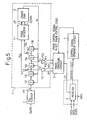
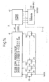
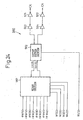
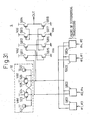
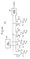
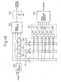
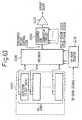
- Fig. 5 is a block diagram showing a timing signal generator circuit relating to the present invention.
- a reference number 1 denotes a four-phase clock generator circuit
- 2 denotes a PLL circuit
- 3 denotes a receiver
- 4 denotes a control signal generator circuit
- 5 denotes a phase-combining circuit (weighting circuit).
- a reference number 11 denotes a phase detector
- 12 denotes a charge pump
- 131 to 135 denote delayed stages
- 141 and 142 denote inverters
- 151 and 152 denote differential buffers.
- the first embodiment provides the timing signal generator circuit that generates a clock for the signal reception circuit (receiver 3) and that generates a receiver driving clock (timing signal) CK synchronous with a clock (data clock) that has been transmitted to the receiver 3 together with data.
- the timing signal generator circuit is constructed of the four-phase clock generator circuit that receives a reference clock clk synchronous with a clock supplied from the outside of the chip via the PLL circuit 2, the control signal generator circuit 4, and the phase-combining circuit 5.
- the output signal (timing signal) CK of the phase-combining circuit 5 is supplied to the receiver 3, for example, and the transmitted data is received.
- the receiver 3 compares the phase of the data clock supplied from the outside with the phase of the internal clock (the output of the timing signal generator circuit) CK.
- the receiver then feeds back a signal according to a result of the phase comparison to the phase-combining circuit 5 via the control signal generator circuit 4.
- the receiver 3 (signal reception circuit) is only one example, and the timing signal generator circuit of the present embodiment can also be applied to other various circuits (for example, a driver, a signal transmission circuit). While the output (reference clock clk) of the PLL circuit 3 is a single-phase signal in the first embodiment, it is also possible to structure such that the output signal is a differential (complementary) signal.
- the four-phase clock generator circuit 1 is structured in a PLL, which is constructed of the delayed stages 131 to 135, the phase detector 11, the charge pump 12, the inverters 141 and 142, and the differential buffers 151 and 152.
- the phase detector 11 sets a phase difference between a phase of a signal /Sa that is an output signal Sa of the delayed stage 132 inverted by the inverter 141 and a phase of a signal /Sb that is an output signal Sb of the delayed stage 134 inverted by the inverter 142, to 180 degrees ( ⁇ ).
- the phase detector 11 outputs to the charge pump 12 control signals (an up signal UP and a down signal DOWN) according to a difference between the phase of the signal /Sa (Sa) and the phase of the signal /Sb (Sb), and sets this phase difference to 180 degrees.
- the charge pump 12 generates a control voltage Vc according to the up signal UP and the down signal DOWN from the phase detector 11, and'applies this control voltage to the delayed stages 131 to 135.
- the charge pump 12 controls the difference between the phase of the signal Sa and the phase of the signal Sb so that this phase difference accurately becomes 180 degrees.
- the difference between the phase of the output signal Sa of the delayed stage 132 and the phase of the output signal Sc of the delayed stage 133 can be accurately set to 90 degrees.
- the delayed stages. 131 and 132 are for shaping the waveform of the reference clock clk.
- the delayed stage 135 is for giving a suitable load to the output of the delayed stage 134.
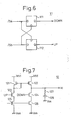
- Fig. 6 is a circuit diagram showing one example of the phase detector 11 in the four-phase clock generator circuit 1 of the timing signal generator circuit shown in Fig. 5 .
- the phase detector 11 is constructed of two latches 111 and 112.
- the latch 111 having the inverted output /Sb of the delayed stage 134 as a trigger takes in the inverted output /Sa of the delayed stage 132.
- the latch 112 having the inverted output /Sa of the delayed stage 132 as a trigger takes in the inverted output /Sb of the delayed stage 134.
- the phase detector 11 generates the down signal DOWN and the up signal UP as the outputs of the latches 111 and 112 respectively, and supplies these signals to the charge pump 12.
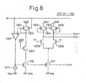
- Fig. 7 is a circuit diagram showing one example of a charge pump in the four-phase clock generator circuit 1 of the timing signal generator circuit shown in Fig. 5 .
- the charge pump 12 is constructed of p-channel MOS transistors (p-MOS transistors) 121 and 122, n-channel MOS transistors (n-MOS transistors) 123 to 126, a resistor 127, and a capacitor 128.
- the charge pump 12 receives the up signal UP and the down signal DOWN as the outputs of the phase detector 11 by the pair of differential transistors 123 and 124 respectively, and outputs the control voltage Vc.
- the control voltage Vc is applied to all the delayed stages 131 to 135 to control the delay volume of each delayed stage.
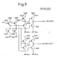
- Fig. 8 is a-circuit diagram showing one example of a delayed stage 130 (131 to 135) in the four-phase clock generator circuit 1 of the timing signal generator circuit shown in Fig. 5 .
- the delayed stage 130 is constructed of p-MOS transistors 1301 to 1306, n-MOS transistors 1307 to 1311, a differential amplifier 1312, and a load 1313.
- the control voltage Vc is applied to a negative load of the differential amplifier 1312, and is also applied to a gate of the transistor 1302.
- a positive input of the differential amplifier 1312 is connected to a common connection node of a gate and a drain of the transistor 1301 provided in parallel with the transistor 1302.
- Vcn denotes a bias voltage of the transistors 1310 and 1311
- V+(V-) denotes an input signal (an output of the preceding delayed stage (PLL circuit))
- out+(out-) denotes an output signal (an input to the next delayed stage).
- the signals Sa and Sc that have a correct phase difference of 90 degrees are supplied to the differential buffers 151 and 152 respectively, so that the differential buffers 151 and 152 produce four-phase clocks ⁇ 1 to ⁇ 4 each having a phase difference of 90 degrees between adjacent clocks.
- Fig. 9 is a circuit diagram showing one example of a differential buffer 150 (151, 152) in the four-phase clock generator circuit 1 of the timing signal generator circuit shown in Fig. 5 .
- the differential buffers 151 and 152 are constructed of p-MOS transistors 1501 to 1506 and n-MOS transistors 1507 to 1512 respectively, to generate the signals ⁇ 1, ⁇ 3 ( ⁇ 2, ⁇ 4) having a phase difference of 180 degrees from the signal Sa (Sc).
- the four-phase clock generator circuit 1 generates the four-phase clocks ⁇ 1 to ⁇ 4 each having a phase difference of 90 degrees between adjacent clocks, in the manner as described above, and supplies them to the phase-combining circuit 5.
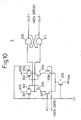
- Fig. 10 is a circuit diagram showing one example of the receiver 3 in the timing signal generator circuit shown in Fig. 5 .
- the receiver 3 At a rise of the clock (internal clock CK), a decision is made about data input (in+, in-).
- the receiver 3 has a phase comparator similar to that for receiving data (decision), and the phase comparator decides a phase relationship between the internal clock CK and the data clock. Then, the receiver 3 feedback-controls the internal clock CK via the control signal generator circuit 4 and the phase-combining circuit 5 as described later.
- the receiver 3 is constructed of p-MOS transistors 301 to 304; n-MOS transistors 305 to 309, and NAND gates 310 and 311.
- Data (differential signals in+ and in-) that have been transmitted are supplied to differential inputs (gates of the transistors 307 and 308), and are driven (decided) by the internal clock (output of the timing signal generator circuit) CK.
- Data (OUT+ and OUT-) are output via the latch circuits (NAND gates 310 and 311).
- the internal clock CK is at a low level "L"
- the transistors 301 and 304 are turned on and the transistor 309 is turned off, so that a pre-charging is carried out.
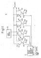
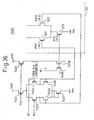
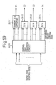
- Fig. 11 is a circuit diagram showing one example of the phase-combining circuit 5 in the timing signal generator circuit shown in Fig. 5 .
- the phase-combining circuit 5 is constructed of pairs of differential transistors 501, 502, 504, 505, 507, 508, 510 and 511 supplied with clocks (input phases) ⁇ 1, ⁇ 3, ⁇ 2, ⁇ 4, ⁇ 3, ⁇ 1, ⁇ 4, ⁇ 2 respectively, transistors 503, 506, 509 and 512 supplied with weights (weight signals) W1, W2, W3 and W4 at gates respectively, a weight signal generator circuit 51 for generating the weight signals W1 to W4, and a load device 12 connected in common to each of the pairs of differential of transistors.
- phase control codes are supplied from the control signal generator circuit 4 to the weight signal generator circuit 51.
- the weight signal generator circuit 51 generates the weight signals W1 to W4 corresponding to the phase control signals. These weight signals W1, W2, W3 and W4 are supplied to the gates of the transistors 503, 506, 509 and 512, so that currents proportional to the weight signals flow.
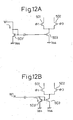
- Fig. 12A and Fig. 12B are diagrams for explaining a method of giving a weight in the control signal generator circuit shown in Fig. 11 .
- Fig. 12A and Fig. 12B show.the transistor 503 and the pair of differential transistors 501 and 502 that are supplied with the weight W1 to their gates respectively. The rest of the weights W2, W3 and W4 are also given in a similar manner.
- the weight W1 (W1 to W4) is given as an output current of a D/A converter for digital-to-analog converting a control code, for example.
- This current (weight) W1 flows to a diode-connected transistor 503'.
- a gate voltage same as that of the transistor 503' is applied to the transistor 503 to give the weight (the current W1 flows).
- Fig. 12A shows a state that the transistor 503' is provided in the weight signal generator circuit 51.
- the transistor 503' may be provided adjacent to the transistor 503, as shown in Fig. 12B .
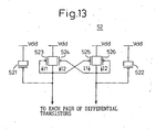
- Fig. 13 is a circuit diagram showing one example of a load device 52 in the phase-combining circuit 5 shown in Fig. 11 .
- the load device 52 in the phase-combining circuit 5 is constructed of capacitors (MOS capacitor) 521 and 522 and p-MOS transistors 523 to 526.
- the integration capacitor (521 and 522) are added to the cross-coupled p-MOS loads (523 to 526) having a differential impedance in high resistance.
- I1 + I2 flows to each pair of differential transistors
- the cross-coupled p-MOS load shows a high impedance for a differential signal.
- the cross-coupled p-MOS load shows a low impedance for an in-phase signal.
- Fig. 14 is a block circuit diagram showing one example of the control signal generator circuit 4 in the timing signal generator circuit shown in Fig. 5 .
- a reference number 41 denotes an up-down signal generator circuit
- 42 denotes an up-down counter
- 430 to 437 denote registers.
- a reference number 530 denotes the weight signal generator circuit 51 (D/A converter) in the phase-combining circuit 5.
- the timing signal generator circuit is for generating a receiver driving clock (internal clock CK) synchronous with the data clock that has been transmitted to the receiver 3 together with the data.
- a phase comparator compares the phase of the data clock with the phase of the internal clock CK.
- the phase comparator is one similar to that for receiving data (decision). By driving a decision circuit with the internal clock CK, a phase relationship (an advance or a delay: DD) between the internal clock CK and the data clock is decided.
- An advance or delay DD is sequentially stored in eight registers 430 to 437, for example, and results of decisions DD0 to DD7 for eight cycle clocks are taken into the up-down signal generator circuit 41.
- the up-down signal generator circuit 41 generates an up signal UP and a down signal DOWN based on a difference of numbers of "1" and "0" of each of the results of decisions DD0 to DD7.
- the up signal UP and the down signal DOWN are supplied to the up-down counter 42, and they are converted into control codes (for example, six bits).
- the control codes from the up-down counter 42 are supplied to the weight signal generator circuit 51 (D/A converter 530) in the phase-combining circuit 5.
- the D/A converter 530 may be structured as a look-up table of a ROM or the like to output the weight signals (W1 to W4) corresponding to the supplied control codes.
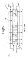
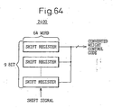
- Fig. 15 is a block circuit diagram showing one example of the up-down counter 42 in the control signal generator circuit shown in Fig. 14 .
- a reference number 421 denotes a shift register
- 422 and 423 denote inverters.
- the up-down counter 42 shown in Fig. 15 is structured as a Johnson counter that is shift-controlled by a clock clk'. For example, out of 16-bit data from b1 to b16, at an initial state, the first half eight bits (b1 to b8) are set to "1" (high level “H"), and the latter half eight bits (b9 to b16) are set to "0" (low level “L”).
- the up-down signal generator circuit 41 has input an up signal UP
- the data of the bit b16 is inverted by an inverter 422, and is shifted to the right so that the inverted data is written into the bit 1.
- Fig. 15 shows an example that the bits b1 to b5 are "1" and the bits b6 to b16 are "0".
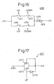
- Fig. 16 is a circuit diagram showing one example of a clock generator circuit 4210 for supplying a clock signal to the up-down counter shown in Fig. 15 .
- the clock clk' to be used in the shift register 421 can be constructed of a switch 4211 that is controlled by an up signal UP, a switch 4212 that is controlled by a down signal DOWN, a switch 4213 that is controlled by an inverted up signal /UP, a switch 4214 that is controlled by an inverted down signal/DOWN, and inverters 4215 and 4216.
- Fig. 17 is a circuit diagram showing an example of a structure of the switch4211 in the clock generator circuit shown in Fig. 16 .
- the switch 4211 is structured by a transfer gate consisting of a p-MOS transistor 4211, an n-MOS transistor 42112, and an inverter 42113.
- the switch 4211 is turned on.
- Other switches 4212 to 4214 also have a similar structure.
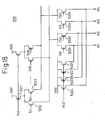
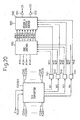
- Fig. 18 is a circuit diagram showing one example of the D/A converter shown in Fig. 14 .
- the D/A converter 530 analog-to-digital converts complementary control codes b1, /bi to b16 and /b16 to output four weights (currents) W1 to W4.
- the control codes b1 and /b1 are supplied to the gates of the p-MOS transistors 5312 and 5313, and other codes b2, /b2 to b16 and /b16 are also supplied to gates of similar transistors. Currents that flow through these transistors are added up and they are output as the weights (currents) W1 to W4 via the transistors 5331 to 5334.
- a bias voltage Vcp is applied to the gate of the transistor 5311.
- the bias voltage is also applied to other corresponding transistors.
- a bias voltage Vcp' is applied to the gates of the transistors 5321 to 5324 respectively.
- the transistors 5321 to 5324 add predetermined bias currents to the weights W1 to W4 to ensure the operation of the circuit that gives the weights.
- the transistors 5331 to 5334 that control currents based on the control codes b1, /b1 to b16 and /b16 and output the weights W1 to W4 are further controlled by other control codes (weight selection control signals) b0 and /b0.
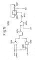
- Fig. 19 is a circuit diagram showing one example of a circuit for generating a weight selection control signal to be used in the D/A converter shown in Fig. 18 .
- a circuit 5000 for generating the weight selection control signal b0 (/b0) is constructed of NAND gates 5001 to 5004, inverters 5005 to 5007, and a flip-flop 5008. Based on this structure, the circuit 5000 generates the weight selection control signal b0 from a control code b16, an up signal UP, a down signal DOWN and a clock clk.
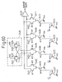
- Fig. 20 is a block circuit diagram showing one example of a phase-combining circuit of a timing signal generator circuit.
- a reference number 530 denotes a D/A converter
- 541 to 544 denote weight processing circuits
- 550 denotes a pre-driver
- 560 denotes a mixer and output buffer.
- the phase-combining circuit 5 is constructed of the D/A converter 530, the weight processing circuits 541 to 544, the pre-driver 550, the mixer and output buffer 560, and inverters 571 and 572.
- the D/A converter 530 is applied with inputs of a reference current Ir and a plurality of control codes such as, for example, complementary 18-bit control codes CD0, /CD0 to CD8 and /CD8, and CD10, /CD10 to CD18 and /CD18.
- the D/A converter 530 then outputs four weights (currents) W1 to W4 corresponding to these control codes.
- a reference symbol TES denotes a testing signal that is used for testing a circuit.
- the weight processing circuits 541 to 544 receive the weights W1 to W4, and produces outputs (W11 to W41) for the pre-driver 550 linked to these'weights W1 to W4 and outputs (W12 to W42) for the mixer and output buffer 560.
- the pre-driver 550 receives different input phases (such as, for example, four-phase input signals each having a 90-degree phase difference between adjacent phases) ⁇ 1 to ⁇ 4, and the weight-signals W11 to W41 for the pre-driver, and outputs adjusted input phases (input signals of different phases) ⁇ W1, / ⁇ W1 to ⁇ W4 and / ⁇ W4.
- the mixer and output buffer 560 receives the weight signals W12 to W42 for the mixer and output buffer, and the adjusted input phases ⁇ W1, / ⁇ W1 to ⁇ W4 and / ⁇ W4 from the pre-driver 550, and outputs the internal clocks (timing signals) CK and /CK via the inverters 571 and 572.
- Fig. 21 is a circuit diagram showing one example of the D/A converter 530 in the phase-combining circuit shown in. Fig. 20 .
- the D/A converter 530 is constructed of a p-MOS transistor 5300 to which the reference current Ir -flows, a p-MOS transistor 5301 that is current-mirror-connected with the transistor 5300, and switch p-MOS transistors 5302 and 5303 to which the control codes (CD0 and /CD0) have been supplied at their gates.
- the transistors 5301 to 5303 are provided for each-complementary control code (CD0, /CD0; CD1, /CD1; --- CD8, /CD8, and CD10, /CD10; CD11, /CD11;-CD18, /CD18).
- the p-MOS transistor 5304 that is current-mirror-connected with the transistor 5300 gives a bias current to the weight (current) W1.
- the D/A converter 530 digital-to-analog converts the control codes CD0, /CD0 to CD8 and /CD8, and CD10, /CD10 to CD18 and /CD18, and outputs the weights (currents) W1 to W4.
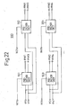
- Fig. 22 is a block circuit diagram showing one example of the pre-driver 550 in the phase-combining circuit shown in Fig. 20 .
- the pre-driver 550 is constructed of a pre-driver unit 551 that receives the weight signal W11 for the pre-driver and the phase signals ⁇ 1 and ⁇ 3 and outputs the adjusted input phases (input signals of mutually different phases) ⁇ W1 and ⁇ W3, a pre-driver unit 552 that receives the weight signal W21 and the phase signals ⁇ 1 and ⁇ 3 and outputs the adjusted input phases / ⁇ W1 and / ⁇ W3, a pre-driver unit 553 that receives the weight signal W31 and the phase signals ⁇ 2 and ⁇ 4 and outputs the adjusted input phases ⁇ W2 and ⁇ W4, and a pre-driver unit 554 that receives the weight signal W41 and the phase signals ⁇ 2 and ⁇ 4 and outputs the adjusted input phases / ⁇ W2 and / ⁇ W4.
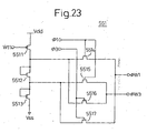
- Fig. 23 is a circuit diagram showing one example of the pre-driver unit 551 in the pre-driver shown in Fig. 22 .
- the pre-driver unit 551 is constructed of a p-MOS transistor 5511 and n-MOS transistors 5512 to 5517.
- the weight signal W11 for the pre-driver is supplied to the gate of the transistor 5511, and the phase signals ⁇ 1 and ⁇ 3 are supplied to the gates of the transistors 5514 and 5515 and the gates of the transistors 5516 and 5517 respectively.
- the pre-driver unit 551 takes out the adjusted input phase ⁇ W1 from a common source of the transistors 5514 and 5517, and takes out the adjusted input phase ⁇ W3 from a common source of the transistors 5515 and 5516.
- the adjusted input phases ⁇ W1 and ⁇ W3 are output with their amplitudes and DC levels adjusted so as to be suitable for a mixer section 561 in the mixer and output buffer to be described later.
- Other pre-driver units 552 to 554 are also structured to have a similar construction to that of the pre-driver unit 551 except their input and output signals.
- Fig. 24 is a block circuit diagram showing one example of the mixer and output buffer 560 in the phase-combining circuit shown in Fig. 20 .
- the mixer and output buffer 560 is constructed of a mixer section 561, an output buffer section 562, and inverters 563 and 564.
- the mixer section 561 receives the adjusted input phases ⁇ W1, / ⁇ W1 to ⁇ W4 and / ⁇ W4, and the weight signals W12 to W42 for the mixer and output buffer, and supplies output signals trclk and /trclk to the output buffer section 562.
- the mixer section 561 adds (multiplies) the weight signals W12 to W42 to the input phases ⁇ W1, / ⁇ W1 to ⁇ W4 and / ⁇ W4, and sums up these weighted signals and integrates a result.
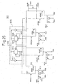
- Fig. 25 is a circuit diagram showing one example of the mixer section 561 in the mixer and output buffer shown in Fig. 24 .
- the mixer section 561 includes a load device 5610, a pair of differential transistors 611 and 612 that have been supplied at their gates with the adjusted input phases ⁇ W1 and ⁇ W3 from the pre-driver 550, and a transistor 613 that has been supplied at its gate with the weight signal W12 for the mixer and output buffer from the weight processing circuit 541.
- the gate (weight signal W12) of the transistor 613 is connected with the gate and the drain of the transistor 614 and one end of a MOS capacitor 615.
- the structures of the transistors 611 to 615 taken for the input phases ⁇ W1 and ⁇ W3 and the weight signal W12 are also provided in a similar manner for other input phases / ⁇ W3 and / ⁇ W1 and the weight signal W22, the input phases ⁇ W2 and ⁇ W4 and the weight signal W32, and the input phases / ⁇ W4 and / ⁇ W2 and the weight signal W42.
- the load device 5610 has a structure similar to that of the load device 52 explained with reference to Fig. 13 .
- the load device 5610 is constructed of MOS capacitors 5611 and 5612, and p-MOS transistors 5613 to 5616.
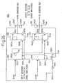
- Fig. 26 is a circuit diagram showing one example of the output buffer section 562 in the mixer and output buffer shown in Fig. 24 .
- This circuit is called a supply-insensitive buffer in which a delay is not much dependent on a power source voltage.
- the output buffer section 562 is constructed of p-MOS transistors 5621 to 5628, n-MOS transistors 5651 to 5660, and an inverter 5661.
- the output buffer section 562 amplifies an input signal of a small amplitude (trclk, /trclk), and produces an output signal of a large amplitude (full CMOS amplitude).
- a reference symbol RST denotes a reset signal.
- the reset signal RST is set to a low level "L" at the time of resetting the circuit.
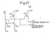
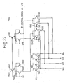
- Fig. 27 is a circuit diagram showing one example of the weight processing circuit 541 in the phase-combining circuit shown in Fig. 20 .
- the weight processing circuit 541 is constructed of p-MOS transistors 5411 and 5412, and n-MOS transistors 5413 and 5414.
- the weight processing circuit 541 processes the weight (current) W1 from the D/A converter 530, and produces a weight signal W11 (voltage) suitable for the pre-driver section 550 (gate input of the p-MOS transistor 5511 shown in Fig. 23 ), and a weight signal W12 (current) suitable for the mixer section 561 (common connection mode of the transistors 613 and 614 and the capacitor 615 shown in Fig. 25 ) of the mixer and output buffer.
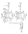
- Fig. 28 is a circuit diagram showing another example of a four-phase clock generator circuit (reference number 1 in Fig. 5 ) in a timing signal generator circuit.
- the four-phase clock generator circuit 1 for driving the phase-combining circuit 5 is constructed of a load device consisting of integrated capacitors 101 and 102 and cross-coupled p-MOS loads 103 to 106, a pair of differential amplifiers 107 and 108, a n-MOS transistor 109 that has applied to it a bias voltage Vcn at its gate, cross-coupled p-MOS loads 161 to 164, a pair of differential amplifiers 165 and 166, a n-MOS transistor 167 that has applied to it a bias voltage Vcn at its gate, and clock buffers 171 and 172.
- the four-phase clock generator circuit 1 shown in Fig. 28 generates four signals (phases) ⁇ 1, ⁇ 2, ⁇ 3 and ⁇ 4 each having a 90-degree phase difference between adjacent phases, from differential reference clocks (clk and /clk) supplied from the PLL circuit 2.
- the four-phase clock generator circuit 1 generates the signals ⁇ 2 and ⁇ 4 that have phases of 90 degrees and 270 degrees respectively from the input phases (0 degree and its complement of 180 degrees) by using a 90-degree phase shifter using an integrator circuit.
- These phases ⁇ 1, ⁇ 2, ⁇ 3 and ⁇ 4 are regarded as differential four-phase signals, and an increase in the number of phase is defined as a direction in which a delay increases.
- the four-phase clocks can also be supplied directly from the PLL circuit.
- the phase-combining circuit (refer to the phase-combining circuit 5 shown in Fig. 11 (refer to the pre-driver unit 551 shown in Fig. 23 and the mixer section 561 shown in Fig. 25 )) has such a structure that the pairs of differential transistors 501 to 503 and 611 to 614 are provided for the four input'phases ⁇ 1 to ⁇ 4 respectively, and tail currents of respective phase signals are'controlled by the currents (W1 to W4; W11 to W41; and W12 to W42) supplied from the D/A converter (51; 530).
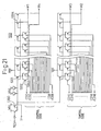
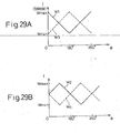
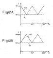
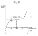
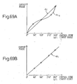
- Fig. 29A and Fig. 29B are diagrams showing one example of a change in the weight in the timing signal generator circuit.
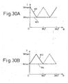
- Fig. 30A and Fig. 30B are diagrams showing another example of a change in the weight in the timing signal generator circuit.
- Fig. 29A and Fig. 30A show the weights W1 and W3
- Fig. 29B and Fig. 30B show the weights W2 and W4.
- the weights W1 to W4 (output currents of the weight signal generator circuit 51 or the D/A converter 530) in the phase-combining circuit 5 change as shown in Fig. 29A and Fig. 29B , for example.
- a vertical axis I shows a current
- a horizontal axis ⁇ shows an output phase of the phase-combining circuit.
- the output phase when the weight W1 takes a maximum value Wmax is the origin of the phase.
- each weight Wn (W1 to W4) takes Wmax as a maximum value and Wmin as a minimum value.
- Each output phase takes a non-zero value (including a predetermined bias current).
- the weights (currents) W1 to W4 generated by the D/A converter 530 include a predetermined (Wmin) bias current according to the transistors 5321 to 5324.
- Fig. 29A shows an example of triangular waves in which the phases of the weights W1 and W3 are inverted (deviated by 180 degrees).
- Fig. 29B shows an example of waveforms in which the phases of the weights W2 and W4 are delayed by 90 degrees from the weights W1 and W3 respectively.
- each weight Wn (W1 to W4) may be formed in a triangular wave with its lower half clamped.
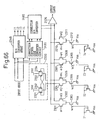
- Fig. 31 is a block circuit diagram showing one example of a phase-combining circuit as a timing signal generator circuit. This shows a modification of the phase-combining circuit shown in Fig. 11 .
- the load device 52 is similar to that shown in Fig. 11 , and the pairs of differential amplifiers 5801 to 5804 correspond to the transistors 501, 502 to 510 and 511 shown in Fig. 11 .
- the phase-combining circuit 5 has an output buffer consisting of p-MOS transistors 5811 to 5814 and n-MOS transistors 5815 to 5818, in the phase-combining circuit shown in Fig. 11 .
- This output buffer is a supply-insensitive buffer circuit in which a delay is not very dependent on a power source voltage Vdd.
- This circuit corresponds to the output buffer section 562 shown in Fig. 26 that amplifies a signal of a small amplitude and outputs a signal of a large amplitude.
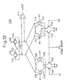
- Fig. 32 is a circuit diagram showinga phase-combining circuit as a the timing signal generator circuit.
- a phase-combining circuit 7100 uses two input phases ⁇ 1 and ⁇ 2, and is constructed of p-MOS transistors 7101 to 7104, n-MOS transistors 7105 to 7116, and a comparator (differential amplifier) 7117.
- the transistors 7105, 7106, 7108, 7109, 7111, 7112, 7114 and 7115 constitute pairs of differential amplifiers respectively. These transistors give the weight W1 to the gate of the transistor 7107, give the weight W2 to the gate of the transistor 7116, and give a fixed weight W0 to the gates of the transistors 7110 and 7113 respectively.
- the four phases ( ⁇ 1 to ⁇ 4: ⁇ 1, / ⁇ 1 to ⁇ 4, / ⁇ 4) are not input as in the phase-combining circuit 5 shown in Fig. 11 , but the two phases ( ⁇ 1, ⁇ 2: ⁇ 1, / ⁇ 1, ⁇ 2, / ⁇ 2) are input. These two phases are weighted with both polarities of positive and negative, thereby to obtain the outputs that cover the whole phase range from 0 to 360 degrees. It is also possible to give two phases of ⁇ 1 and ⁇ 2 to the phase-combining circuit 5 shown in Fig. 11 and to give weights having signs to these phases thereby to cover the whole phase range.
- phase-combining circuit since it is possible to give different weights to the four phases in the phase-combining circuit shown'in Fig. 11 , the input of the four phases has been assumed. On the other hand, in the case of the phase-combining circuit here, the input of two phases has been assumed, as there are only two weights that can be controlled. It is preferable that the phase signals ⁇ 1 and ⁇ 2 have a phase difference of 90 degrees. However, the phase signals can be used so long as their phases are deviated.
- the phase-combining circuit 7100 has the pairs of differential transistors (7108 and 7109; 7111 and 7112) to which the fixed weight W0 has been supplied respectively, and the pairs of differential transistors (7105 and 7106; 7114 and 7115) to which the externally-controlled weights W1 and W2 have been supplied respectively.
- the pairs of differential transistors applied with the fixed weight and the pairs of differential transistors applied with the variable weights have their output lines mutually inverted. Therefore, the pairs of differential transistors supplied with the fixed weight give opposite polarity to the pairs of differential transistors applied with the variable weights.
- the variable weight Wi (W1, W2) is smaller than the fixed weight W0, an effective weight (Wi - W0) takes a negative value.
- an effective weight (Wi - W0) takes a positive value.
- the output (OUT) is given as an output of the comparator 7117.
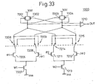
- Fig. 33 is a circuit diagram showing one example of a phase-combining circuit as a timing signal generator circuit.
- a phase-combining circuit 7200 uses two input phases ⁇ 1 and ⁇ 2 in a similar manner to Fig. 32 .
- the phase-combining circuit 7200 is constructed of p-MOS transistors 7201 to 7204, n-MOS transistors 7205 to 7207 and 7211 to 7213, polarity switches 7208, 7209 and 7214, 7215, and a differential amplifier 7210.
- the transistors 7205, 7206 and 7211, 7112 constitute pairs of differential transistors respectively.
- the polarity switches 7208, 7209 and 7214, 7215 invert polarities of the pairs of differential transistors that give weights.
- control code is a 6-bit code
- the control code may be so arranged that the upper two bits are for controlling the polarity switches 7208, 7209 and 7214, 7215, and other four bits are for controlling the weighting of the D/A converter 530.
- the polarity switches have weight-controlling digital values expressed in a signed binary, for controlling weights using the sign bits.
- the output (OUT) is given as an output of the differential amplifier 7210.
- the phase-combining circuit 7200 uses always one kind of clock signal (input phase ⁇ 1, / ⁇ 1; ⁇ 2, / ⁇ 2) that is input to the pairs of differential transistors. Therefore, there is no disturbance in the operation of the pairs of the differential transistors attributable to a phase selection. Further, when the phase-combining circuit is used in a clock synchronizing circuit, the phase value changes by every step based on the UP signal and the DOWN signal. Further, when the polarity of the weight changes inside the phase-combining circuit, the value of the weight is always zero. Therefore, the influence that the polarity inversion applies to the operation inside the phase-combining circuit is extremely small.
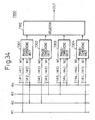
- Fig. 34 is a circuit diagram showing one example of a phase-combining circuit as a timing signal generator circuit
- Fig. 35 is a diagram showing one example of a change in the weight in the phase-combining circuit shown in Fig. 34 .
- the phase-combining circuit is constructed of a plurality of (four) phase-combining units 7301 to 7304, and a selector 7310.
- the four phase-combining units 7301, 7302, 7303 and 7304 are for combining two input phases ( ⁇ 1, ⁇ 2: ⁇ 1, / ⁇ 1; ⁇ 2, / ⁇ 2), ( ⁇ 2, ⁇ 3), ( ⁇ 3, ⁇ 4), and ( ⁇ 4, ⁇ 1), based on the weights W1 and W2 respectively.
- Outputs of these four phase-combining units 7301 to 7304 are produced via the selector 7310.
- the weights W1 and W2 change as shown in Fig. 35 , for example.
- one of outputs of the phase-combining units 7301 to 7304 is selectively produced according to a range of the control code.
- the phase-combining units 7301 and 7303 and the phase-combining units 7302 and 7304 operate in mutually completely opposite phase signals respectively. Therefore, it is also possible to structure the whole phase-combining circuit using only two phase-combining units by exchanging the polarities of the outputs.
- phase-combining circuit 7300 an input phase is supplied to each of the phase-combining units 7301 to 7304 without' using a changeover switch or a selector circuit. Therefore, the signals input to the pairs of differential transistors are always completely cyclical signals of the same phase. As a result, there is no disturbance in the operation of the pairs of the differential transistors attributable to a phase selection.
- Fig. 36 is a circuit diagram showing one example of a pre-driver in a phase-combining circuit as a timing signal generator circuit. This shows an example of the pre-driver that gives signals (input phases ⁇ 1 and ⁇ 3, and the weight W1) to the pairs of differential transistors 501, 502 and 503 of the phase-combining circuit shown in Fig. 11 .
- clock signals for example, input phases ⁇ 1 and ⁇ 3 for driving pairs of transistors that carry out the weighting have been in a constant amplitude irrespective of whether the signals are in a small amplitude or a large amplitude.
- the input phases ( ⁇ 1 and ⁇ 3) supplied to the gates of the pairs of differential transistors have a constant amplitude regardless of the value of the weight (for example W1). Therefore, there has been a problem that a current waveform that appears in the output of the weighting circuit is not scaled in proportion to the weight. Further, when an input voltage that is larger than an input voltage sufficiently large for suitably carrying out a current steering of the pairs of differential transistors has been applied, a dead time occurs.
- a pre-driver 7400 of the seventh embodiment is, for example, suitable for processing and supplying the signals (input phases ⁇ 1 and ⁇ 3 and the weight W1) to the transistors 501, 502 and 503 in the phase-combining circuit shown in Fig. 11 .
- the pre-driver 7400 is constructed of p-MOS transistors 7401 to 7404 and n-MOS transistors 7405 to 7409.
- the transistors 7401 to 7409 are used for processing the signals (input phases ⁇ 1 and ⁇ 3 and the weight W1) to the transistors 501, 502 and 503 in the phase-combining circuit shown in Fig. 11 .
- four similar structures are provided for four pairs of differential transistors (four weights).
- the input clock signals (input phases ⁇ 1 and ⁇ 3) are first input to a level converter circuit (pre-driver) having the p-MOS pair of differential transistors 7403 and 7404 of the tail current proportional to the weight W1.
- the load device of the level converter circuit consists of the two diode-connected n-MOS transistors 7405 and 7406 and the diode-connected n-MOS transistor 7407 connected to the source of these transistors.
- a mirror ratio is selected so that the pairs of the differential transistors generate a voltage slightly larger than the voltage that is sufficient for switching the current.
- Phase signals ⁇ W1 and ⁇ W3 obtained based on the processing with the weight W1 are supplied to the pairs of differential transistors 501 and 502.
- the weight (current) W1 from the D/A converter 530 flows to the transistor 7408, and a weight W12 obtained by processing via the transistor 7409 is supplied to the gate of the transistor 503.
- a weighted differential current'wave that is integrated by the phase-combining - circuit is scaled so that this current wave is more proportional to the weight.
- the linearity of the phase characteristic with respect to the control code is improved.
- the power source voltage Vdd has varied, there is little variation in the voltage level that is input to the pairs of differential transistors of the phase-combining circuit and the common mode voltage. Therefore, it is possible to provide a circuit having small timing variation against a change in the power source voltage Vdd.
- an input signal is also small. Therefore, noise due to capacitive coupling also becomes smaller at a constant rate.
- the noise due to a capacity coupling appears relatively large for a small weight. This also improves the linearity of the phase characteristic with respect to the control code.
- Fig. 37 is a circuit diagram showing one example of a weight signal generator circuit in a phase-combining circuit as a timing signal generator circuit . This shows an example where a phase is designated by a six-bit digital control signal.
- a weight-signal generator circuit 7500 has sixteen constant-current sources constructed of p-MOS transistors 7501 to 7503 and an inverter 7504.
- the weight signal generator circuit 7500 converts the lower four bits (CB0 to CB3) of a six-bit control signal into sixteen control codes (thermometer codes) b1 to b16, and changes over currents of respective constant-current sources to generate complementary control currents.
- the upper two bits CB4 and CB5 are applied directly and via inverters 7523 and 7533 to control p-MOS transistors 7521, 7522. 7531 and 7523, to generate weights (currents) W1 to W4 from the complementary control currents.
- p-MOS transistors 7511 to 7514 for giving bias currents (for example, corresponding to Wmin in Fig. 29A and Fig. 29B ) not dependent on control codes, to the weights W1 to W4 respectively.
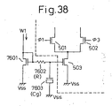
- Fig. 38 is a circuit diagram showing a modified example of pairs of differential transistors to be applied to a phase-combining circuit. This shows a modified example of pairs of differential transistors 501 to 503 shown in Fig. 11 .
- the weight W1 flows to a p-MOS transistor 7601 of which gate and drain are connected in common (diode connected), and is also supplied to the gate of a transistor 503 via a resistor 7602.
- the gate of the transistor 503 is connected to a low-potential power source Vss via a capacitor 7603.
- the gate voltage of the transistor 503 for controlling the tail current of the pairs of differential transistors is generated by a filter circuit consisting of the diode-connected transistor 7601, the resistor 7602, and the capacitor 7603.
- the weight currents of the pairs of differential transistors are not changed instantly even if the control codes have changed, but are changed within a clock cycle period, for example.
- the time constant of the resistor 7602 (R) and the capacitor 7603 in the filter circuit is set to a time of about the clock cycle. Pairs of differential transistors for other weights W2 to W4 also have a similar structure.
- a circuit that receives a signal operates at a correct timing with the signal.
- a method of generating a correct timing there has been a method of providing a phase-variable timing signal generator circuit that uses a phase interpolator in the feedback loop like a DLL or PLL as described above.
- ⁇ 180 degrees
- ⁇ /2 90 degrees
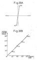
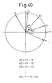
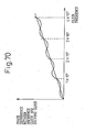
- Fig. 39A and Fig. 39B are diagrams for explaining a problem when a phase of an input signal to be used in the phase-combining circuit has been deviated.
- Fig. 39A shows a state that a phase between differential clock signals (between signals ⁇ 1 and ⁇ 3, and between signals ⁇ 2 and ⁇ 4) has been deviated from a predetermined value when the two sets of differential clock signals ( ⁇ 1, ⁇ 3; ⁇ 2, ⁇ 4) are used as input signals of four phases.
- Fig. 39B shows a relationship between the phase control codes and the actual output phases in this case.
- the above-described phase-combining circuit shown in Fig. 11 uses the two sets of differential clock signals ( ⁇ 1, ⁇ 3; ⁇ 2, ⁇ 4) as input signals of four phases in the phase-combining circuit.
- the phase interpolator circuit (phase-combining circuit) integrates and compares a sum of the weighted inputs of these input signals, and generates clocks of phases corresponding to the weight values (W1 to W4). In other words, the phase interpolator shifts the weight from a first phase to a second phase thereby to generate a clock of an intermediate phase between the two phases.
- the precision of the output of the phase interpolator is limited by the precision of the reference phases (phases of the input signals ⁇ 1 to ⁇ 4) that are given to the inputs.
- phase characteristic with respect to the control code (the phase characteristic of a signal actually output with respect to the control code) is deviated from a straight line as shown in Fig. 39B .
- the signal transmission speed is a high speed of a few Gbps, such as, for example, 2.5 Gbps
- an error of a reception timing generator circuit timing signal generator circuit
- a deviation of a phase difference of a differential signal used for the reference clocks (input signals of the phase-combining circuit) from the ideal value (90 degrees) also needs to be restricted to a small value of 10 to 20 ps in terms of time.
- the input signals (two sets of differential signals) of four phases that are used as the reference clocks must be generated so that a mutual phase difference is accurately 90 degrees. It is furthermore necessary to transfer the generated signals to the phase interpolator by keeping this phase difference.
- Fig. 40 is a diagram for explaining the principle of a timing signal generator circuit.
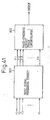
- Fig. 41 is a block diagram schematically showing the timing signal generator circuit shown in Fig. 40 .
- a reference number 801 denotes an input signal processing circuit
- 802 denotes a phase-combining circuit (phase interpolator).
- the input signal processing circuit 801 processes n input signals (f1 to fn), generates n signals (F1 to Fn), and supplies the processed signals (F1 to Fn) to the phase-combining circuit 802.
- the signals to be combined together are not limited to adjacent two signals (f1 and f2, f2 and f3, ---) or three signals (f1, f2, f3, and f2, f3, f4, ---). It is also possible to combine two signals by skipping a predetermined number like (f1 and f3, f2 and f4, ---) or three signals like (f1, f3, f5, and f2, f4, f6, ---), for example. Further, it is also possible to obtain intermediate phases (signals F1, F2, ---) by combining any optional k signals without limiting to two or three phases.
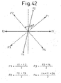
- Fig. 42 is a diagram for explaining one operation principle of a timing signal generator circuit.
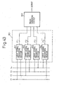
- Fig. 43 is a block circuit diagram schematically showing a timing signal generator circuit to which the operation principle shown in Fig. 42 has been applied.
- a reference number 801 denotes an input signal processing circuit having four input signal processing sections 811 to 814
- 802 denotes a phase-combining circuit.
- Each of the input signal processing sections 811 to 814 can be structured as an interpolator having an equal weight of two inputs.
- the timing signal generator circuit uses as input signals two sets of differential signals (f1, f3 and f2, f4) whose mutual phase difference is near 90 degrees.
- These signals f1 to f4 may be considered as signals of four phases. However, as they are differential signals, two phases with one phase in the middle skipped have a mutual phase difference of 180 degrees. In other words, the signal f1 and the signal f3 have a mutual phase difference of 180 degrees, and the signal f2 and the signal f4 have a mutual phase difference of 180 degrees.
- a phase difference between one set of differential signals (input signals) f1 (f3) and the other set of differential signals f2 (f4) is smaller than 90 degrees, as shown in Fig. 42 .
- the signals f1 to f4 correspond, for example, to the signals ⁇ 1 to ⁇ 4 shown in Fig. 5 and Fig. 9 respectively.
- the input signals f1 to f4 are supplied to the input signal processing sections 811 to 814 of the input signal processing circuit 801 respectively, and they are output as reference signals (new input signals) F1 to F4 and supplied to the phase-combining circuit 802.
- the signals f1 and f3 and the signals f2 and f4 are differential signals (complementary signals) respectively
- these pairs of differential signals (f1, f3) and (f2, f4) are combined with an equal weight, and a new pair of differential signals (F1, F3) are output.
- the original pairs of differential signals with one polarity changed (f2, f4) and (f3, f1) are combined with an equal weight, and a pair of differential signals (F2, F4) are also output.
- the signals F1 to F4 are processed as follows by the respective input signal processing sections 811 to 814, after excluding a constant offset phase based on the phase combining.
- phase angles are defined as 0 ⁇ f1 ⁇ f2 ⁇ f3 ⁇ f4 ⁇ 2 ⁇ .
- fi and fi+2 have a phase difference of 180 degrees ( ⁇ ) as they are a pair of differential phases.
- phase difference between the differential signals for example, the phase difference between the signal f1 and the signal f2
- the phase difference of the combined signals for example, the phase difference between the signals F1 and F2
- the signals F1 to F4 that have an accurate phase difference of 90 degrees are supplied to the phase-combining circuit 802, and a predetermined phase-controlled output signal is obtained.
- Fig. 44 is a circuit diagram showing one example of a phase-combining circuit in the timing signal generator circuit shown in Fig. 43 . This circuit corresponds to the phase-combining circuit 5 shown in Fig. 11 .
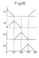
- Fig. 45 is a diagram showing one example of a change in the weight in the phase-combining circuit shown in Fig. 44 .
- the signals (input, phases) F1 to F4 processed by the input signal processing sections 811 to 814 respectively are supplied to the'phase-combining circuit (variable weight interpolator) 802.
- This phase-combining circuit 802 includes pairs of differential transistors 821, 822, 824, 825, 827, 828, 830 and 831 supplied with the signals F1 and F3, F2 and F4, F3 and F1, and F4 and F2 respectively, transistors 823, 826, 829 and 832 supplied with the weights (weight signals) W1, W2, W3 and W4 at their gates respectively, a load device 833 connected in common to the pairs of differential transistors, and an output buffer 834.
- the output buffer 834 is for converting signal levels of a small amplitude at both ends of the load device 833 into output signals of a large amplitude (full CMOS amplitude).
- the output buffer 834 is structured as a supply-insensitive buffer circuit (refer to Fig. 31 ) in which a delay is not easily varied by a power source voltage.
- the structure of the weight signal generator circuit is omitted from Fig. 44 .
- the operation of the phase-combining circuit 802 is similar to that of the phase-combining circuit 5 shown in Fig. 11 .
- the weight signals W1, W2, W3 and W4 are supplied to the gates of the transistors 823, 826, 829 and 832 respectively.
- the present circuit has a small number of signal lines of two sets of differential signals for input signals.
- the input signals of the variable weight interpolator (phase-combining circuit) 802 have high relative phase precision. Further, the variable weight interpolator 802 exhibits excellent linearity, so that it is possible to generate high-precision timing signals.
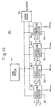
- Fig. 46 is a block circuit diagram schematically showing a timing signal generator circuit to which the operation principle shown in Fig. 42 has been applied.
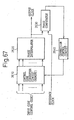
- Fig. 47 is a circuit diagram showing one example of a phase-combining circuit in the timing signal generator circuit shown in Fig. 46 .
- reference numbers 841 to 844 denote weight processing sections.
- the phase-combining circuit 802 in the timing signal generator circuit is constructed of the four weight processing sections 841 to 844 to which the weights W1 to W4 and all the input phases (signals F1 to F4) have been supplied.
- each weight processing section (841) includes p-MOS transistors 8401 to 8404 that structure loads, and n-MOS transistors 8405 to 8413.
- Transistors 8405 and 8406 and transistors 8408 and 8409 constitute pairs of differential transistors respectively for applying weights (w1) based on the signals F1 to F4. These transistors are connected to the load device 833 via transistors 8411 and 8412.
- the four weight processing sections 841 to 844 are provided for the four weights W1 to W4 respectively, and are connected to the load device 833 respectively thereby to combine signals.
- a timing signal is output via the output buffer 834.
- the supply-insensitive buffer circuit 834 is used as the output buffer in a similar manner to that of the circuit shown in Fig. 44 .
- the output of the fixed-weight interpolator (weight processing sections 841 to 844) is directly input to the variable-weight interpolator 802.
- a signal conversion into a CMOS full amplitude level by a comparator is omitted, which makes it possible to achieve a higher-speed signal transmission and a lower power consumption.
- Fig. 48 is a diagram for explaining another operation principle of a timing signal generator circuit.
- Fig. 49 is a block circuit diagram schematically showing a timing signal generator circuit to which the operation principle shown in Fig. 48 has been applied.
- a reference number 901 denotes an input signal processing circuit having six input signal processing sections 911 to 916
- 902 denotes a phase-combining circuit.
- Each of the input signal processing sections 911 to 916 can be structured as an interpolator of an equal weight for three inputs.
- the timing signal generator circuit uses as input signals three sets of differential signals (f1, f4; f2, f5; f3, f6) of which mutual phase difference is near 60 degrees.
- These signals f1 to f6 may be considered as signals of sixth phases.
- two phases with two phases in the middle skipped have a mutual phase difference of 180 degrees.
- the signal f1 and the signal f4 have a mutual phase difference of 180 degrees
- the signal f2 and the signal f5 have a mutual phase difference of 180 degrees.
- the'signal f3 and the signal f6 have a mutual phase difference of 180 degrees.
- a PLL circuit 903 generates a signal that is synchronous with a clock clk that has been supplied from the outside of the chip. Then, the phase of this signal is divided by using DLL sections 961 to 963, a phase detector 904 and a charge pump 905, to produce three sets of differential signals (f1, f4; f2, f5; f3, f6) whose phases are mutually different by 120 degrees. These differential signals are then supplied to an input signal processing circuit 901 via buffers 971 to 973.
- the above input signals (three sets of differential signals f1, f4; f2, f5; f3, f6) are also used for driving other various circuits. Therefore, there is a case where the phase differences are not exactly 120 degrees due to a delay attributable to input capacitance and wiring capacitance of the input circuits. However, based on a complementary change and a coupling of lines for transmitting the differential signals, it is possible to keep the phase difference of each differential signal (differential clock signal) to 180 degrees substantially accurately.
- New signals F1 to F6 are generated as follows in a similar manner to that when the two sets of differential signals (f1, f3; f2, f4) are produced with reference to Fig. 42 . Timing signals are generated by using these signals F1 to F6.
- the input signal processing sections 911 to 916 process the signals F1 to F6 as follows by excluding a constant offset phase due to the phase combining.
- F ⁇ 1 f ⁇ 1 + f ⁇ 2 + f ⁇ 3 / 3
- F ⁇ 2 f ⁇ 2 + f ⁇ 3 + f ⁇ 4 / 3
- F ⁇ 3 f ⁇ 3 + f ⁇ 4 + f ⁇ 5 / 3
- F ⁇ 4 f ⁇ 4 + f ⁇ 5 + f ⁇ 6 / 3
- F ⁇ 5 f ⁇ 5 + f ⁇ 6 + f ⁇ 1 + 2 ⁇ ⁇ / 3
- F ⁇ 6 f ⁇ 6 + f ⁇ 1 + f ⁇ 2 + 4 ⁇ ⁇ / 3
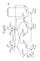
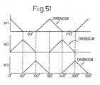
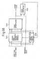
- Fig. 50 is a circuit diagram showing one example of a phase-combining circuit in the timing signal generator circuit shown in Fig. 49 .
- Fig. 51 is a diagram showing one example of a change in the weight in the phase-combining circuit shown in Fig. 50 .
- phase-combining circuit 902 is constructed of switches 921, 922 and 923 for inverting the signals F1, F4, F2, F5, F3 and F6 respectively, pairs of differential transistors 9201, 9202, 9204, 9205, 9207 and 9208 supplied with outputs of these switches 921 to 923 respectively, transistors 9203, 9206 and 9209 supplied with weights (weight signals) W1, W2 and W3 to their gates respectively, a load device 9210 connected in common to each pair of differential transistors, and an output buffer 921.
- the weights W1 to W3 are obtained as outputs of a weight signal generator circuit (D/A converter: 51, 530) that generates a weight from a phase control code, for example.
- these weight signals are generated based on a phase control code consisting of two bits of polarity control signals and four bits of weight control signals, for example.
- the weight W1 is inverted within a range of phases from 90 degrees to 270 degrees
- the weight W2 is inverted within a range of phases from 150 degrees to 330 degrees
- the weight W3 is inverted within a range of phases from 210 degrees to 390 (30) degrees.
- the signals F1, F4, F2, F5, F3 and F6 change over the polarities of differential signals that are input to the pairs of differential transistors by the switches 921, 922 and 923 respectively.
- the currents of the pairs of differential transistors (9201, 9202, 9204, 9205, 9207 and 9208) of which tail currents have been controlled by the weights W1 to W3 are integrated by the load device 9210. Then, zero crosses of differential signals obtained are detected, and a result is output.
- the load device 9210 of the phase-combining circuit 902 has an integration capacity added to the cross-coupled p-MOS load having a differential impedance in high resistance, for example. As explained above, the cross-coupled p-MOS load shows a high impedance for a differential signal but shows a low impedance for an in-phase signal.
- An output buffer (comparator) 9211 is connected to this load device 9210 to convert a signal of a small amplitude into an output signal of a large amplitude. (full CMOS amplitude).
- the output buffer 9211 is a supply-insensitive buffer circuit in which a delay is not much dependent on a power source voltage Vdd.
- the phase-combining circuit shown in Fig. 50 can provide a high-precision timing signal generator circuit in a simple structure based on a small number of input phases.
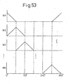
- Fig. 52 is a circuit diagram showing another example of a phase-combining circuit in the timing signal generator circuit shown in Fig. 49 .
- Fig. 53 is a diagram showing one example of a change in the weight in the phase-combining circuit shown in Fig. 52 .
- a phase-combining circuit (variable-weight interpolator) 902 is constructed of pairs of differential transistors 9301, 9302, 9304, 9305, ---, 9316 and 9317 to which signals F1, F4, F2, F5, ---, F6 and F3 have been supplied, transistors 9303, 9306, ---, and 9318 supplied with weights (weight signals) W1, W2, ---, and W6 to their gates respectively, a load device 9210 connected in common to each pair of differential transistors, and an output buffer 9211.
- phase-combining circuit shown in Fig. 52 instead of the inputs of three phases, inputs of six phases are applied.
- the phase-combining circuit shown in Fig. 52 uses a larger number of input phases than the input phases of the phase-combining, circuit shown in Fig. 50 .
- this arrangement does not incur a disturbance of input signals due to the inversion of polarities. As a result, it is possible to generate timing signals in higher precision.
- timing signals in high precision without receiving an influence of phase errors that are generated at the time of a generation and distribution of reference signals.
- phase-combining circuits phase interpolator circuits
- weighted sum generator circuits and comparators are analog circuits, and designing the circuits with high linearity is becoming increasingly difficult with increasing miniaturization in semiconductor processes and attendant reductions in supply voltage. In view of this situation, it is needed to realize a phase-combining circuit or timing signal generator circuit having high linearity without requiring more than necessary linearity in the analog circuits.
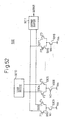
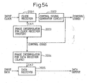
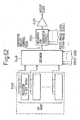
- Fig. 54 is a block diagram showing one example of a system having master and slave phase-combining circuits (phase interpolators).
- reference numeral 2001 is a clock receiver
- 2002 is a control signal generator circuit
- 2003 and 2004 are the phase interpolators
- 2005 is a data receiver.
- the clock receiver 2001 receives a clock signal supplied from the outside, and the control signal generator circuit 2002 outputs a control code (digital control code) in accordance with a signal output from the clock receiver 2001; the control code from the control signal generator circuit 2002 is supplied to control the phase interpolator (master) 2003 for the clock receiver so that the phase of a clock CK1 output from it matches the phase of the clock (input clock) input to the receiver 2001.
- a control code digital control code
- the control code from the control signal generator 2002 is also supplied to the phase interpolator (slave) 2004 for the data receiver, and a clock CK2 is thus supplied to the data receiver 2005.
- a plurality of phase interpolators 2004 for data receivers are provided, for example, for the phase interpolator 2003 for one clock receiver.
- the phase interpolator 2004 for each data receiver generates the clock CK2 and supplies it to the data receiver 2005.
- the slave phase interpolators are not limited to those for the data receivers provided one for each data line, but are also provided for various other circuits that use synchronized clocks.
- Figs. 55 and 56 are diagrams showing one example of a prior art phase-combining circuit.
- phase-combining circuit phase interpolator 2003 (2004) comprises, for example, D/A converters 2340 which output currents (weighting currents) I1 to I4, respectively, in accordance with the control code supplied from the control signal generator circuit 2002, and a four-phase clock generator circuit 2350 which generates four clock signals ⁇ 1 to ⁇ 4 shifted in phase by 90 degrees from one another.
- the currents I1 to I4 from the D/A converters 2340 are made to flow through transistors 2321 to 2324, respectively, and applied as weights W1 to W4 to the gates of the transistors 2303, 2306, 2309, and 2312 respectively connected to differential pairs of transistors (2301, 2302; 2304, 2305; 2307, 2308; and 2310, 2311).
- the transistors in the respective differential pairs (2301, 2302; 2304, 2305; 2307, 2308; and 2310, 2311) are supplied at their gates with clock signals of different phases ( ⁇ 1, ⁇ 3; ⁇ 2, ⁇ 4; ⁇ 3, ⁇ 1; and ⁇ 4, ⁇ 2), and are controlled in accordance with the respective weights W1 to W4, to output the clock CK1 (CK2) via a comparator 2320.
- reference numeral 2330 designates a load.
- the load 2330 is constructed from pMOS transistors 2331 to 2334.
- the phase interpolator shown in Figs. 55 and 56 generates from the four phase clock signals ⁇ 1 to ⁇ 4 a voltage waveform corresponding to the integral of the weighted sum, and generates the desired phase by converting this waveform into a pulse wave by means of the comparator 2320.
- the weights W1 to W4 are generated in accordance with the control code.
- the control code is supplied not only to the master phase interpolator 2003 but also to the slave phase interpolator 2004 to generate the clock.
- phase interpolator In a system having master and slave phase interpolators such as the one shown in Fig. 54 , if there exists a nonlinear relationship between the control code and output phase in the phase interpolators, phase errors induced by this linearity will be introduced in the outputs of the master and slave phase interpolators or in the output of each slave phase interpolator. Each phase interpolator also contains subtle characteristic errors due, for example, to variations in transistor characteristics, etc. and these errors become a problem when the clock frequency is increased to increase the data transfer rate.
- the weighted sum generator circuit and the comparator are analog circuits, and designing'the circuits with high linearity is becoming increasingly difficult with increasing miniaturization in semiconductor processes and attendant reductions in supply voltage. Further, subtle phase shifts are introduced in the signals transferred on the plurality of data lines (signal lines) because of such factors as the length of each signal line and the existence of parasitic capacitors, and this has made it difficult to latch all the data transferred on these signal lines at optimum timing.
- the present invention can realize a phase-combining circuit and timing signal generator circuit having high linearity without requiring more than necessary linearity in the analog circuits.
- the present invention can also individually control the timing of output signals of the phase-combining circuit.
- phase-combining circuit and timing signal generator circuit according to the present invention will be described in detail below with reference to relevant drawings.
- Fig. 57 is a block diagram showing the basic functional configuration of the phase-combining circuit according to the present invention.
- reference numeral 2400 is a control code converter circuit
- 2500 is a weighted sum generator circuit
- 2420 is a comparator.
- the weighted sum generator circuit 2500 shown here corresponds to the circuitry comprising the D/A converter array 2340, load 2330, and transistors 2301 to 2312 and 2321 to 2324 in the phase-combining circuit previously shown in Figs. 55 and 56 .
- a control code (input code) is input to the weighted sum generator circuit 2500 via the control code converter circuit 2400. That is, in the phase-combining circuit of Fig. 57 , the control code converter circuit 2400 is interposed between the input code to the phase interpolator (the output of the control signal generator circuit in Fig. 54 ) and the weighted sum generator circuit 2500 which takes a weighted sum on multiple phase clocks (for example, four phase clocks ⁇ 1 to ⁇ 4).
- the weighted sum generator circuit 2500 is chosen to have a resolution sufficiently higher than a value corresponding to the number of bits in the input code (control code) (so as to provide smaller phase steps).
- Figs. 58A and 58B are diagrams for explaining the operation of the phase-combining circuit shown in Fig. 57 .
- reference character AL indicates an ideal curve (ideal straight line) representing an ideal relationship between the output signal phase of the phase-combining circuit and the control code
- RLo represents a characteristic curve showing the relationship between the output signal phase and the control code in the prior art phase-combining circuit (the configuration without the control code converter circuit 2400).
- reference character RL indicates a characteristic curve (substantially coinciding with the ideal straight line) showing the relationship between the output signal phase and the control code in the phase-combining circuit of Fig. 57 .
- phase-combining circuit timing signal generator circuit
- the linearity of the circuit as a whole can be enhanced by adding a small amount of digital circuitry and without requiring excessive linearity in the analog circuits such as the weighted sum generator circuit (weight generator circuit) and the comparator.
- Figs. 59 and 60 are diagrams showing a first embodiment of a phase-combining circuit according to the arrangement of Fig. 57 .
- reference numerals 2511 to 2514 are current D/A converters which output currents (weighting currents) I1 to I4 in accordance with the converted control code into which the input code (control code) has been converted by the control code converter circuit 2400.
- the weighted sum generator circuit 2500 shown in Fig. 57 corresponds to the circuitry comprising the D/A converters (D/A converter array) 2511 to 2514, load 2430, and transistors 2401 to 2412 and 2421 to 2424 in the phase-combining circuit (phase interpolator) shown in Figs. 59 and 60 .
- phase clock signals ( ⁇ 1, ⁇ 3; ⁇ 2, ⁇ 4; ⁇ 3, ⁇ 1; and ⁇ 4, ⁇ 2) applied to the gates of the respective transistors (2401, 2402; 2404, 2405; 2407, 2408; and 2410, 2411) are generated, for example, by using a PLL and causing them to synchronize with a clock supplied from outside the chip.
- phase clock signals ⁇ 1 to ⁇ 4 are phase shifted, for example, by 90 degrees relative to one another.
- the input code for example, the control code from the control signal generator circuit 2002 in Fig. 54
- the control code converter circuit 2400 so that the relationship between the control code and the output phase becomes linear
- the control code thus converted is supplied to the D/A converters 2511 to 2514.
- the converted weight control code obtained by converting the input code by the control code converter circuit 2400 so that the relationship between the control code and the output phase becomes linear, is input to the D/A converters 2511 to 2514, and the currents (weighting currents) I1 to I4 corresponding to the converted weight control code are output from the respective D/A converters 2511 to 2514.
- the transistors in the respective differential pairs (2401, 2402; 2404, 2405; 2407, 2408; and 2410, 2411) are supplied at their gates with clock signals of different phases ( ⁇ 1, ⁇ 3; ⁇ 2, ⁇ 4; ⁇ 3, ⁇ 1; and ⁇ 4, ⁇ 2), and are controlled in accordance with the respective weights W1 to W4, to output the clock (corresponding to the clock CK1 or CK2 in Fig. 54 ) via the comparator 2420.
- reference numeral 2430 designates a load.
- the load 2430 is constructed from pMOS transistors 2431 to 2434.
- Figs. 61A and 61B are diagrams showing one example of how the weights change in the phase-combining circuit of this embodiment: Fig. 61A shows the change of the weights W1 and W3, and Fig. 61B depicts the change of the weights W2 and W4.
- the weights W1 to W4 (the output currents of the current D/A converters 2511 to 2514) change as shown, for example, in Figs. 61A and 61B .
- ordinate I represents the current
- absc issa ⁇ the output phase of the phase-combining circuit, and the output phase when the weight W1 takes a maximum value Wmax is taken as the origin of the phase.
- each weight Wn (W1 to W4) takes a maximum value Wmax as the highest value and a minimum value Wmin as the lowest value and, at any output phase, takes a nonzero value (a predetermined bias current is included). That is, the weights (currents) W1 to W4 generated by the D/A converters 2511 to 2514 each include a predetermined (Wmin) bias current to ensure stable operation of the transistors to which the weights are applied.
- each weight Wn (W1 to W4) is shown as a triangular wave with its lower half clamped.
- the input code is 6 bits long per cycle
- the converted weight control code is 9 bits long per cycle; that is, the control code converter circuit 2400 generates the 9-bit weight control code from the 6-bit input code.
- the input-output characteristic as a whole can be made linear by choosing the relationship between the input code and the converted weight control code in such a manner as to offset the nonlinearity.
- phase-combining circuit phase interpolator of the first embodiment, when, in each phase interpolator (each slave), the input code (control code) is converted by the control code converter circuit 2400 into the converted weight control code for input to the D/A converters 2511 to 2514 so that the relationship between the input code and the output phase becomes linear, the output (phase) of each slave phase interpolator (2004) can also be made to precisely match the phase of the input clock, as in the case of the master phase interpolator (2003).
- Fig. 62 is a block diagram showing a second embodiment of a phase-combining circuit using the arrangement of Fig. 57 .
- the conversion from the input code to the converted weight control code is performed by a decoder 2440 based on the data stored in a memory (register array) 2450.
- the memory for storing the mapping between the input code and the converted weight control code need only have a capacity as small as 9 bits (for the converted weight control code) ⁇ 2 6 (for 64 words of the input code); therefore, the memory can be constructed as the register array 2450.
- the input code is used as an address to specify the location in the memory at which the corresponding converted weight control code is stored, and the decoder 2440 outputs the data stored at the specified location as the converted weight control code.
- the second embodiment offers the advantage that the mapping between the input code and the output phase (the converted weight control code) can be changed flexibly by altering the contents of the memory. It is also possible to compensate for variations in characteristics due to production processes.
- Fig. 63 is a block diagram showing a third embodiment of a phase-combining circuit according to this aspect of the present invention.
- an up-down signal is input to an up-down counter 2470 and, in accordance with an output of the up-down counter 2470, a decoder 2460 reads the corresponding converted weight control code from the register array 2450 and outputs it for phase control.
- the address to specify the location of the weight control code to be used is incremented or decremented in accordance with the up-down signal, and the converted weight control code stored at the specified location in the register array 2450 is read out of the register array 2450 and, using its value, a weighted sum is generated.
- supplying the up-down signal is preferable to supplying the entire input code (control code), because the number of signal lines used to transfer the up-down signal (control code) can be reduced.
- Fig. 64 is a block diagram showing a control code converter circuit as a fourth embodiment of a phase-combining circuit.
- control code converter circuit 2400 is constructed using a shift register array 2460 in place of the register array 2450 and decoder 2440 in the second embodiment shown in Fig. 62 .
- the control code converter circuit 2400 in the fourth embodiment comprises 64-word shift registers, one for each of the 9 bits, and produces a 9-bit output code (converted weight control code) from a 6-bit input code by shifting the bits to the right or left in accordance with the application of a shift signal (up-down signal).
- the -fourth embodiment offers the advantage that when controlling the phase of each slave phase interpolator provided for each of multi-channel transmission lines, synchronized operation can be performed while maintaining channel-to-channel skew at a proper value.
- Fig. 65 is a diagram showing an output phase versus control code relationship for explaining a fifth embodiment of a phase-combining circuit in this aspect of the present invention.
- the relationship between the converted weight control code corresponding to the input code and the output phase is made as linear as possible within the phase range that the phase interpolator uses. More specifically, in the fifth embodiment, the relationship between the input code and the converted weight control code is chosen so that it becomes linear within the range that the phase interpolator uses (for example, the range of 90 to 270 degrees), not over the entire range of 360 degrees (2 ⁇ ) (the range corresponding to one clock cycle). In this way, when it is known that the range that the phase interpolator uses is limited, a higher resolution can be achieved.
- the fifth embodiment thus offers the advantage of being able to achieve high linearity and high resolution which are usually desirable characteristics.
- Fig. 66 is a circuit diagram showing a phase-combining circuit not in accordance with the invention.
- Fig. 66 includes a current D/A converter (correction D/A converter) 2480 for generating a correction weight, in addition to the regular weight generator circuit (weighted sum generator circuit) provided in the prior art phase-combining circuit. More specifically, outputs of the correction D/A converter 2480 are supplied as inputs to the comparator 2320 to correct for the nonlinearity of the output phase relative to the input code.
- An output (for example, 4 bits) of a correction control code converter circuit 2490 for converting the input code (for example, 6 bits) into a correction control code is supplied as an input to the correction D/A converter 2480.
- the resolution of the current D/A converters (D/A converter array 2340) for generating the weighting currents 11 to I4 from the input code (converted weight control code: 6 bits), for example, is 6 bits as in the prior art example, and there is no need to increase the resolution to 9 bits as in the first embodiment shown in Fig. 59 .
- the D/A converter array (2340) has a current output range sufficient to cover the width of nonlinearity (displacement from the ideal linear relationship) obtained with the normal weight range.
- correction D/A converter 2480 need only perform D/A conversion on the correction code of, for example, 4 bits, into which the input code has been converted by the correction control code converter circuit 2490, and as a result, the circuit configuration as a whole can be simplified.
- the linearity between the input code and the output phase can be enhanced by appropriately selecting the value of the correction weight; furthermore, not only can the amount of circuitry, such as a memory device, be reduced by reducing the number of bits in the correction data, but a more precise correction for nonlinearity can be achieved.
- Fig. 67 is a circuit diagram showing a sixth embodiment of a phase-combining circuit in this aspect of the present invention.
- reference numeral 2610 is a control code converter circuit
- 2620 is a phase interpolator
- 2630 is a phase comparator
- 2640 is a correction control circuit.
- the phase-combining circuit of the sixth embodiment includes the control code converter circuit 2610, phase comparator 2630, and correction control circuit 2640, in addition to the phase interpolator 2620.
- a reference clock is received from the outside, the phase of the output clock is compared in the phase comparator 2630 with the phase of the reference clock, and writing is performed to a memory in the control code converter circuit 2610 via the correction control circuit 2640 (the memory here corresponds, for example, to the register array 2450 in the second embodiment shown in Fig. 62 ).
- the writing to the memory is performed at the initial setting stage, etc., for example, during system power-on.
- the correspondence between the input code and the converted weight control code is corrected using the phase of the externally applied reference clock. That is, to perform the correction, a variable phase reference clock is applied from the outside, and at the same time, a phase-locked loop is formed at the phase interpolator 2620 side with such circuits as the phase comparator 2630 for comparing the phase of the output clock with the phase of the reference clock and the correction control circuit 2640 having a digital filter, etc. for processing the result of the comparison (a digital signal "0" or "1" indicating a phase advance or delay).
- the desired input code is applied from the outside and, at the same time, the reference clock having the desired phase for output is applied; in this condition, the phase-locked loop is operated to adjust the converted weight control code to such a value that makes the output clock match the reference clock, and the values of the input code and the' converted weight control code obtained at this time are written to the memory.
- desired dependency can be obtained over a prescribed phase output range of the output clock (for example, over the entire range of one cycle, i.e., 360 degrees (2 ⁇ )).
- Fig. 68 is a circuit diagram showing a seventh embodiment of a phase-combining circuit of the invention.
- the correction using the reference clock has been performed for all input codes, but in the seventh embodiment, the correction is performed by selecting a limited number of values from the entire set of input codes. More specifically, in the seventh embodiment, the correction using the reference clock is performed only at four points (for example, at 90 degrees, 180 degrees, 270 degrees, and 360 degrees (0 degree)), and for any input code in-between, the correction control circuit 2650 generates the converted weight control code by linear interpolation.
- Figs. 69A and 69B are diagrams for explaining the operation of the phase-combining circuit shown in Fig. 68 .
- reference character AL indicates an ideal curve (ideal straight line) representing an ideal relationship between the output signal phase of the phase-combining circuit and the control code
- RLo represents a characteristic curve showing the relationship between the output signal phase and the control code when the control code conversion is not performed.
- reference character RL indicates a characteristic curve (linearly interpolated) showing the relationship between the output signal phase and the control code in the phase-combining circuit of the seventh embodiment.
- the nonlinearity of a phase interpolator in general can be represented mostly by a gently sloping S-shaped curve, as shown in Fig. 69A , if the converted weight control code is generated by performing the correction using the reference clock for the input codes only at four points, for example, at 90 degrees, 180 degrees, 270 degrees, and 360 degrees (0 degree), and for any input code in-between, the converted weight control code is generated by linear interpolation, a sufficient linear characteristic can be obtained.
- the seventh embodiment offers the advantage of being able to shorten the time required for the correction and to simplify, at the same time, the configuration of the correction signal generator.
- Fig. 70 is a diagram for explaining an eighth embodiment of a phase-combining circuit.
- the eighth embodiment uses a reference clock whose frequency is slightly different from that of a phase interpolator driving clock (for example, clock ⁇ 1 selected from among the four phase clocks ⁇ 1 to ⁇ 4).
- phase difference of one cycle i.e., 360 degrees (2 ⁇ )
- This phase difference is sufficiently trackable by the correction phase-locked loop containing the phase interpolator, and in the range of this number of clock cycles, the two clock phases can be considered to deviate relative to each other linearly over time.
- the value of the converted weight control code that achieves a linear relationship between the input code and the output clock phase can be obtained.
- a phase interpolator can be provided that achieves an input code versus output phase characteristic having highly precise linearity (or any desired dependency) without requiring more than necessary precision in the linearity of the analog circuits such as the weighted sum generator circuit and the comparator.
Landscapes
- Physics & Mathematics (AREA)
- Nonlinear Science (AREA)
- Engineering & Computer Science (AREA)
- Mathematical Physics (AREA)
- Theoretical Computer Science (AREA)
- Computer Networks & Wireless Communication (AREA)
- Signal Processing (AREA)
- Software Systems (AREA)
- Computer Hardware Design (AREA)
- General Physics & Mathematics (AREA)
- Stabilization Of Oscillater, Synchronisation, Frequency Synthesizers (AREA)
- Synchronisation In Digital Transmission Systems (AREA)
Claims (6)
- Circuit de combinaison de phases comprenant :un circuit de conversion de code de commande (2400) conçu pour convertir un premier code de commande numérique qui lui est appliqué en entrée pour générer de cette manière un deuxième code de commande numérique,un circuit de génération de somme pondérée (2500) conçu pour générer des coefficients de pondération conformément audit deuxième code de commande numérique et pour appliquer les coefficients de pondération à une pluralité de signaux d'horloge de phase, qui sont appliqués en entrée au circuit de génération de somme pondérée (2500) pour générer une somme de signaux d'horloge de phase pondérés, etun circuit comparateur (2420) conçu pour convertir la somme générée par le circuit de génération de somme pondérée en un signal d'horloge de sortie,caractérisé en ce que
le circuit de conversion de code de commande (2400) est conçu pour commander la relation entre ledit premier code de commande numérique et la phase dudit signal d'horloge de sortie en ajustant la conversion dudit premier code de commande numérique en ledit deuxième code de commande numérique, qui comprend un plus grand nombre de bits que ledit premier code de commande numérique, de manière à corriger une non-linéarité entre le premier code de commande numérique et la phase du signal d'horloge de sortie. - Circuit de combinaison de phases selon la revendication 1, comprenant en outre un circuit de mémorisation conçu pour mémoriser ledit deuxième code de commande numérique correspondant audit premier code de commande numérique, dans lequel une conversion est exécutée en lisant ledit deuxième code de commande numérique à partir dudit circuit de mémorisation en utilisant ledit premier code de commande numérique en tant qu'adresse.
- Circuit de combinaison de phases selon la revendication 1, comprenant en outre un circuit de mémorisation conçu pour mémoriser ledit deuxième code de commande numérique correspondant audit premier code de commande numérique, dans lequel une conversion est exécutée en lisant ledit deuxième code de commande numérique à partir dudit circuit de mémorisation conformément à un signal montant-descendant en réponse audit premier code de commande numérique.
- Circuit de combinaison de phases selon la revendication 2 ou 3, dans lequel ledit circuit de mémorisation est un réseau de registres ou une mémoire.
- Circuit de combinaison de phases selon la revendication 3, dans lequel ledit circuit de mémorisation est un réseau de registres à décalage, et ledit signal montant-descendant est fourni audit réseau de registres à décalage.
- Circuit de combinaison de phases selon l'une quelconque des revendications 2 à 5, dans lequel ledit circuit de mémorisation a une capacité suffisante pour couvrir le nombre de divisions d'un cycle dudit signal d'horloge de sortie et mémorise ledit deuxième code de commande numérique correspondant audit premier code de commande numérique.
Applications Claiming Priority (7)
| Application Number | Priority Date | Filing Date | Title |
|---|---|---|---|
| JP33632899 | 1999-11-26 | ||
| JP33632899 | 1999-11-26 | ||
| JP2000080792A JP4049511B2 (ja) | 1999-11-26 | 2000-03-22 | 位相合成回路およびタイミング信号発生回路 |
| JP2000080792 | 2000-03-22 | ||
| JP2000312181A JP3880302B2 (ja) | 2000-10-12 | 2000-10-12 | 位相合成回路およびタイミング信号発生回路 |
| JP2000312181 | 2000-10-12 | ||
| EP00310447A EP1104110B1 (fr) | 1999-11-26 | 2000-11-24 | Circuit de combinaison de phase et circuit générateur de signal d'horloge pour transmission de signal à grande vitesse |
Related Parent Applications (1)
| Application Number | Title | Priority Date | Filing Date |
|---|---|---|---|
| EP00310447A Division EP1104110B1 (fr) | 1999-11-26 | 2000-11-24 | Circuit de combinaison de phase et circuit générateur de signal d'horloge pour transmission de signal à grande vitesse |
Publications (2)
| Publication Number | Publication Date |
|---|---|
| EP1538753A1 EP1538753A1 (fr) | 2005-06-08 |
| EP1538753B1 true EP1538753B1 (fr) | 2008-08-20 |
Family
ID=27340775
Family Applications (2)
| Application Number | Title | Priority Date | Filing Date |
|---|---|---|---|
| EP05002166A Expired - Lifetime EP1538753B1 (fr) | 1999-11-26 | 2000-11-24 | Circuit de combinaison de phase et circuit générateur de signal d'horloge pour transmission de signal à grande vitesse |
| EP00310447A Expired - Lifetime EP1104110B1 (fr) | 1999-11-26 | 2000-11-24 | Circuit de combinaison de phase et circuit générateur de signal d'horloge pour transmission de signal à grande vitesse |
Family Applications After (1)
| Application Number | Title | Priority Date | Filing Date |
|---|---|---|---|
| EP00310447A Expired - Lifetime EP1104110B1 (fr) | 1999-11-26 | 2000-11-24 | Circuit de combinaison de phase et circuit générateur de signal d'horloge pour transmission de signal à grande vitesse |
Country Status (5)
| Country | Link |
|---|---|
| US (3) | US20090179674A1 (fr) |
| EP (2) | EP1538753B1 (fr) |
| KR (1) | KR100625705B1 (fr) |
| DE (1) | DE60040026D1 (fr) |
| TW (1) | TW483255B (fr) |
Cited By (1)
| Publication number | Priority date | Publication date | Assignee | Title |
|---|---|---|---|---|
| RU2520350C2 (ru) * | 2011-10-28 | 2014-06-20 | Федеральное государственное унитарное предприятие "Научно-производственное объединение автоматики имени академика Н.А. Семихатова" | Управляющая вычислительная система |
Families Citing this family (84)
| Publication number | Priority date | Publication date | Assignee | Title |
|---|---|---|---|---|
| JP4107847B2 (ja) | 2002-02-01 | 2008-06-25 | 富士通株式会社 | タイミング信号発生回路および受信回路 |
| GB0413149D0 (en) * | 2004-06-12 | 2004-07-14 | Texas Instruments Ltd | Improvements in or relating to interpolation |
| US7298194B2 (en) | 2004-06-12 | 2007-11-20 | Texas Instruments Incorporated | Interpolation |
| GB0413071D0 (en) | 2004-06-12 | 2004-07-14 | Texas Instruments Ltd | Triangulating phase interpolator |
| US7301410B2 (en) * | 2006-03-07 | 2007-11-27 | International Business Machines Corporation | Hybrid current-starved phase-interpolation circuit for voltage-controlled devices |
| EP1855382A1 (fr) | 2006-05-10 | 2007-11-14 | Austriamicrosystems AG | Dispositif et Méthode de détection de la phase |
| KR101297710B1 (ko) * | 2006-08-10 | 2013-08-20 | 삼성전자주식회사 | 낮은 지터 스프레드 스펙트럼 클럭 발생기 |
| US7592846B2 (en) * | 2007-02-16 | 2009-09-22 | Intersil Americas Inc. | Method for using digital PLL in a voltage regulator |
| JP2008262021A (ja) * | 2007-04-12 | 2008-10-30 | Hiromi Murakami | 電気楽器における位相切替装置 |
| KR101287224B1 (ko) | 2009-08-24 | 2013-07-17 | 후지쯔 가부시끼가이샤 | 위상 인터폴레이터 및 반도체 회로 장치 |
| US8294500B1 (en) * | 2009-10-27 | 2012-10-23 | Altera Corporation | Multi-phase interpolators and related methods |
| US9288082B1 (en) | 2010-05-20 | 2016-03-15 | Kandou Labs, S.A. | Circuits for efficient detection of vector signaling codes for chip-to-chip communication using sums of differences |
| US9251873B1 (en) | 2010-05-20 | 2016-02-02 | Kandou Labs, S.A. | Methods and systems for pin-efficient memory controller interface using vector signaling codes for chip-to-chip communications |
| US9985634B2 (en) | 2010-05-20 | 2018-05-29 | Kandou Labs, S.A. | Data-driven voltage regulator |
| US9077386B1 (en) * | 2010-05-20 | 2015-07-07 | Kandou Labs, S.A. | Methods and systems for selection of unions of vector signaling codes for power and pin efficient chip-to-chip communication |
| WO2011148467A1 (fr) | 2010-05-25 | 2011-12-01 | 富士通株式会社 | Interpolateur de phase, circuiterie de réception et dispositif de traitement d'informations |
| KR101727719B1 (ko) * | 2010-10-11 | 2017-04-18 | 삼성전자주식회사 | 위상 보간기 및 그를 포함하는 반도체 장치 및 위상 보간 방법 |
| US9425505B2 (en) | 2010-11-18 | 2016-08-23 | Lattice Semiconductor Corporation | Integrated phase-shifting-and-combining circuitry to support multiple antennas |
| US8451042B2 (en) * | 2011-06-03 | 2013-05-28 | Texas Instruments Incorporated | Apparatus and system of implementation of digital phase interpolator with improved linearity |
| GB2498948A (en) * | 2012-01-31 | 2013-08-07 | Texas Instruments Ltd | A clock phase interpolator with independent quadrant rotation |
| KR101331441B1 (ko) | 2012-06-29 | 2013-11-21 | 포항공과대학교 산학협력단 | 다단 위상믹서 회로 |
| JP6155744B2 (ja) | 2013-03-26 | 2017-07-05 | 富士通株式会社 | クロック位相補間回路およびデータ送受信回路 |
| EP2979388B1 (fr) | 2013-04-16 | 2020-02-12 | Kandou Labs, S.A. | Procédés et systèmes destinés à une interface de communication à large bande passante |
| WO2014210074A1 (fr) | 2013-06-25 | 2014-12-31 | Kandou Labs SA | Signalisation vectorielle à complexité de récepteur réduite |
| EP2849021B1 (fr) * | 2013-09-12 | 2020-01-01 | Socionext Inc. | Circuits et procédés d'alignement de signaux |
| WO2015038867A1 (fr) | 2013-09-16 | 2015-03-19 | Rambus Inc. | Récepteur synchrone de source utilisant une récupération d'horloge à détection de front |
| US9197241B2 (en) * | 2013-12-20 | 2015-11-24 | Nokia Technologies Oy | Output power control for RF digital-to-analog converter |
| JP6340799B2 (ja) | 2014-01-21 | 2018-06-13 | 富士通株式会社 | エンファシス信号生成回路 |
| JP6264056B2 (ja) | 2014-01-22 | 2018-01-24 | 富士通株式会社 | クロックデータリカバリー回路及びその方法 |
| JP6206212B2 (ja) | 2014-01-23 | 2017-10-04 | 富士通株式会社 | タイミング信号発生回路 |
| KR101654639B1 (ko) * | 2014-01-27 | 2016-09-06 | 광주과학기술원 | 믹서 및 믹싱 방법 |
| US9806761B1 (en) | 2014-01-31 | 2017-10-31 | Kandou Labs, S.A. | Methods and systems for reduction of nearest-neighbor crosstalk |
| EP4236217A3 (fr) | 2014-02-02 | 2023-09-13 | Kandou Labs SA | Procédé et appareil pour communications puce à puce de faible puissance à rapport isi contraint |
| KR102240544B1 (ko) | 2014-02-28 | 2021-04-19 | 칸도우 랩스 에스에이 | 클록 임베디드 벡터 시그널링 코드 |
| US9509437B2 (en) | 2014-05-13 | 2016-11-29 | Kandou Labs, S.A. | Vector signaling code with improved noise margin |
| JP6372166B2 (ja) * | 2014-05-27 | 2018-08-15 | 富士通株式会社 | 位相補間器 |
| US9112550B1 (en) | 2014-06-25 | 2015-08-18 | Kandou Labs, SA | Multilevel driver for high speed chip-to-chip communications |
| US9900186B2 (en) | 2014-07-10 | 2018-02-20 | Kandou Labs, S.A. | Vector signaling codes with increased signal to noise characteristics |
| US9432082B2 (en) | 2014-07-17 | 2016-08-30 | Kandou Labs, S.A. | Bus reversable orthogonal differential vector signaling codes |
| WO2016014423A1 (fr) | 2014-07-21 | 2016-01-28 | Kandou Labs S.A. | Transfert de données multipoint |
| KR101949964B1 (ko) | 2014-08-01 | 2019-02-20 | 칸도우 랩스 에스에이 | 임베딩된 클록을 갖는 직교 차동 벡터 시그널링 코드 |
| CN104270124B (zh) * | 2014-09-19 | 2017-03-29 | 中国电子科技集团公司第二十四研究所 | 基于边沿相加的时钟延迟调节电路及其集成芯片 |
| US9160518B1 (en) * | 2014-09-30 | 2015-10-13 | Realtek Semiconductor Corporation | Half-rate clock-data recovery circuit and method thereof |
| US9674014B2 (en) | 2014-10-22 | 2017-06-06 | Kandou Labs, S.A. | Method and apparatus for high speed chip-to-chip communications |
| CN108353053B (zh) | 2015-06-26 | 2021-04-16 | 康杜实验室公司 | 高速通信系统 |
| US10055372B2 (en) | 2015-11-25 | 2018-08-21 | Kandou Labs, S.A. | Orthogonal differential vector signaling codes with embedded clock |
| CN108781060B (zh) | 2016-01-25 | 2023-04-14 | 康杜实验室公司 | 具有增强的高频增益的电压采样驱动器 |
| EP3217558B1 (fr) * | 2016-03-11 | 2020-05-13 | Socionext Inc. | Mesure de différence de temps |
| US10242749B2 (en) | 2016-04-22 | 2019-03-26 | Kandou Labs, S.A. | Calibration apparatus and method for sampler with adjustable high frequency gain |
| US10057049B2 (en) * | 2016-04-22 | 2018-08-21 | Kandou Labs, S.A. | High performance phase locked loop |
| US10003454B2 (en) | 2016-04-22 | 2018-06-19 | Kandou Labs, S.A. | Sampler with low input kickback |
| CN109313622B (zh) | 2016-04-28 | 2022-04-15 | 康杜实验室公司 | 用于密集路由线组的向量信令码 |
| US10153591B2 (en) | 2016-04-28 | 2018-12-11 | Kandou Labs, S.A. | Skew-resistant multi-wire channel |
| WO2017190102A1 (fr) | 2016-04-28 | 2017-11-02 | Kandou Labs, S.A. | Circuit d'attaque multiniveau de faible puissance |
| US10193716B2 (en) | 2016-04-28 | 2019-01-29 | Kandou Labs, S.A. | Clock data recovery with decision feedback equalization |
| TWI632776B (zh) * | 2016-08-18 | 2018-08-11 | 瑞昱半導體股份有限公司 | 相位內插器 |
| US9906358B1 (en) | 2016-08-31 | 2018-02-27 | Kandou Labs, S.A. | Lock detector for phase lock loop |
| CN109831191B (zh) * | 2016-09-13 | 2021-10-26 | 华为技术有限公司 | 一种多路时钟分发电路及电子设备 |
| US10411922B2 (en) | 2016-09-16 | 2019-09-10 | Kandou Labs, S.A. | Data-driven phase detector element for phase locked loops |
| US10200188B2 (en) | 2016-10-21 | 2019-02-05 | Kandou Labs, S.A. | Quadrature and duty cycle error correction in matrix phase lock loop |
| US10200218B2 (en) | 2016-10-24 | 2019-02-05 | Kandou Labs, S.A. | Multi-stage sampler with increased gain |
| US10372665B2 (en) | 2016-10-24 | 2019-08-06 | Kandou Labs, S.A. | Multiphase data receiver with distributed DFE |
| US10128827B1 (en) * | 2016-11-04 | 2018-11-13 | Inphi Corporation | High-speed phase interpolator |
| CN110945830B (zh) | 2017-05-22 | 2022-09-09 | 康杜实验室公司 | 多模式数据驱动型时钟恢复电路 |
| KR102244183B1 (ko) | 2017-05-27 | 2021-04-26 | 유 린 리 | 구동 시스템 |
| US10116468B1 (en) | 2017-06-28 | 2018-10-30 | Kandou Labs, S.A. | Low power chip-to-chip bidirectional communications |
| US10686583B2 (en) | 2017-07-04 | 2020-06-16 | Kandou Labs, S.A. | Method for measuring and correcting multi-wire skew |
| US10203226B1 (en) | 2017-08-11 | 2019-02-12 | Kandou Labs, S.A. | Phase interpolation circuit |
| US10581417B2 (en) | 2017-09-29 | 2020-03-03 | International Business Machines Corporation | Skew sensor with enhanced reliability |
| US10347283B2 (en) | 2017-11-02 | 2019-07-09 | Kandou Labs, S.A. | Clock data recovery in multilane data receiver |
| US10326623B1 (en) | 2017-12-08 | 2019-06-18 | Kandou Labs, S.A. | Methods and systems for providing multi-stage distributed decision feedback equalization |
| US10270456B1 (en) * | 2018-01-02 | 2019-04-23 | Realtek Semiconductor Corp. | Apparatus and method for frequency tripling |
| US10554380B2 (en) | 2018-01-26 | 2020-02-04 | Kandou Labs, S.A. | Dynamically weighted exclusive or gate having weighted output segments for phase detection and phase interpolation |
| CN110446292B (zh) | 2018-05-03 | 2022-07-08 | 李玉麟 | 驱动装置 |
| US11290115B2 (en) | 2018-06-12 | 2022-03-29 | Kandou Labs, S.A. | Low latency combined clock data recovery logic network and charge pump circuit |
| US10630272B1 (en) | 2019-04-08 | 2020-04-21 | Kandou Labs, S.A. | Measurement and correction of multiphase clock duty cycle and skew |
| US10673443B1 (en) | 2019-04-08 | 2020-06-02 | Kandou Labs, S.A. | Multi-ring cross-coupled voltage-controlled oscillator |
| US10958251B2 (en) | 2019-04-08 | 2021-03-23 | Kandou Labs, S.A. | Multiple adjacent slicewise layout of voltage-controlled oscillator |
| KR102403183B1 (ko) * | 2019-05-29 | 2022-05-30 | 한국전자통신연구원 | 디지털 클럭 생성 장치 및 방법 |
| US10715038B1 (en) * | 2019-11-29 | 2020-07-14 | Realtek Semiconductor Corp. | Apparatus and method for frequency quintupling |
| KR20220100182A (ko) * | 2021-01-08 | 2022-07-15 | 삼성전자주식회사 | 글리치 없는 단조 증가 위상 보간기 및 이를 포함하는 통신 장치 |
| US11463092B1 (en) | 2021-04-01 | 2022-10-04 | Kanou Labs Sa | Clock and data recovery lock detection circuit for verifying lock condition in presence of imbalanced early to late vote ratios |
| US11563605B2 (en) | 2021-04-07 | 2023-01-24 | Kandou Labs SA | Horizontal centering of sampling point using multiple vertical voltage measurements |
| US11496282B1 (en) | 2021-06-04 | 2022-11-08 | Kandou Labs, S.A. | Horizontal centering of sampling point using vertical vernier |
Family Cites Families (21)
| Publication number | Priority date | Publication date | Assignee | Title |
|---|---|---|---|---|
| JPS5910621B2 (ja) * | 1975-01-08 | 1984-03-10 | 日本電気株式会社 | デ−タ伝送復調器 |
| US4297641A (en) * | 1979-09-28 | 1981-10-27 | Rca Corporation | Serrodyning system employing an adjustable phase shifting circuit |
| GB2089609A (en) * | 1980-12-12 | 1982-06-23 | Philips Electronic Associated | Clock pulse phase shifter |
| US4868428A (en) * | 1987-02-20 | 1989-09-19 | Cooper J Carl | Apparatus for shifting the frequency of complex signals |
| US4808936A (en) * | 1988-03-25 | 1989-02-28 | Tektronix, Inc. | Continuously variable clock delay circuit |
| US5097141A (en) * | 1990-12-12 | 1992-03-17 | Motorola, Inc. | Simple distance neuron |
| US5157276A (en) * | 1991-09-26 | 1992-10-20 | Tektronix, Inc. | Low jitter clock phase adjust system |
| US5485490A (en) * | 1992-05-28 | 1996-01-16 | Rambus, Inc. | Method and circuitry for clock synchronization |
| US5554945A (en) * | 1994-02-15 | 1996-09-10 | Rambus, Inc. | Voltage controlled phase shifter with unlimited range |
| US5479132A (en) * | 1994-06-06 | 1995-12-26 | Ramtron International Corporation | Noise and glitch suppressing filter with feedback |
| US5541961A (en) * | 1994-08-15 | 1996-07-30 | At&T Corp. | Digitally controlled high resolution hybrid phase synthesizer |
| JP2907053B2 (ja) * | 1995-02-21 | 1999-06-21 | 日本電気株式会社 | スイッチング速度変動検出装置 |
| US5708383A (en) * | 1996-04-26 | 1998-01-13 | Nat Semiconductor Corp | Integrated circuit frequency controlled modulator for use in a phase lock loop |
| US6125157A (en) * | 1997-02-06 | 2000-09-26 | Rambus, Inc. | Delay-locked loop circuitry for clock delay adjustment |
| US5841325A (en) * | 1997-05-12 | 1998-11-24 | Hewlett-Packard Company | Fully-integrated high-speed interleaved voltage-controlled ring oscillator |
| US6247138B1 (en) * | 1997-06-12 | 2001-06-12 | Fujitsu Limited | Timing signal generating circuit, semiconductor integrated circuit device and semiconductor integrated circuit system to which the timing signal generating circuit is applied, and signal transmission system |
| US5877974A (en) * | 1997-08-11 | 1999-03-02 | National Semiconductor Corporation | Folded analog signal multiplier circuit |
| GB9721384D0 (en) * | 1997-10-08 | 1997-12-10 | Phoenix Vlsi Consultants | Phase locked loop |
| US6002279A (en) * | 1997-10-24 | 1999-12-14 | G2 Networks, Inc. | Clock recovery circuit |
| US6330274B1 (en) * | 1998-09-08 | 2001-12-11 | University Of Hawaii | Spread-spectrum continous-time analog correlator and method therefor |
| WO2001001564A1 (fr) * | 1999-06-29 | 2001-01-04 | Mitsubishi Denki Kabushiki Kaisha | Circuit a semiconducteur |
-
2000
- 2000-11-21 TW TW089124680A patent/TW483255B/zh not_active IP Right Cessation
- 2000-11-24 DE DE60040026T patent/DE60040026D1/de not_active Expired - Lifetime
- 2000-11-24 EP EP05002166A patent/EP1538753B1/fr not_active Expired - Lifetime
- 2000-11-24 EP EP00310447A patent/EP1104110B1/fr not_active Expired - Lifetime
- 2000-11-25 KR KR1020000070666A patent/KR100625705B1/ko not_active IP Right Cessation
-
2009
- 2009-02-02 US US12/320,698 patent/US20090179674A1/en not_active Abandoned
-
2011
- 2011-03-24 US US13/064,429 patent/US20110221506A1/en not_active Abandoned
-
2013
- 2013-07-24 US US13/950,182 patent/US20130314142A1/en not_active Abandoned
Cited By (1)
| Publication number | Priority date | Publication date | Assignee | Title |
|---|---|---|---|---|
| RU2520350C2 (ru) * | 2011-10-28 | 2014-06-20 | Федеральное государственное унитарное предприятие "Научно-производственное объединение автоматики имени академика Н.А. Семихатова" | Управляющая вычислительная система |
Also Published As
| Publication number | Publication date |
|---|---|
| EP1104110A2 (fr) | 2001-05-30 |
| EP1538753A1 (fr) | 2005-06-08 |
| EP1104110B1 (fr) | 2011-09-21 |
| US20110221506A1 (en) | 2011-09-15 |
| US20130314142A1 (en) | 2013-11-28 |
| KR20010082556A (ko) | 2001-08-30 |
| US20090179674A1 (en) | 2009-07-16 |
| EP1104110A3 (fr) | 2003-10-08 |
| DE60040026D1 (de) | 2008-10-02 |
| KR100625705B1 (ko) | 2006-09-20 |
| TW483255B (en) | 2002-04-11 |
Similar Documents
| Publication | Publication Date | Title |
|---|---|---|
| EP1538753B1 (fr) | Circuit de combinaison de phase et circuit générateur de signal d'horloge pour transmission de signal à grande vitesse | |
| JP4049511B2 (ja) | 位相合成回路およびタイミング信号発生回路 | |
| KR100399209B1 (ko) | 클럭 제어 회로 및 클럭 제어 방법 | |
| US7443219B2 (en) | Phase interpolation apparatus, systems, and methods | |
| KR100346804B1 (ko) | 타이밍 신호 발생 회로, 반도체 집적회로 장치, 및 반도체 집적회로 시스템 | |
| JP4093961B2 (ja) | 位相ロックループ回路、遅延ロックループ回路、タイミング発生器、半導体試験装置及び半導体集積回路 | |
| EP1810397A1 (fr) | Procede et appareil de synthèse de frequence | |
| KR101995389B1 (ko) | 위상 혼합 회로, 이를 포함하는 반도체 장치 및 반도체 시스템 | |
| JPH11261408A (ja) | 位相インターポレータ、タイミング信号発生回路、および、該タイミング信号発生回路が適用される半導体集積回路装置並びに半導体集積回路システム | |
| JP2005312053A (ja) | 相互結合型の電圧制御発振器 | |
| USRE38482E1 (en) | Delay stage circuitry for a ring oscillator | |
| US6603339B2 (en) | Precision aligned multiple concurrent duty cycles from a programmable duty cycle generator | |
| EP1067690B1 (fr) | Générateur d'horloge à déphasage variable | |
| US7932766B2 (en) | Digitally controlled oscillator with the wide operation range | |
| CN117097330A (zh) | 延迟自校准电路、直接数字频率合成器及延迟自校准方法 | |
| US20070096787A1 (en) | Method for improving the timing resolution of DLL controlled delay lines | |
| JP3880302B2 (ja) | 位相合成回路およびタイミング信号発生回路 | |
| US6577202B1 (en) | Multiple duty cycle tap points for a precise and programmable duty cycle generator | |
| EP1049257B1 (fr) | Circuit de sélection de phase | |
| US5923200A (en) | Phase modulator circuit | |
| JP2004282360A (ja) | 位相制御回路 | |
| JP2005354271A (ja) | 半導体装置、クロック位相調整回路、送信回路及び受信回路。 | |
| US20040135612A1 (en) | Delayed tap signal generating circuit for controlling delay by interpolating two input clocks | |
| WO2010103626A1 (fr) | Circuit de génération d'horloge et circuit de reproduction de signal l'utilisant | |
| US11843388B2 (en) | Can transmitter |
Legal Events
| Date | Code | Title | Description |
|---|---|---|---|
| PUAI | Public reference made under article 153(3) epc to a published international application that has entered the european phase |
Free format text: ORIGINAL CODE: 0009012 |
|
| AC | Divisional application: reference to earlier application |
Ref document number: 1104110 Country of ref document: EP Kind code of ref document: P |
|
| AK | Designated contracting states |
Kind code of ref document: A1 Designated state(s): DE FR GB |
|
| 17P | Request for examination filed |
Effective date: 20051205 |
|
| AKX | Designation fees paid |
Designated state(s): DE FR GB |
|
| 17Q | First examination report despatched |
Effective date: 20060123 |
|
| GRAP | Despatch of communication of intention to grant a patent |
Free format text: ORIGINAL CODE: EPIDOSNIGR1 |
|
| GRAS | Grant fee paid |
Free format text: ORIGINAL CODE: EPIDOSNIGR3 |
|
| GRAA | (expected) grant |
Free format text: ORIGINAL CODE: 0009210 |
|
| AC | Divisional application: reference to earlier application |
Ref document number: 1104110 Country of ref document: EP Kind code of ref document: P |
|
| AK | Designated contracting states |
Kind code of ref document: B1 Designated state(s): DE FR GB |
|
| REG | Reference to a national code |
Ref country code: GB Ref legal event code: FG4D |
|
| REF | Corresponds to: |
Ref document number: 60040026 Country of ref document: DE Date of ref document: 20081002 Kind code of ref document: P |
|
| PLBE | No opposition filed within time limit |
Free format text: ORIGINAL CODE: 0009261 |
|
| STAA | Information on the status of an ep patent application or granted ep patent |
Free format text: STATUS: NO OPPOSITION FILED WITHIN TIME LIMIT |
|
| 26N | No opposition filed |
Effective date: 20090525 |
|
| REG | Reference to a national code |
Ref country code: FR Ref legal event code: PLFP Year of fee payment: 16 |
|
| PGFP | Annual fee paid to national office [announced via postgrant information from national office to epo] |
Ref country code: GB Payment date: 20151118 Year of fee payment: 16 Ref country code: DE Payment date: 20151118 Year of fee payment: 16 |
|
| PGFP | Annual fee paid to national office [announced via postgrant information from national office to epo] |
Ref country code: FR Payment date: 20151008 Year of fee payment: 16 |
|
| REG | Reference to a national code |
Ref country code: DE Ref legal event code: R119 Ref document number: 60040026 Country of ref document: DE |
|
| GBPC | Gb: european patent ceased through non-payment of renewal fee |
Effective date: 20161124 |
|
| REG | Reference to a national code |
Ref country code: FR Ref legal event code: ST Effective date: 20170731 |
|
| PG25 | Lapsed in a contracting state [announced via postgrant information from national office to epo] |
Ref country code: FR Free format text: LAPSE BECAUSE OF NON-PAYMENT OF DUE FEES Effective date: 20161130 |
|
| PG25 | Lapsed in a contracting state [announced via postgrant information from national office to epo] |
Ref country code: DE Free format text: LAPSE BECAUSE OF NON-PAYMENT OF DUE FEES Effective date: 20170601 Ref country code: GB Free format text: LAPSE BECAUSE OF NON-PAYMENT OF DUE FEES Effective date: 20161124 |