EP1536931B1 - Stamping system for manufacturing high tolerance parts - Google Patents
Stamping system for manufacturing high tolerance parts Download PDFInfo
- Publication number
- EP1536931B1 EP1536931B1 EP20030770241 EP03770241A EP1536931B1 EP 1536931 B1 EP1536931 B1 EP 1536931B1 EP 20030770241 EP20030770241 EP 20030770241 EP 03770241 A EP03770241 A EP 03770241A EP 1536931 B1 EP1536931 B1 EP 1536931B1
- Authority
- EP
- European Patent Office
- Prior art keywords
- punch
- die
- stamping
- press
- shaft
- Prior art date
- Legal status (The legal status is an assumption and is not a legal conclusion. Google has not performed a legal analysis and makes no representation as to the accuracy of the status listed.)
- Expired - Lifetime
Links
- 238000004519 manufacturing process Methods 0.000 title description 12
- 238000000034 method Methods 0.000 claims abstract description 43
- 230000008569 process Effects 0.000 claims abstract description 43
- 230000008878 coupling Effects 0.000 claims abstract description 4
- 238000010168 coupling process Methods 0.000 claims abstract description 4
- 238000005859 coupling reaction Methods 0.000 claims abstract description 4
- 125000006850 spacer group Chemical group 0.000 claims description 11
- 239000012530 fluid Substances 0.000 claims description 6
- 238000013519 translation Methods 0.000 claims description 6
- 230000000295 complement effect Effects 0.000 claims description 5
- 238000003754 machining Methods 0.000 claims description 5
- 230000013011 mating Effects 0.000 claims 2
- 230000002401 inhibitory effect Effects 0.000 claims 1
- 230000005693 optoelectronics Effects 0.000 abstract description 18
- 239000013307 optical fiber Substances 0.000 abstract description 10
- 238000005242 forging Methods 0.000 abstract 1
- 239000000835 fiber Substances 0.000 description 66
- 238000013461 design Methods 0.000 description 16
- 239000000463 material Substances 0.000 description 10
- 238000000429 assembly Methods 0.000 description 6
- 230000035515 penetration Effects 0.000 description 5
- 230000000712 assembly Effects 0.000 description 4
- 238000004891 communication Methods 0.000 description 4
- 230000003287 optical effect Effects 0.000 description 4
- 238000003466 welding Methods 0.000 description 4
- 239000010963 304 stainless steel Substances 0.000 description 3
- 229910000589 SAE 304 stainless steel Inorganic materials 0.000 description 3
- 230000009471 action Effects 0.000 description 3
- 238000004458 analytical method Methods 0.000 description 3
- 230000033001 locomotion Effects 0.000 description 3
- 230000004044 response Effects 0.000 description 3
- 238000003324 Six Sigma (6σ) Methods 0.000 description 2
- 238000013459 approach Methods 0.000 description 2
- 238000005452 bending Methods 0.000 description 2
- 238000006243 chemical reaction Methods 0.000 description 2
- 238000005516 engineering process Methods 0.000 description 2
- 238000001228 spectrum Methods 0.000 description 2
- RYGMFSIKBFXOCR-UHFFFAOYSA-N Copper Chemical compound [Cu] RYGMFSIKBFXOCR-UHFFFAOYSA-N 0.000 description 1
- 230000003466 anti-cipated effect Effects 0.000 description 1
- 239000007795 chemical reaction product Substances 0.000 description 1
- 239000011248 coating agent Substances 0.000 description 1
- 238000000576 coating method Methods 0.000 description 1
- 238000010276 construction Methods 0.000 description 1
- 229910052802 copper Inorganic materials 0.000 description 1
- 239000010949 copper Substances 0.000 description 1
- 238000005520 cutting process Methods 0.000 description 1
- 230000007123 defense Effects 0.000 description 1
- 238000006073 displacement reaction Methods 0.000 description 1
- 238000009826 distribution Methods 0.000 description 1
- 238000009957 hemming Methods 0.000 description 1
- 230000002706 hydrostatic effect Effects 0.000 description 1
- 238000002955 isolation Methods 0.000 description 1
- 239000007788 liquid Substances 0.000 description 1
- 230000007246 mechanism Effects 0.000 description 1
- 229910052751 metal Inorganic materials 0.000 description 1
- 239000002184 metal Substances 0.000 description 1
- 238000012544 monitoring process Methods 0.000 description 1
- 238000002360 preparation method Methods 0.000 description 1
- 230000000750 progressive effect Effects 0.000 description 1
- 238000004080 punching Methods 0.000 description 1
- 230000010076 replication Effects 0.000 description 1
- 238000004088 simulation Methods 0.000 description 1
- 230000003746 surface roughness Effects 0.000 description 1
- UONOETXJSWQNOL-UHFFFAOYSA-N tungsten carbide Chemical compound [W+]#[C-] UONOETXJSWQNOL-UHFFFAOYSA-N 0.000 description 1
Images


Classifications
-
- G—PHYSICS
- G02—OPTICS
- G02B—OPTICAL ELEMENTS, SYSTEMS OR APPARATUS
- G02B6/00—Light guides; Structural details of arrangements comprising light guides and other optical elements, e.g. couplings
- G02B6/24—Coupling light guides
- G02B6/36—Mechanical coupling means
- G02B6/38—Mechanical coupling means having fibre to fibre mating means
- G02B6/3807—Dismountable connectors, i.e. comprising plugs
- G02B6/3833—Details of mounting fibres in ferrules; Assembly methods; Manufacture
- G02B6/3855—Details of mounting fibres in ferrules; Assembly methods; Manufacture characterised by the method of anchoring or fixing the fibre within the ferrule
- G02B6/3862—Details of mounting fibres in ferrules; Assembly methods; Manufacture characterised by the method of anchoring or fixing the fibre within the ferrule radially-compressed, longitudinally-split ferrules consisting of a pair of identical matching halves
-
- G—PHYSICS
- G02—OPTICS
- G02B—OPTICAL ELEMENTS, SYSTEMS OR APPARATUS
- G02B6/00—Light guides; Structural details of arrangements comprising light guides and other optical elements, e.g. couplings
-
- B—PERFORMING OPERATIONS; TRANSPORTING
- B21—MECHANICAL METAL-WORKING WITHOUT ESSENTIALLY REMOVING MATERIAL; PUNCHING METAL
- B21D—WORKING OR PROCESSING OF SHEET METAL OR METAL TUBES, RODS OR PROFILES WITHOUT ESSENTIALLY REMOVING MATERIAL; PUNCHING METAL
- B21D28/00—Shaping by press-cutting; Perforating
- B21D28/02—Punching blanks or articles with or without obtaining scrap; Notching
-
- B—PERFORMING OPERATIONS; TRANSPORTING
- B21—MECHANICAL METAL-WORKING WITHOUT ESSENTIALLY REMOVING MATERIAL; PUNCHING METAL
- B21D—WORKING OR PROCESSING OF SHEET METAL OR METAL TUBES, RODS OR PROFILES WITHOUT ESSENTIALLY REMOVING MATERIAL; PUNCHING METAL
- B21D37/00—Tools as parts of machines covered by this subclass
- B21D37/10—Die sets; Pillar guides
- B21D37/12—Particular guiding equipment, e.g. pliers; Special arrangements for interconnection or cooperation of dies
-
- B—PERFORMING OPERATIONS; TRANSPORTING
- B26—HAND CUTTING TOOLS; CUTTING; SEVERING
- B26F—PERFORATING; PUNCHING; CUTTING-OUT; STAMPING-OUT; SEVERING BY MEANS OTHER THAN CUTTING
- B26F1/00—Perforating; Punching; Cutting-out; Stamping-out; Apparatus therefor
- B26F1/38—Cutting-out; Stamping-out
- B26F1/40—Cutting-out; Stamping-out using a press, e.g. of the ram type
-
- G—PHYSICS
- G02—OPTICS
- G02B—OPTICAL ELEMENTS, SYSTEMS OR APPARATUS
- G02B6/00—Light guides; Structural details of arrangements comprising light guides and other optical elements, e.g. couplings
- G02B6/24—Coupling light guides
- G02B6/36—Mechanical coupling means
-
- G—PHYSICS
- G02—OPTICS
- G02B—OPTICAL ELEMENTS, SYSTEMS OR APPARATUS
- G02B6/00—Light guides; Structural details of arrangements comprising light guides and other optical elements, e.g. couplings
- G02B6/24—Coupling light guides
- G02B6/36—Mechanical coupling means
- G02B6/38—Mechanical coupling means having fibre to fibre mating means
- G02B6/3807—Dismountable connectors, i.e. comprising plugs
- G02B6/3833—Details of mounting fibres in ferrules; Assembly methods; Manufacture
- G02B6/3834—Means for centering or aligning the light guide within the ferrule
- G02B6/3838—Means for centering or aligning the light guide within the ferrule using grooves for light guides
- G02B6/3839—Means for centering or aligning the light guide within the ferrule using grooves for light guides for a plurality of light guides
-
- G—PHYSICS
- G02—OPTICS
- G02B—OPTICAL ELEMENTS, SYSTEMS OR APPARATUS
- G02B6/00—Light guides; Structural details of arrangements comprising light guides and other optical elements, e.g. couplings
- G02B6/24—Coupling light guides
- G02B6/36—Mechanical coupling means
- G02B6/38—Mechanical coupling means having fibre to fibre mating means
- G02B6/3807—Dismountable connectors, i.e. comprising plugs
- G02B6/3833—Details of mounting fibres in ferrules; Assembly methods; Manufacture
- G02B6/3855—Details of mounting fibres in ferrules; Assembly methods; Manufacture characterised by the method of anchoring or fixing the fibre within the ferrule
-
- G—PHYSICS
- G02—OPTICS
- G02B—OPTICAL ELEMENTS, SYSTEMS OR APPARATUS
- G02B6/00—Light guides; Structural details of arrangements comprising light guides and other optical elements, e.g. couplings
- G02B6/24—Coupling light guides
- G02B6/36—Mechanical coupling means
- G02B6/38—Mechanical coupling means having fibre to fibre mating means
- G02B6/3807—Dismountable connectors, i.e. comprising plugs
- G02B6/3873—Connectors using guide surfaces for aligning ferrule ends, e.g. tubes, sleeves, V-grooves, rods, pins, balls
- G02B6/3885—Multicore or multichannel optical connectors, i.e. one single ferrule containing more than one fibre, e.g. ribbon type
-
- G—PHYSICS
- G02—OPTICS
- G02B—OPTICAL ELEMENTS, SYSTEMS OR APPARATUS
- G02B6/00—Light guides; Structural details of arrangements comprising light guides and other optical elements, e.g. couplings
- G02B6/24—Coupling light guides
- G02B6/36—Mechanical coupling means
- G02B6/3628—Mechanical coupling means for mounting fibres to supporting carriers
- G02B6/3632—Mechanical coupling means for mounting fibres to supporting carriers characterised by the cross-sectional shape of the mechanical coupling means
- G02B6/3636—Mechanical coupling means for mounting fibres to supporting carriers characterised by the cross-sectional shape of the mechanical coupling means the mechanical coupling means being grooves
-
- G—PHYSICS
- G02—OPTICS
- G02B—OPTICAL ELEMENTS, SYSTEMS OR APPARATUS
- G02B6/00—Light guides; Structural details of arrangements comprising light guides and other optical elements, e.g. couplings
- G02B6/24—Coupling light guides
- G02B6/36—Mechanical coupling means
- G02B6/3628—Mechanical coupling means for mounting fibres to supporting carriers
- G02B6/3648—Supporting carriers of a microbench type, i.e. with micromachined additional mechanical structures
- G02B6/3652—Supporting carriers of a microbench type, i.e. with micromachined additional mechanical structures the additional structures being prepositioning mounting areas, allowing only movement in one dimension, e.g. grooves, trenches or vias in the microbench surface, i.e. self aligning supporting carriers
-
- G—PHYSICS
- G02—OPTICS
- G02B—OPTICAL ELEMENTS, SYSTEMS OR APPARATUS
- G02B6/00—Light guides; Structural details of arrangements comprising light guides and other optical elements, e.g. couplings
- G02B6/24—Coupling light guides
- G02B6/36—Mechanical coupling means
- G02B6/38—Mechanical coupling means having fibre to fibre mating means
- G02B6/3807—Dismountable connectors, i.e. comprising plugs
- G02B6/3873—Connectors using guide surfaces for aligning ferrule ends, e.g. tubes, sleeves, V-grooves, rods, pins, balls
- G02B6/3874—Connectors using guide surfaces for aligning ferrule ends, e.g. tubes, sleeves, V-grooves, rods, pins, balls using tubes, sleeves to align ferrules
- G02B6/3877—Split sleeves
-
- Y—GENERAL TAGGING OF NEW TECHNOLOGICAL DEVELOPMENTS; GENERAL TAGGING OF CROSS-SECTIONAL TECHNOLOGIES SPANNING OVER SEVERAL SECTIONS OF THE IPC; TECHNICAL SUBJECTS COVERED BY FORMER USPC CROSS-REFERENCE ART COLLECTIONS [XRACs] AND DIGESTS
- Y10—TECHNICAL SUBJECTS COVERED BY FORMER USPC
- Y10T—TECHNICAL SUBJECTS COVERED BY FORMER US CLASSIFICATION
- Y10T83/00—Cutting
- Y10T83/444—Tool engages work during dwell of intermittent workfeed
- Y10T83/463—Work-feed element contacts and moves with work
- Y10T83/4635—Comprises element entering aperture in, or engaging abutment surface on, work
-
- Y—GENERAL TAGGING OF NEW TECHNOLOGICAL DEVELOPMENTS; GENERAL TAGGING OF CROSS-SECTIONAL TECHNOLOGIES SPANNING OVER SEVERAL SECTIONS OF THE IPC; TECHNICAL SUBJECTS COVERED BY FORMER USPC CROSS-REFERENCE ART COLLECTIONS [XRACs] AND DIGESTS
- Y10—TECHNICAL SUBJECTS COVERED BY FORMER USPC
- Y10T—TECHNICAL SUBJECTS COVERED BY FORMER US CLASSIFICATION
- Y10T83/00—Cutting
- Y10T83/869—Means to drive or to guide tool
- Y10T83/8821—With simple rectilinear reciprocating motion only
- Y10T83/8855—With spaced guide pins [e.g., die set leader pins]
-
- Y—GENERAL TAGGING OF NEW TECHNOLOGICAL DEVELOPMENTS; GENERAL TAGGING OF CROSS-SECTIONAL TECHNOLOGIES SPANNING OVER SEVERAL SECTIONS OF THE IPC; TECHNICAL SUBJECTS COVERED BY FORMER USPC CROSS-REFERENCE ART COLLECTIONS [XRACs] AND DIGESTS
- Y10—TECHNICAL SUBJECTS COVERED BY FORMER USPC
- Y10T—TECHNICAL SUBJECTS COVERED BY FORMER US CLASSIFICATION
- Y10T83/00—Cutting
- Y10T83/929—Tool or tool with support
- Y10T83/9411—Cutting couple type
- Y10T83/9423—Punching tool
-
- Y—GENERAL TAGGING OF NEW TECHNOLOGICAL DEVELOPMENTS; GENERAL TAGGING OF CROSS-SECTIONAL TECHNOLOGIES SPANNING OVER SEVERAL SECTIONS OF THE IPC; TECHNICAL SUBJECTS COVERED BY FORMER USPC CROSS-REFERENCE ART COLLECTIONS [XRACs] AND DIGESTS
- Y10—TECHNICAL SUBJECTS COVERED BY FORMER USPC
- Y10T—TECHNICAL SUBJECTS COVERED BY FORMER US CLASSIFICATION
- Y10T83/00—Cutting
- Y10T83/929—Tool or tool with support
- Y10T83/9457—Joint or connection
- Y10T83/9473—For rectilinearly reciprocating tool
- Y10T83/9476—Tool is single element with continuous cutting edge [e.g., punch, etc.]
Definitions
- the present invention relates to stamping system and processes, and more particularly stamping processes for manufacturing parts with high tolerances for various applications, such as optical fiber connection.
- Optical fiber based communication channels are the system of choice in many defense and commercial applications because of their high performance and small size.
- fiber optics have "proved-in" in long distance applications, such as city-to-city and continent-to-continent communication spans, because of the lower cost of electrical-to-optical-to-electrical (E-O-E) conversion components, fiber amplifiers, and fiber cables relative to pure electrical systems using coaxial copper cable that do not requiring E-O-E.
- E-O-E electrical-to-optical-to-electrical
- VSR very short reach
- a significant element of the cost of both active and passive fiber components and connectorised cable is the fiber connector itself.
- Precision ferrules and associated means for aligning them e.g., precision split sleeve for single fiber connection, precision ground pins for multi-fiber connections
- the alignment components are normally required to align fibers to active and passive devices, as well as to align two fibers for demountable connection.
- Precision alignment of two polished fiber ends is needed to ensure that overall optical loss in a fiber link is equal or less than the specified optical connector loss budget for a system. For single-mode telecommunication-grade fiber, this typically corresponds to connector fiber alignment tolerances that are less than 1000nm.
- Current connectors have not changed in basic design for more than 20 years, and it is generally accepted that they cost too much and are too difficult to assemble. The cost of manufacturing precision fiber connectors must decrease if fiber optic is to be the communication media of choice for short haul and VSR applications.
- Connectors, in both parallel fiber and single fiber links, operating at multi-gigabit rates must be assembled with subcomponents fabricated with sub micron precision. As if producing parts with such precision levels were not challenging enough, for the resulting end product to be economical it must be done in a fully automated, very high-speed process.
- stamping processes have been deployed in manufacturing processes for mass-producing parts at low cost. However, heretofore, stamping processes have not been effective in producing parts with acceptable tolerances for optoelectronic components. In fact, there is no acceptable high-speed commercial production process that produces optoelectronic components. In fact, there is no acceptable high-speed commercial production process that produces optoelectronic components with acceptable tolerances for optoelectronic components. In fact, there is no acceptable high-speed commercial production process that produces optoelectronic components with acceptable tolerances. U.S Patent Number 4,458,985 to Balliet et al. is directed to an optical fiber connector.
- Balliet describes in a cursory manner that some of the connector components can be produced by a coining or stamping process (e.g., col. 3, lines 20-21, 55-57). However, Balliet does not provide an enabling disclosure of such stamping process, let alone an enabling disclosure of a stamping process for producing parts within 1000nm.
- US6122952 discloses a forming press capable of performing multiple actuations within a single forming process. In this case, the shaft and the punch are in contact, with intermediate moving parts.
- the present invention is directed to a stamping system and process for producing parts having tolerances below 1000nm.
- the invention is particularly suited for producing optoelectronic parts, including, but not limited to, components, assemblies and subassemblies, and passive and active components.
- the system includes one or a progression of stamping stations for supporting a punch or die.
- the stamping stations include a novel structure for guiding the punch in substantial alignment with the die with tight tolerances.
- the system includes a press for providing the stamping stations with the necessary force to perform the particular stamping operation.
- the system is designed to minimize the number of moving components involved in the support structure in guiding the punch to the die.
- the stamping station includes no moving component in the support structure in guiding the punch to the die.
- the stamping station includes a stationary punch holder structure having a shaft sized and shaped to receive the punch with tight tolerances. The punch is guided to the die by sliding through the shaft.
- the system in another aspect of the present invention, includes a locating sub-plate having indexing features for precisely aligning the progression of stamping stations relative to each other.
- the locating sub-plate and its indexing features have exacting tolerances and sub-micron surface finishes.
- the system includes an interface system for coupling the force of the press with the punch but structurally decoupling the press from the punch.
- the interface system also allows isolation of each stamping station so that operation at one station does not affect operation at another station.
- the system includes a ball and socket arrangement, which allows the press to mechanically couple the force to the punch, but structurally decouple from the punch.
- the system includes a hydraulic interface system. Hydraulic fluid mechanically couples the press to the punch and delivers a uniform force to the punch but structurally decouple the press from the punch.
- the system includes a combination of the ball and socket arrangement with hydraulic actuation of the punch.
- Hydraulic actuation allows for structural decoupling of the press from the punch while the ball and socket arrangement facilitates reducing structural stress on the stamping station components.
- the inaccuracies of the press do not influence the ultra-precision of the stamping stations and tooling.
- the present invention is directed to a stamping system and process for manufacturing parts having tolerances below 1,000 nanometers (nm).
- the inventive system and process is particularly suited for producing optoelectronic parts, including, but not limited to, optoelectronic components, assemblies and sub-assemblies, and active and passive components.
- optoelectronic parts including, but not limited to, optoelectronic components, assemblies and sub-assemblies, and active and passive components.
- the present invention is described by reference to embodiments directed to stamping processes for manufacturing optoelectronic components, in particular optical fiber connectors, such as ferrules and split sleeves.
- Stamping is a fabrication process that presses a work piece, such as a metal strip, between a die set assembly into a predetermined shape or pattern. Stamping presses and stamping dies are tools used in the stamping process.
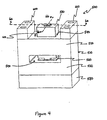
- Figure 1 is a schematic drawing illustrating a conventional stamping press 10.
- the stamping press 10 includes a press ram 20 and a press bed 30.
- the press ram 20 provides the necessary force to stamp a work piece by moving the components of the die set assembly relative to each other.
- the arrow shows the stroke action of the press ram 20 moving up and down relative to the press bed 30.
- the press ram can have other stroke action directions (not shown).
- a die set assembly 40 located between the press ram 20 and the press bed 30, is the tooling used to produce the stamped parts.
- the die set assembly 40 includes a punch 50, structurally coupled to the press ram 20, and a complementary die 60, attached to the press bed 30, or vice-versa.
- the stamping press 10 can include a bolster plate 65 attached to the top of the press bed 30 for attaching the die 60 to the press bed 30.
- the punch 50 and die 60 are aligned with each other such that as the press ram 20 moves towards the press bed 30, the punch 50 and die 60 work in a complementary fashion to implement a desired operation in the work piece.
- a work piece 70 is positioned between the punch 50 and die 60.
- the press ram 20 moves the punch 50 towards the die 60.
- the punch is guided to the die by guideposts and bushings (not shown) and the press ram 20.
- the die set assembly can perform various operations on the work piece, such as cutting and forming operations like punching, drawing, bending, flanging and hemming.
- U.S. Patent No. 6,311,597 B1 discloses a complex stamping system design using a stripper, as a guidepost, and a die nest as a guide bushing.
- the die bushing indirectly guides a punch to a die via directly guiding a punch assembly supporting the punch.
- the punch assembly comprises the punch mounted to a punch shoe, and a stripper guidepost, having a ball bearing cage, mounted to the punch shoe.
- the die nest guides the stripper guidepost, and therefore indirectly guides the punch.
- This complex design is prone to misalignment of the punch and die.
- the punch In order for the punch to be in alignment with the die, it is critical for the punch to be mounted in alignment to the punch shoe and for the stripper to be mounted in alignment to the punch shoe. Any misalignment in assembling any of these components will result in misalignment of the punch and die.
- this design employs at least one moving component in guiding the punch to the die, which can increase the potential for misalignment
- the punch assembly moves within the die nest to guide the punch to the die. Any slight off-center movement of the punch assembly within the die nest will result in misalignment of the punch relative to the die.
- the ball bearing cage By using the ball bearing cage in the design, the potential for misalignment is further compounded. By its very nature, the ball bearings permit off-center movement of the stripper within the die nest, resulting in potential misalignment of the punch and die.
- the stamping system and process of the present invention is capable of producing parts with a "six sigma" geometrical tolerance band of 1,000 nm. Statistically, this means that at most only 3.4 parts per million will not meet dimensional requirements defined by the 1,000 nm tolerance band.
- FIG. 2 is a schematic drawing illustrating a system 100 for stamping optoelectronic components having tolerances below 1,000 nm in accordance with one embodiment of the present invention.
- the stamping system 100 includes means for in-line machining stock material 150, a stamping press 200, one or a progression of stamping stations 250, and a stamping station locating subplate 300.
- the stamping system 100 can include means 150 for in-line machining of stock material 110 into work pieces having predetermined dimensions and surface quality.
- means 150 for in-line machining of stock material 110 into work pieces having predetermined dimensions and surface quality For example, Moore Nanotechnology Systems has developed machine tools employing liquid cooled, oil hydrostatic bearings that have a programming resolution of 10 nm, motion accuracy of 50 nm and feedback resolution of 8.6 nm. These machine tools can be adapted to in-line machine the stock material 110 as it is dispensed from the un-coiler prior to it entering the stamping stations 250. This assures that when the stock material or work piece enters the stamping stations 250 it will be registered in each stamping station with the sub-micron precision necessary to produce optoelectronic components having tolerances below 1,000 nm.
- the stamping system 100 includes the stamping press or a custom-made high-speed energy source 200 for powering the stamping stations 250.
- the stamping press 200 can be any conventional stamping presses well known in the art (e.g. hydraulic, electro-mechanical, etc...), which can support and provide the stamping stations 250 with the necessary force to perform the particular stamping operation.
- the stamping press 200 includes a press ram 210 and a press bed 220. As discussed more fully below, the stamping stations 250 are located between the press ram 210 and the press bed 220.
- the press bed 220 supports the stamping stations 250, and the press ram 210 delivers the necessary force to the stamping stations 250 to perform the stamping operations. It is well known that stamping presses can have stroke actions at speeds in excess of 1,000 strokes per minute (SPM). Additionally, the stamping system can include more than one stamping press to power the stamping stations.
- FIG 3a is a perspective view of a stamping station 400 in accordance with one embodiment of the present invention.
- Figure 3b is a sectional view of the stamping station taken along line 3b-3b shown in Figure 3a .
- the stamping station 400 includes structure for supporting the die set assembly and for directly guiding the punch to the die.
- the stamping station 400 includes a stationary punch holder plate 410, for supporting a punch 420, and a die holder plate 440, for supporting a die 450.
- the punch holder plate 410 functions to align and directly guide the punch 420 to the die 450.
- the punch holder plate 410 has a shaft 430 sized and shaped to slidably receive the punch 420 and to guide the punch 420 to the die 450.
- the shaft 430 allows the punch 420 to translate and penetrate through the punch holder plate 410, in slidable contact with the shaft 430.
- the shaft 430 aligns the punch 420 with the die 450, guiding the punch 420 to a work piece 455 and the die 450.
- the die holder plate 440 also facilitates aligning the die 450 with the punch 420.
- the die 450 is fixedly aligned on the die holder plate 440 in a manner whereby as the punch 420 penetrates through the shaft 430 towards the die holder plate 440 the punch 420 approaches the die 450 in a complementary fashion to operate on the work piece 455.
- a workspace 460 is defined between the punch and die holder plates 410 and 440 by providing spacers 470 between the plates 410 and 440.
- the workspace 460 is an area where the stamping operations occur.
- the work piece 455 is inserted into the workspace 460 where it is stamped to perform a desired operation on the work piece 455; e.g., to form a desired shape of a part.
- the workspace 460 is of sufficient area to accommodate the punch 420 and the die 450, the work piece, and the final stamped part.
- the dimensions of the spacers 470 can be varied, particularly the thickness of the spacers 470, so that the desired dimensions of the workspace 460 can be provided.
- the stamping station 400 includes a stop block 480 for providing a safety stop for the press ram 210 (shown in Figure 2 ).
- the stop block 480 is disposed between the press ram 210 and the top surface of the punch holder plate 410. As the press ram 210 actuates towards the station 400, the stop block 480 contacts with the press ram 210 to inhibit further penetration of the punch 420 into the stamping station 400.
- the stop block 480 controls the depth of penetration of the punch 420 into the stamping station 400. The penetration depth can be controlled by varying the thickness of the stop block 480.
- the stop block 480 can be made from any material of sufficient hardness to withstand repeated impact force from the press ram 210.
- the stop block 480 can have any configuration that will allow the stop block 480 to control the depth of penetration of the punch 420.
- the punch 420 can be coupled to springs 490 or other biasing means for returning the punch 420 to the open position. As the punch 420 is moved towards the die 450, the springs 490 bias. Once the force of the press ram 210 is removed, the springs 490 move the punch 420 away from the die 450.
- the punch holder plate 410 is mounted on the die holder plate 440, with the spacers 470 positioned between the plates 410 and 440.
- the stop block 480 is then mounted on the top surface of the punch holder plate 410.
- Fasteners well known in the art can be used to fasten the components of the stamping station 400 together.
- bores 485 can be provided to receive bolts (not shown) to fasten the components of the stamping station 400 together. When fastened together, the components of the stamping station 400 assemble into a unitary structure.
- FIG 4 is a perspective view of a stamping station 500 in accordance with another embodiment of the present invention.
- Figure 5 is an assembly view of the stamping station 500 shown in Figure 4 .
- Figures 6a and 6b are sectional views of the stamping station 500 shown in Figure 4 , taken along lines 6a-6a and 6b-6b respectively.
- the stamping station 500 includes a stationary, monolithic die set assembly holder structure 510 for supporting the die set assembly.
- the die set holder 510 includes a punch holder section 520 for supporting and guiding a punch 530.
- the punch holder section 520 has a shaft 540 sized and shaped to slidably receive and support the punch 530.
- the shaft 540 is shown in Figure 6 .
- the shaft 540 allows the punch 530 to translate and penetrate through the die set holder 510.
- the punch 530 slides in contact within the shaft 540.
- the shaft 540 facilitates aligning the punch 530 relative to the die, guiding the punch 530 to a work piece 595 (shown in Figure 5 ) and the die.
- the die set holder 510 also includes a die holder section 550 for supporting a die 560.
- the die 560 includes die inserts 562, 563 and 564.
- the die inserts 563 and 564 nest within pockets 565 and 566, respectively.
- the die holder section 550 includes a pocket 570 (shown in Figures 6a and 6b ) for nesting the die 560.
- the pocket 570 is sized and shaped to precisely receive and nest the die 560.
- a backup plate 580 is provided to secure the die 560 within the pocket 570. Once the die 560 is nested within the pocket 570, the backup plate 580 is secured to the bottom of the die set holder 510 to secure the die 560 within the pocket 570.
- the die 560 is fixedly aligned in the die holder section 550 in a manner whereby as the punch 530 penetrates through the shaft 540 towards the die 560, the punch 530 approaches the die 560 in a complementary fashion to operate on the work piece 595.
- a workspace 590 is defined between the punch and die holder sections 520 and 550.
- the workspace 590 is an area where stamping operations occur.
- the work piece 595 is inserted into the workspace 590 where it is stamped to perform a desired operation on the work piece 595.
- the workspace 590 is of sufficient area to accommodate the punch 530 and the die 560, the work piece 595, and the final stamped part (not shown).
- the stamping station 500 includes a stop block 600 for providing a safety stop for the press ram 210 (shown in Figure 2 ).
- the stop block 600 is located between the press ram 210 and the top surface of the die set holder 510.
- the stop block 600 controls the depth of penetration of the punch 530 into the stamping station 500.
- the punch 530 can be coupled to springs 610 or other biasing means for returning the punch 530 to an open position. As the punch 530 is moved towards the die 560, the springs 610 bias. Once the force of the press ram 210 is removed, the springs 610 move the punch 530 away from the die 560.
- the stamping station 500 also includes an ejector 612 for ejecting the stamped part 595 from the die 560 after a stamping operation.
- the ejector 612 includes a lifter 614 and a spring 616 or other biasing means. As discussed more fully below, the ejector 612 is disposed within a hollowed portion of the die insert 562 such that the lifter 614 is capable of engaging the stamped part 595 through the hollowed out portion of the die insert 562.
- the punch and die holder plates 410 and 440 are assembled together to form a unitary structure for supporting the punch 420 and die 450.
- the structures for supporting the punch 530 and die 560 are provided as a monolithic structure.
- the die set holder 510 becomes a more rigid and stable structure, which allows the die set holder 510 to more accurately guide the punch 530 to the die 560.
- FIG 8a is a schematic view of a stamping station 800 in accordance with another embodiment of the present invention.
- the stamping station 800 includes a die holder plate 850, for supporting a die 840, and a shaft 810 for supporting and guiding a punch 860 to the die 840.
- the shaft 810 is sized and shaped to slidably receive and support the punch 860, allowing the punch 860 to translate longitudinally through the shaft 810 towards and away from the die 840.
- the shaft 810 facilitates alignment of the punch 860 with the die 840, guiding the punch 860 to the die 840.
- Adjustable mechanical stoppers 880 are located in the stroke path of the punch 860 for limiting the translation of the punch 860 towards the die 840.
- the punch 860 is provided with a catch 830 which can engage the stoppers 880 to limit further translation of the punch 860 towards the die 840.
- a spacer 895 is provided for adjusting the position of the mechanical stoppers 880 relative to the catch 830.
- the spacer 895 can be angle wedges and screws for micrometric adjustment of the spacers 895.
- the stamping system 100 includes an interface system 700 that mechanically interfaces the force from the press 200 to the stamping station 250 (substantially shown in Figure 2 ), but structurally decoupling the press 200 from the stamping station 250.
- Figure 7a is a simplified drawing of the interface system 700 incorporated in the stamping system 100 of the present invention.
- the stamping press 200 is capable of delivering the necessary force to the stamping station 250 for the stamping operations.
- the force is delivered to the stamping station 250 via the interface system 700.
- the interface system 700 is a ball and socket arrangement.
- a punch 710 is provided with a ball 720
- the press ram 210 is provided with a ball socket 730.
- an adapter plate (not shown), attachable to the press ram 210, can be provided with the ball socket.
- the ball 720 engages the ball socket 730.
- Figure 7b illustrates the ball 720 engaged with the socket 730.
- the interface system 700 facilitates interfacing the force from the stamping press 200 to the stamping station 250.
- the interface system 700 also allows the stamping station 250 to be structurally decoupled from the stamping press 200. None of the stamping station 250 components are directly fixed or bolted to the press ram 210 in any way, thus not being affected by the relative inaccuracies of the press 200. Conventional stamping presses are by nature not built with tight tolerances.
- the press 200 By structurally decoupling the press 200 from the stamping stations 250, the dimensional variability of the press 200 is isolated from the ultra-precise stamping stations 250 and the die set assembly inserts.
- the press 200 can be simply a high speed, repeatable source of energy configured with relatively loose tolerances delivering forces to the ultra precise tools and dies at the stamping stations 250. It should be known to one skilled in the art that the ball and socket arrangement can be reversed, such that the punch is provided with the socket joint and the press ram is provided with the ball joint.
- the system 100 can include a hydraulic interface system for interfacing the force of the press with the stamping station 800.
- the interface system includes an actuator plate 820 disposed within the shaft 810, at an end between the press ram and the punch holder plate.
- the actuator plate 820 is also capable of translating longitudinally within the shaft.
- the shaft 810 is provided with a valve 870 located between the actuator plate 820 and the punch holder plate 830 for providing the shaft 810 with low-pressure hydraulic fluid.
- the shaft 810 is supplied with low-pressure hydraulic fluid via the valve 870.
- the press ram 210 pushes on the actuator plate 820 through the shaft 810 until the actuator plate 820 closes the valve 870.
- the fluid pressure in the shaft 810 increases to exert a force on the punch holder plate 830 to move the punch holder plate 830 and the punch 860.
- the force on the punch holder plate 830 is substantially uniform.
- the force vector is unidirectionally orthogonal to the face of the punch holder plate.
- the hydraulic interface system can also include a ball and socket arrangement.
- Figure 8b is a schematic view of the hydraulic interface system incorporating a ball and socket arrangement.
- the actuator plate 820 can be provided with a ball 920 and the press ram 210 can be provided with a socket 930, or vice versa.
- the press ram 210 engages the actuator plate 820
- the ball 920 engages the socket 930.
- Hydraulic actuation allows the direction of the force applied to the punch 860 to be independent from the direction of the force exerted by the press ram 210.
- the ball 920 and socket 930 arrangement reduces deformation introduced in the structure that holds the hydraulic mechanism, such as the actuator plate 820, and the punch 210 by shear and bending forces resulting from press misalignments.
- the interface system facilitates interfacing the force from the stamping press 200 to the stamping station.
- the interface system also allows the stamping station to be structurally decoupled from the stamping press 200.
- Springs 910 coupled to the punch holder plate 830 can return the punch holder plate 830 away from the die 840.
- Figure 9a is a perspective view of the punch 530 and the die 560 shown in Figures 4 and 5 .
- the punch 530 and die 560 are comprised of blocks with formed surfaces, dowels, punches, cams, sensors and other items. These stamping tools are designed and built with tolerances below 500 nm. This allows the punch 530 and die 560 to be precisely located in the stamping stations 250.
- the punch 530and the die 560 can be designed to be interchangeable between stamping stations.
- Figure 9b is an exploded view of the punch 530 and the die 560 shown in Figure 9a .
- the die 560 includes the die inserts 562, 563 and 564 (the die inserts 563 and 564 are not shown to scale).
- FIG. 9c is a sectional view of the die 560 taken along line 9c-9c of Figure 9a .
- the die 560 includes a formed surface 1020 and a hollowed-out portion 1030 defining an opening 1025 to the formed surface 1020.
- the lifter 614 and the spring 616 are disposed within the hollowed-out portion 1030. If the stamped part (not shown) is still attached to the die 560 after the stamping operation, the lifter 614 and the spring 616 are capable of ejecting the stamped part from the formed surface 1020.
- the lifter 614 is capable of engaging the stamped part through the opening 1025.
- the stamping system 100 is capable of supporting a progression of stamping stations 250.
- Figure 2 shows the system 100 supporting three stamping stations, 260, 261 and 262.
- the progression of stamping stations 250 functions like a conventional progressive die, whereby each of the stamping stations 260, 261 and 263 performs a specific stamping operation.
- the progression of stamping stations 250 allows the system 100 to produce multiple features in the manufactured part simultaneously for every stroke of the punch press 200.
- the system 100 includes a locating subplate 300 disposed on the press bed 220 for precisely aligning the stamping stations 250 relative to each other.
- Figure 16 is a top view of the locating subplate 300 incorporated in the present invention.
- the locating subplate 300 is provided with indexing features 310 for locating the stamping stations 250 relative to each other with sub-micron precision.
- the indexing features 310 can be precisely machined grooves or slots 320 on one of the sub-plate surfaces.
- the grooves 320 are precisely sized and shaped to receive the base of the stamping stations 250. Once the stamping stations 250 are positioned within the grooves 320, the subplate 300 precisely locates the stamping stations 250 relative to each other with sub-micron precision. More than one locating subplate aligned with each other can be utilized depending upon the particular requirements of the application.
- the subplate, or if required, plates, 300 and its indexing features 310 can be fabricated using a precision machine tool, like for example the FV-500 manufactured by Moore Nanotechnology Systems, that can machine the subplate 300 flat and parallel with a surface finish of 10 nm of less.
- the system 100 can include an active feedback controller 350 for continuously monitoring and adjusting various system 100 parameters.
- the controller 350 can be configured to monitor and adjust the amount of force delivered to the stamping station 800 shown in Figure 8a .
- a working pressure relief valve 890 is provided for controlling the amount of force produced, and a stop pressure relief valve 900 is provided to minimize damage to the stamping station 800.
- the working pressure relief valve 890 can be a low flow valve with good accuracy on the pressure setting.
- the stop pressure relief valve 900 can be a high flow valve with a closing histeresis, and is set to a significantly higher pressure than the pressure of the valve 890.
- the working pressure relief valve 890 and the stop pressure relief valve 900 can be a mechanical or electromechanical-type valve for faster response time.
- the controller 350 can incorporate various types of sensors well known in the art, such as mechanical, electrical, and optical sensors.
- the sensors can be incorporated in the die set assemblies, the work piece, and in other system components.
- the controller 350 can be configured to monitor the tolerances of the work piece and adjust parameters, such as alignment of the punch and die, alignment of the work piece relative to the die set assembly, stroke speed of the punch and the press ram, in response to the measured responses, so as to achieve the desired tolerances in the final part produced by the stamping system 100.
- the design of the stamping stations facilitates substantial alignment of the punch and die by providing a simple and substantially rigid structure for guiding the punch to the die.
- the structures for guiding the punch to the die are stationary, and there is no moving component involved in guiding the punch to the die.
- the punch is directly guided to the die via the shaft.
- the system of the present invention is designed to better minimize the source of potential misalignment.
- the rigidity of the stamping station facilitates alignment of the punch and die.
- the structures supporting the die set assembly are made from high strength materials, such as tungsten carbide, and are designed as a unitary structure (as shown in Figure 3 ) or as a monolithic structure (as shown in Figure 4 ).
- the punch holder structure is designed as a structure having sub-micron tolerances (e.g., 150 nm) and surface finishes (e.g., peak to valley surface roughness of 10 nm or less). As a result, the clearance between the shaft and the punch is substantially tight, allowing the shaft to rigidly support the punch.
- the sub-micron surface finishes of the shaft allows the punch to smoothly translates within the shaft, reducing wear on the punch and potential misalignment.
- Structurally decoupling the press from the tooling also contributes to the stamping system being capable of producing parts having tolerances below 1000 nm.
- the interface system incorporated in the stamping system couples the force from the press with the punch.
- the interface system further facilitates interfacing the force in a unidirectionally orthogonal direction along the punch holder plate.
- the interface system is structurally decoupled from the tooling. In doing so, the system substantially eliminates the influence of the inaccurate stamping press on the tooling.
- the press therefore can be of a type with poor tolerances.
- stamping system 100 contributes to the system being capable of producing parts having tolerances below 1000 nm.
- the punch and die also have sub-micron tolerances (e.g., 150 nm) and surface finishes below 10 nm, for example.
- sub-micron tolerances e.g. 150 nm
- surface finishes below 10 nm, for example.
- the exacting tolerances of these system components allow the punch and die to be substantially precisely located within the stamping stations and to be precisely aligned with each other. This allows the punch to precisely mate with the die.
- the stock material may be machined to exacting tolerances before entering the stamping stations. This allows the work piece to be precisely located within the stamping stations during stamping operations.
- Figure 10a is an end view of an optoelectronic assembly 1100 produced by the stamping system 100 of the present invention.
- the system has a plurality of stations in the progression, depending on design details and metrology considerations.
- Figure 10a shows a ferrule 1110 securing an optical fiber end 1120.
- the ferrule 1110 is comprised of two identical ferrule halves 1130 assembled together.
- Figure 10b is a perspective view of the half ferrule part 1130 stamped by the punch and die 530 and 560 (shown in Figure 9a ).
- Figure 10c is an end view of the ferrule half 1130 shown in Figure 10b .
- the ferrule design shown in Figures 10a-c has a partial semicircular end cross-section.
- the stamping system can also fabricate a ferrule with a full circular end cross-section (as shown in Figure 11b ).
- the punch and die 530 and 560 can be inserted in one of the plurality of stamping stations.
- Two of these ferrule halves 1130 can be produced from a single strip of stock material at a time.
- the ferrule halves 1130 are each provided with notches 1140 for assembling two ferrule halves 1130 together (e.g., by welding at the notches 1140).
- Each ferrule half 1130 also includes a groove 1150 for nesting the optical fiber end 1120.
- the ferrule dimensions are 2.5 mm or 1.25 mm in end cross-section diameter, and 10 mm in length with alignment grooves. It is understood, however, that the dimensions are by way of example only and that other dimensions are also possible.
- the two ferrule halves 1130 can be assembled and aligned with an optical fiber in preparation for laser welding.
- a StarWeld 20 laser welder manufactured by Rofin, Inc. is an example of a laser welder in which a laser pulse is delivered to the part to be welded.
- the laser system can be employed to strip the coating from a fiber as well as properly preparing the fiber end face.
- the ferrule 1110 When the two ferrule halves 1130 have been welded together at the notches 1140, the ferrule 1110 securely and precisely positions the end of the optical fiber 1120.
- the ferrule 1110 is capable of securing fibers having a diameter of 0.125 mm, for example.
- Figure 11a illustrates a "two-up configuration strip layout" design 1200 to produce a coined and welded ferrule 1210.
- Figure 11b is a perspective view of the final ferrule part 1210.
- the progression of the stamping process includes nine stations in series (e.g., refer to Figure 2 ), stations 1212-1220 for example, and the progression is from station 1212 to station 1220.
- stations 1212-1215 the work piece is sized and shaped.
- the groove is formed.
- a fiber is positioned on the formed groove and two ferrule halves are folded together.
- Figure 11b shows a fiber 1225 positioned within the ferrule 1210.
- the ferrule 1210 is adapted for a split alignment sleeve having a circular cross-section (not shown). This coining process results in the assembled ferrule halves completely filling the construction circle of the split alignment sleeve.
- the split sleeve is part of a fiber optic connector adapter (not shown) used to make a demountable connection between two fibers (each fiber positioned within a ferrule 1210).
- Figure 12a illustrates a "strip layout" design 1250 to produce a star-shaped formed and tack-welded ferrule 1260.
- the progression of the stamping process includes 10 stations, stations 1310-1319 for example, and the progression is from station 1310 to station 1319.
- the work piece is formed and shaped.
- the work piece is folded into the star shape.
- Figure 12b is a perspective view of an assembly incorporating the star-shaped ferrule 1260.
- Figure 12c is a sectional view of the assembly taken along line 12c-12c shown in Figure 12b .
- the ferrule 1260 is stamped using the forming process, whereby the star-shaped ferrule 1260 is formed, crimped on a fiber 1270 and tack welded closed at a point 1280.
- the ferrule 1260 is designed to precisely fit inside a split alignment sleeve 1290 to the sub-micron tolerance required to achieve low loss, fiber-to-fiber connection.
- the dimensions of this ferrule are 2.5 mm or 1.25 mm in end cross-section diameter, 10 mm in length with alignment grooves, and designed to accept a fiber of 0.125 mm diameter. It is understood, however, that the dimensions are by way of example only and that other dimensions are also possible.
- the ferrule has three points 1292, 1293, and 1294, but can be designed with any number of points including only two.
- FIG. 13 is a cross-sectional end view a ferrule half 1300 manufactured by a coining and forming process.
- the alignment groove is formed using a coining process while the radius of the ferrule half is formed.
- This design can be manufactured "two-up" and assembled using a laser welding process. It should be noted that, although shown as a partially complete circular end cross-section, the ferrule can be fully formed into a circular end cross-section and laser welded closed (not shown).
- FIG 14 is a cross-sectional view a multi-fiber ferrule punch 1350 used to coin a multi-fiber ferrule half (not shown).
- the punch 1350 is a 12-fiber ferrule punch.
- Two large semicircular protrusions 1360 form, when the ferrule halves are assembled, circular channels for guide pins that serve to align the fibers when two connectors are mated.
- the pins serve the same function as the single fiber split sleeves.
- the protrusions labeled f1 through f12 form, when the ferrule halves are assembled, the circular channels for individual fibers. There are 12 fibers in this example.
- the tolerances on the fiber alignment protrusions f1-f12 achieved on this particular punch are ⁇ 150 nm parallel to the surface and ⁇ 400 nm perpendicular to the surface of the punch 1350.
- Stamping tools can be fabricated to exacting tolerances.
- the stamping station 400 shown in Figure 3a is assembled from components fabricated to submicron tolerances and surface finishes. Because of the resultant quality of the punch holder plate 410, the die plate 440 and the spacers 470, the punch holder plate 410 and the die holder plate 440 were measured to be parallel to within 16 micro radians. With this degree of parallelism, punch to die misalignment is less than 200 nm.
- Stamping station 400 along with the 12-fiber punch 1350 (shown in Figure 14 ), can be used in an open die configuration to coin multi-fiber ferrule halves in 304 stainless steel blanks whose dimensions are approximately 10 x 10 x by 1 mm.
- Figure 17 is a graph showing a measured profile data of the 12-fiber punch overlaid with data obtained for a coined 12-fiber part sample. Line A represents the measured profiled data of the punch 1350 and line B represents the measured profile of the sample part.
- Figure 18 is a schematic drawing showing a Finite Element Analysis (FEA) predicted filling of a 304 blank 1365 in an open die configuration.
- FEA Finite Element Analysis
- Figure 18 shows the material flow of the 304 blank 1365 when stamped by the multi-fiber punch 1350, and the FEA of the residual stress on the blank 1365.
- the color blue of the color legend represents the lower end of the residual stress spectrum and the color red represent the higher end of the residual stress spectrum.
- the replication of the punch 1350 pattern on to the 304 stainless blank 1365 is directionally consistent with the results of the simulation of the open die process using finite element analysis (FEA).
- FEA finite element analysis
- Figure 19 is an illustration showing three fiber grooves 1367, 1368 and 1369 of a coined 12-fiber ferrule sample 1370.
- Figure 20 is a graph illustrating the measured profile data of the same fiber groove from three 304 stainless steel samples and the measured profile data of that feature on the punch 1350.
- Lines C-E represent the measured profile data of the three samples and Line F represents the measured profile data of the punch. Excellent forming of the lower portion of the groove is observed because, in part, of the natural confinement provide by the surrounding material.
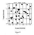
- Figure 21 is a graph illustrating the maximum variation of groove location relative to the mean location for three different sample stamped parts, each stamped part having 12 grooves.
- Figure 21 shows the excellent part-to-part repeatability.
- the maximum groove location relative to the mean location is ⁇ 160 nm along the x-axis and ⁇ 190 nm along the y-axis, demonstrating the submicron capability of the ultra precision stamping process.
- Figure 15 is a perspective view of a formed multi-fiber sleeve 1400.
- the sleeve 1400 can replace the pins typically used for alignment of two multi-fiber connectors.
- the outside dimensions of the multi-fiber ferrule must be designed to match the inside dimensions of the multi-fiber sleeve 1400. This must be done to sub-micron tolerances to assure proper fiber alignment and to minimize optical loss.
Landscapes
- Physics & Mathematics (AREA)
- General Physics & Mathematics (AREA)
- Optics & Photonics (AREA)
- Engineering & Computer Science (AREA)
- Mechanical Engineering (AREA)
- Life Sciences & Earth Sciences (AREA)
- Forests & Forestry (AREA)
- Mechanical Coupling Of Light Guides (AREA)
- Shaping Metal By Deep-Drawing, Or The Like (AREA)
- Optical Couplings Of Light Guides (AREA)
- Punching Or Piercing (AREA)
- Light Receiving Elements (AREA)
- Details Of Cutting Devices (AREA)
- Press Drives And Press Lines (AREA)
- Perforating, Stamping-Out Or Severing By Means Other Than Cutting (AREA)
Applications Claiming Priority (9)
| Application Number | Priority Date | Filing Date | Title |
|---|---|---|---|
| US620851 | 1990-11-30 | ||
| US40392402P | 2002-08-16 | 2002-08-16 | |
| US40392502P | 2002-08-16 | 2002-08-16 | |
| US40392602P | 2002-08-16 | 2002-08-16 | |
| US403924P | 2002-08-16 | ||
| US403925P | 2002-08-16 | ||
| US403926P | 2002-08-16 | ||
| US10/620,851 US7343770B2 (en) | 2002-08-16 | 2003-07-15 | Stamping system for manufacturing high tolerance parts |
| PCT/US2003/025939 WO2004017110A2 (en) | 2002-08-16 | 2003-08-18 | Stamping system for manufacturing high tolerance parts |
Related Child Applications (1)
| Application Number | Title | Priority Date | Filing Date |
|---|---|---|---|
| EP07020686 Division | 2007-10-23 |
Publications (2)
| Publication Number | Publication Date |
|---|---|
| EP1536931A2 EP1536931A2 (en) | 2005-06-08 |
| EP1536931B1 true EP1536931B1 (en) | 2008-03-19 |
Family
ID=31892260
Family Applications (3)
| Application Number | Title | Priority Date | Filing Date |
|---|---|---|---|
| EP20030788647 Expired - Lifetime EP1535097B1 (en) | 2002-08-16 | 2003-08-18 | High precision optoelectronic components |
| EP20030770241 Expired - Lifetime EP1536931B1 (en) | 2002-08-16 | 2003-08-18 | Stamping system for manufacturing high tolerance parts |
| EP20080010892 Withdrawn EP1961504A3 (en) | 2002-08-16 | 2003-08-18 | Process for producing high precision optoelectronic components |
Family Applications Before (1)
| Application Number | Title | Priority Date | Filing Date |
|---|---|---|---|
| EP20030788647 Expired - Lifetime EP1535097B1 (en) | 2002-08-16 | 2003-08-18 | High precision optoelectronic components |
Family Applications After (1)
| Application Number | Title | Priority Date | Filing Date |
|---|---|---|---|
| EP20080010892 Withdrawn EP1961504A3 (en) | 2002-08-16 | 2003-08-18 | Process for producing high precision optoelectronic components |
Country Status (14)
| Country | Link |
|---|---|
| US (1) | US7343770B2 (es) |
| EP (3) | EP1535097B1 (es) |
| JP (4) | JP4763287B2 (es) |
| KR (5) | KR101139562B1 (es) |
| CN (2) | CN100586673C (es) |
| AT (2) | ATE398786T1 (es) |
| AU (2) | AU2003278715B2 (es) |
| BR (2) | BR0313728B1 (es) |
| CA (2) | CA2495231C (es) |
| DE (2) | DE60319843T2 (es) |
| DK (2) | DK1536931T3 (es) |
| ES (2) | ES2306911T3 (es) |
| MX (2) | MXPA05001777A (es) |
| WO (2) | WO2004017117A2 (es) |
Families Citing this family (60)
| Publication number | Priority date | Publication date | Assignee | Title |
|---|---|---|---|---|
| US8276426B2 (en) * | 2007-03-21 | 2012-10-02 | Magnetic Metals Corporation | Laminated magnetic cores |
| FR2913898B1 (fr) * | 2007-03-23 | 2009-05-08 | Alcan Rhenalu Sa | Element structural en alliage d'aluminium incluant un capteur optique. |
| US8929702B2 (en) * | 2007-05-21 | 2015-01-06 | Schlumberger Technology Corporation | Modular opto-electrical cable unit |
| CN102033273B (zh) | 2009-09-24 | 2013-10-02 | 华为技术有限公司 | 一种光模块 |
| JP5371670B2 (ja) * | 2009-10-05 | 2013-12-18 | 株式会社フジクラ | 光ファイバ及びその製造方法 |
| CN101866036A (zh) * | 2010-06-17 | 2010-10-20 | 深圳日海通讯技术股份有限公司 | 光纤对中结构 |
| RU2638965C2 (ru) | 2011-04-05 | 2017-12-19 | Нанопресижен Продактс, Инк. | Соединительный зажим для оптических волокон с пазами для обжима открытых волокон |
| CN102243347B (zh) * | 2011-07-16 | 2013-01-23 | 无锡帝宝应用材料高科技有限公司 | 开放式感应光纤 |
| MX2014004575A (es) | 2011-10-17 | 2014-08-22 | Schlumberger Technology Bv | Cable de doble uso con envoltura de fibra optica para su uso en operaciones de perforacion de pozos. |
| EP2773992A1 (en) | 2011-11-02 | 2014-09-10 | Nanoprecision Products, Inc. | Castellated optical fiber cable retention structure |
| US8571364B2 (en) * | 2011-11-09 | 2013-10-29 | Alcon Research, Ltd. | Multi-spot laser probe with faceted optical element |
| US10302876B2 (en) * | 2012-02-16 | 2019-05-28 | Te Connectivity Corporation | Multi-channel optical insert |
| US20160274318A1 (en) | 2012-03-05 | 2016-09-22 | Nanoprecision Products, Inc. | Optical bench subassembly having integrated photonic device |
| US20130294732A1 (en) * | 2012-03-05 | 2013-11-07 | Nanoprecision Products, Inc. | Hermetic optical fiber alignment assembly having integrated optical element |
| CA2865800C (en) | 2012-03-05 | 2021-06-15 | Nanoprecision Products, Inc. | Coupling device having a structured reflective surface for coupling input/output of an optical fiber |
| US9782814B2 (en) | 2012-03-05 | 2017-10-10 | Nanoprecision Products, Inc. | Stamping to form a composite structure of dissimilar materials having structured features |
| WO2013151582A1 (en) | 2012-04-05 | 2013-10-10 | Nanoprecision Products, Inc. | High density multi-fiber for optical fiber connector |
| CA2869770A1 (en) * | 2012-04-11 | 2014-01-16 | Nanoprecision Products, Inc. | Optical fiber connector ferrule having curved external alignment surface |
| BR112014025229A2 (pt) * | 2012-04-11 | 2017-10-24 | Nanoprecision Products Inc | montagem de alinhamento de fibra óptica hermética |
| GB2518774B (en) | 2012-06-28 | 2020-01-29 | Schlumberger Holdings | High power opto-electrical cable with multiple power and telemetry paths |
| RU2537408C2 (ru) * | 2012-09-18 | 2015-01-10 | Федеральное государственное бюджетное образовательное учреждение высшего профессионального образования "Воронежский государственный технический университет" | Способ объемной штамповки на механическом прессе |
| KR101406036B1 (ko) * | 2012-11-01 | 2014-06-11 | 한국건설기술연구원 | 센서가 이식된 반원형 단면의 강선을 결합한 심선을 이용한 강연선의 제작방법 |
| WO2015017739A1 (en) | 2013-07-31 | 2015-02-05 | Nanoprecision Products, Inc. | Foldover optical fiber ferrule assembly |
| US9327369B2 (en) * | 2014-03-11 | 2016-05-03 | Asia Vital Components Co., Ltd. | Method of manufacturing thermal module with enhanced assembling structure |
| US9744582B2 (en) * | 2014-04-30 | 2017-08-29 | Fca Us Llc | Wear tolerance indicator for stamping dies |
| WO2015176038A1 (en) | 2014-05-15 | 2015-11-19 | Nanoprecision Products, Inc. | Stamping to form a composite structure of dissimilar materials having structured features |
| MX2016014892A (es) | 2014-05-15 | 2017-03-07 | Nanoprecision Products Inc | Conector optico desmontable para dispositivos optoelectronicos. |
| US9897769B2 (en) * | 2014-05-23 | 2018-02-20 | Nanoprecision Products, Inc. | Vision-based passive alignment of an optical fiber subassembly to an optoelectronic device |
| CA2967365A1 (en) | 2014-11-12 | 2016-05-19 | Nanoprecision Products, Inc. | A method of laser polishing a connectorized optical fiber and a connectorized optical fiber formed in accordance therewith |
| US9443040B2 (en) * | 2015-01-06 | 2016-09-13 | Ford Global Technologies, Llc | Method of forming hemming tool |
| US11725468B2 (en) | 2015-01-26 | 2023-08-15 | Schlumberger Technology Corporation | Electrically conductive fiber optic slickline for coiled tubing operations |
| USD773553S1 (en) * | 2015-02-18 | 2016-12-06 | Stewart-Macdonald Manufacturing Company | Stringed instrument work station |
| AU2016235324B2 (en) | 2015-03-22 | 2021-05-20 | Cudoquanta Florida, Inc. | Optical bench subassembly having integrated photonic device |
| EP3274751A1 (en) | 2015-03-22 | 2018-01-31 | Nanoprecision Products, Inc. | Axial preload for demountable connectors |
| CN105022122B (zh) * | 2015-04-29 | 2017-05-31 | 中航光电科技股份有限公司 | 保偏光纤连接器的接触件部件制作装置及制作方法 |
| WO2017027863A1 (en) | 2015-08-12 | 2017-02-16 | Nanoprecision Products, Inc. | Stamped solar collector concentrator system |
| WO2017027864A1 (en) | 2015-08-12 | 2017-02-16 | Nanoprecision Products, Inc. | Multiplexer/demultiplexer using stamped optical bench with micro mirrors |
| WO2017070713A1 (en) | 2015-10-23 | 2017-04-27 | Nanoprecision Products, Inc. | Hermetic optical subassembly |
| US9880366B2 (en) | 2015-10-23 | 2018-01-30 | Nanoprecision Products, Inc. | Hermetic optical subassembly |
| WO2017161061A1 (en) | 2016-03-15 | 2017-09-21 | Nanoprecision Products, Inc. | Optical alignment of an optical subassembly to an optoelectronic device |
| US10049789B2 (en) | 2016-06-09 | 2018-08-14 | Schlumberger Technology Corporation | Compression and stretch resistant components and cables for oilfield applications |
| CA3034099A1 (en) | 2016-08-17 | 2018-02-22 | Nanoprecision Products, Inc. | Optical fiber connector ferrule assembly having single reflective surface for beam expansion and expanded beam connector incorporating same |
| KR20190033632A (ko) * | 2016-08-17 | 2019-03-29 | 나노프리시젼 프로덕츠 인코포레이션 | 빔 확장을 위한 이중 반사 표면을 갖는 광섬유 연결부 페룰 조립체 및 이를 포함하는 확장형 빔 연결부 |
| US10739535B2 (en) | 2016-09-06 | 2020-08-11 | Cudoquanta Florida, Inc. | Process for reshaping and resizing grooves in optical fiber ferrules |
| US20180128991A1 (en) * | 2016-09-06 | 2018-05-10 | Nanoprecision Products, Inc. | High-precision fixture for aligning optical fiber ferrules for processing and processes using same |
| WO2018048966A1 (en) | 2016-09-06 | 2018-03-15 | Nanoprecision Products, Inc. | Fixture for reshaping and resizing grooves in optical fiber ferrules and process incorporating same |
| WO2018195094A1 (en) * | 2017-04-18 | 2018-10-25 | Commscope Technologies Llc | Fiber optic cable puncture press |
| JP2022509357A (ja) | 2018-10-23 | 2022-01-20 | クードクアンタ フロリダ インコーポレイテッド | アラインメントカプラを用いた光学コネクタおよび光学ベンチベースコネクタの取外し可能な接続 |
| CN109500242B (zh) * | 2018-11-16 | 2023-07-25 | 宁波横河精密工业股份有限公司 | 一种汽车天窗导轨多型面成型加工冲压模具及其冲压方法 |
| EP4100776A1 (en) | 2020-02-03 | 2022-12-14 | Senko Advanced Components Inc. | Elastic averaging coupling |
| WO2022005963A1 (en) * | 2020-06-30 | 2022-01-06 | Gates Corporation | Welded ferrule and method of making same |
| CN112078178B (zh) * | 2020-09-04 | 2022-08-26 | 太原理工大学 | 一种自动退模式压药模具 |
| CN113305193B (zh) * | 2021-06-10 | 2023-05-05 | 江西时代包装供应链管理有限公司 | 金属包装容器加工用冲压装备 |
| CN114749539A (zh) * | 2022-03-01 | 2022-07-15 | 江门市利华实业有限公司 | 一种床侧管加工生产线 |
| JP7502806B2 (ja) * | 2022-03-05 | 2024-06-19 | 檜山工業株式会社 | ファイバアレイ及びその製造方法 |
| WO2023201378A1 (en) | 2022-04-15 | 2023-10-19 | Senko Advanced Components, Inc. | A laser beam module package incorporating stamped metal freeform reflective optics |
| CN115193987B (zh) * | 2022-07-14 | 2023-05-30 | 江苏南方永磁科技有限公司 | 一种钕铁硼磁体成型压制装置 |
| WO2024059724A1 (en) | 2022-09-14 | 2024-03-21 | Senko Advanced Components, Inc. | Configurable optical connector module |
| CN115338282B (zh) * | 2022-10-17 | 2023-03-24 | 南通长石科技有限公司 | 镁合金锻件产品冲压成形系统及冲压成形方法 |
| WO2024092262A1 (en) | 2022-10-27 | 2024-05-02 | Senko Advanced Components, Inc. | Elastic averaging coupling |
Family Cites Families (76)
| Publication number | Priority date | Publication date | Assignee | Title |
|---|---|---|---|---|
| US2336982A (en) | 1940-05-14 | 1943-12-14 | Hardy Metallurg Company | Press |
| US3461762A (en) * | 1967-03-06 | 1969-08-19 | Unittool Punch & Die Co Inc | Punch and die unit |
| US3568855A (en) * | 1968-05-27 | 1971-03-09 | Halliburton Co | Hydraulic cushioning apparatus for railway cars |
| US3568555A (en) * | 1968-09-11 | 1971-03-09 | Porter Precision Products Co | Guidepost construction for die sets |
| US3709083A (en) | 1971-03-18 | 1973-01-09 | N Doherty | Electrically actuated punch press |
| US3768295A (en) * | 1972-02-08 | 1973-10-30 | Reynolds Metals Co | Forming apparatus and method |
| JPS529428B2 (es) | 1973-02-06 | 1977-03-16 | ||
| US3972585A (en) | 1975-02-13 | 1976-08-03 | Northern Electric Company Limited | Connectors for optical fibers |
| US3933071A (en) * | 1975-03-27 | 1976-01-20 | Onondaga Tool Corporation | Shearproof punch |
| US4030336A (en) | 1976-07-09 | 1977-06-21 | Anatoly Sergeevich Grigorenko | Hydraulic protection device for presses |
| US4103718A (en) * | 1977-10-06 | 1978-08-01 | Honeywell Information Systems Inc. | Apparatus for cutting and forming flexible beam leads of an integrated circuit chip |
| US4292862A (en) | 1979-09-12 | 1981-10-06 | Owens-Corning Fiberglas Corporation | Method and apparatus for production of a stream feeder |
| JPS5643616A (en) * | 1979-09-19 | 1981-04-22 | Nippon Telegr & Teleph Corp <Ntt> | Assembling method of base part of multicore connector of optical fiber |
| US4458985A (en) | 1981-10-16 | 1984-07-10 | International Business Machines Corporation | Optical fiber connector |
| JPS58100112A (ja) * | 1981-12-11 | 1983-06-14 | Fujitsu Ltd | 光マルチコネクタアダプタ |
| DE3380453D1 (en) * | 1982-06-05 | 1989-09-28 | Amp Inc | Optical fibre termination method, terminal, splice, and connector therefor |
| EP0201944B1 (en) | 1982-06-05 | 1990-03-07 | Amp Incorporated | Connector for terminating an optical fibre |
| JPS6035045Y2 (ja) * | 1983-03-23 | 1985-10-18 | 株式会社日立製作所 | 光フアイバ−接続器 |
| US4524582A (en) | 1983-03-31 | 1985-06-25 | Cincinnati Incorporated | Control system for hydraulic presses |
| US4555968A (en) | 1984-06-07 | 1985-12-03 | Preco Industries, Inc. | Web fed die cutting press having automatic 3-axis die registration system |
| JPS61153604A (ja) * | 1984-12-27 | 1986-07-12 | Fujitsu Ltd | 光コネクタフエル−ル構造 |
| JPS61275707A (ja) * | 1985-05-30 | 1986-12-05 | Nec Corp | 光フアイバコネクタ構造 |
| JPS62121413A (ja) * | 1985-11-22 | 1987-06-02 | Nec Corp | 光コネクタ |
| JPS635311A (ja) * | 1986-06-25 | 1988-01-11 | Oputosu:Kk | 光フアイバ用中継アダプタ |
| JPH037118Y2 (es) * | 1987-02-27 | 1991-02-21 | ||
| JPH08398B2 (ja) | 1987-04-24 | 1996-01-10 | 潮工業有限会社 | 薄板状物の穿孔装置及び穿孔装置用パンチングユニツト |
| DE3761517D1 (de) | 1987-07-14 | 1990-03-01 | Inovan Stroebe | Lichtwellenleiter-verbinder. |
| JPS6479709A (en) * | 1987-09-21 | 1989-03-24 | Sumitomo Electric Industries | Optical connector coupling sleeve |
| US4926677A (en) | 1987-12-03 | 1990-05-22 | Kurt Waldner | Die apparatus |
| JPH01262506A (ja) * | 1988-04-14 | 1989-10-19 | Hirose Electric Co Ltd | 多心光ファイバケーブルの永久接続装置およびその接続方法 |
| JPH039920Y2 (es) * | 1988-06-29 | 1991-03-12 | ||
| US4887452A (en) * | 1988-12-15 | 1989-12-19 | Amp Incorporated | Sprocket-type strip feed |
| JPH0681678B2 (ja) * | 1989-05-11 | 1994-10-19 | 株式会社伊原工業 | プレス装置 |
| IT1240310B (it) * | 1989-07-24 | 1993-12-07 | Pirelli Cavi Spa | Gruppo di connessione separabile per fibre ottiche riunite a nastro e relativo metodo di realizzazione. |
| IT1237091B (it) | 1989-10-17 | 1993-05-18 | Pirelli Cavi Spa | Gruppo compatto di connessione separabile per fibre ottiche riunite a nastro. |
| US5113736A (en) | 1990-06-26 | 1992-05-19 | Meyerle George M | Electromagnetically driven punch press with magnetically isolated removable electromagnetic thrust motor |
| DE4041030A1 (de) | 1990-12-20 | 1992-07-02 | Siemens Ag | Krimpspleiss |
| JPH04288997A (ja) * | 1991-03-19 | 1992-10-14 | Kobe Steel Ltd | 鍛造プレスのクッション装置 |
| AU635172B2 (en) * | 1991-05-13 | 1993-03-11 | Nippon Telegraph & Telephone Corporation | Multifiber optical connector plug with low reflection and low insertion loss |
| JPH0545536A (ja) * | 1991-08-13 | 1993-02-23 | Fujitsu Ltd | 多心光コネクタ |
| US5155787A (en) * | 1991-09-06 | 1992-10-13 | Minnesota Mining And Manufacturing Company | Multiple optical fiber splice element having ramped porch |
| JPH06118266A (ja) * | 1992-10-06 | 1994-04-28 | Nippon Telegr & Teleph Corp <Ntt> | 光端末部品 |
| US5319728A (en) | 1993-05-20 | 1994-06-07 | Adc Telecommunication, Inc. | High return loss fixed attenuator |
| EP0641644A1 (de) | 1993-09-02 | 1995-03-08 | Maschinenfabrik Müller-Weingarten AG | Verfahren zur Regelung des Antriebs einer hydraulischen Presse und Vorrichtung zur Durchführung des Verfahrens |
| JPH07248434A (ja) * | 1994-03-08 | 1995-09-26 | Hitachi Cable Ltd | 光ファイバアレイおよび光ファイバアレイ用アダプタ |
| JPH07308799A (ja) * | 1994-05-17 | 1995-11-28 | Kurimoto Ltd | 金属裁断屑の圧縮成形プレス |
| JP2824401B2 (ja) | 1994-12-05 | 1998-11-11 | 旭コーデン株式会社 | 光ファイバー保持装置及び同装置に用いる管状体の製造法 |
| JP3725215B2 (ja) * | 1995-09-29 | 2005-12-07 | 株式会社フジクラ | 光ファイバ接続器 |
| JP3289584B2 (ja) * | 1995-11-30 | 2002-06-10 | 株式会社デンソー | 板材のプレス加工方法およびプレス加工装置 |
| US6045270A (en) | 1995-12-22 | 2000-04-04 | Methode Electronics, Inc. | Massive parallel optical interconnect system |
| JPH09267125A (ja) * | 1996-03-30 | 1997-10-14 | Tsugiyoshi Osawa | 微細孔パイプの製造方法 |
| JP3630845B2 (ja) * | 1996-05-07 | 2005-03-23 | 株式会社フジクラ | 光ファイバ接続器 |
| WO1998015381A1 (en) | 1996-10-10 | 1998-04-16 | Tyco Submarine Systems Ltd. | Press apparatus for fiber-optic plug |
| JP3515305B2 (ja) | 1997-01-16 | 2004-04-05 | 株式会社フジクラ | 光コネクタ |
| JPH10282367A (ja) * | 1997-04-02 | 1998-10-23 | Toyo Commun Equip Co Ltd | 光コネクタ |
| US6315971B1 (en) * | 1997-04-09 | 2001-11-13 | Cabot Corporation | Process for producing low density gel compositions |
| JPH11174274A (ja) * | 1997-12-12 | 1999-07-02 | Sumitomo Electric Ind Ltd | 光ファイバアレイおよび金型の製造方法 |
| JPH11194226A (ja) * | 1997-12-26 | 1999-07-21 | Hoya Corp | 光ファイバ固定用部材、光ファイバアレイおよび光導波路モジュール |
| US6122952A (en) | 1998-04-09 | 2000-09-26 | Hutchinson Technology Incorporated | Multiple actuation press for metal working and method of metal forming |
| JP3461724B2 (ja) * | 1998-06-11 | 2003-10-27 | 株式会社フジクラ | ファイバグレーティング付きの光コネクタフェルール |
| JP2000033494A (ja) * | 1998-07-16 | 2000-02-02 | Aida Eng Ltd | 下死点停留機構内蔵プレス |
| US6314852B1 (en) | 1998-08-03 | 2001-11-13 | International Business Machines Corporation | Gang punch tool assembly |
| JP4521073B2 (ja) * | 1999-04-06 | 2010-08-11 | 株式会社アマダ | 追抜き金型 |
| US6311597B1 (en) * | 1999-05-24 | 2001-11-06 | Humdinger, Inc. | Self-guiding punch and die set |
| JP2000343144A (ja) | 1999-06-04 | 2000-12-12 | Denso Corp | プレス成形品の製造方法 |
| JP3378216B2 (ja) * | 1999-08-25 | 2003-02-17 | 株式会社貴匠技研 | 光ファイバ接続用スリーブ及びその製造方法 |
| JP2001091783A (ja) * | 1999-09-20 | 2001-04-06 | Kyocera Corp | 光通信用割スリーブ及びその製造方法 |
| WO2001061396A1 (fr) * | 2000-02-16 | 2001-08-23 | Monobe Engineering Co., Ltd. | Procede de fabrication de passe-fil |
| US6416334B1 (en) | 2000-03-24 | 2002-07-09 | Paul J. Plishner | Combination multi-conductor/optical fiber connector |
| US20010051026A1 (en) | 2000-04-06 | 2001-12-13 | Steinberg Dan A. | Optical fiber ferrule made from dry etched parts |
| JP2002160017A (ja) * | 2000-11-27 | 2002-06-04 | Teijin Seiki Precision Kk | 帯状板材の加工方法及び加工機 |
| JP2002160098A (ja) * | 2000-11-27 | 2002-06-04 | Matsushita Electric Works Ltd | プレス成形装置 |
| US20020114591A1 (en) | 2001-02-22 | 2002-08-22 | International Business Machines Corporation | Optical subassembly for fiber arrays with a 90 degree conductor turn |
| GB2385550A (en) * | 2002-02-20 | 2003-08-27 | Colin Maxwell Wade | Punch for a ductile material joining tool |
| JP2005037450A (ja) * | 2003-07-15 | 2005-02-10 | Yazaki Corp | フェルールと連鎖状フェルール |
| JP4279126B2 (ja) * | 2003-12-11 | 2009-06-17 | 古河電気工業株式会社 | 光ファイバの固定構造及び光コネクタ |
-
2003
- 2003-07-15 US US10/620,851 patent/US7343770B2/en active Active
- 2003-08-18 JP JP2004529130A patent/JP4763287B2/ja not_active Expired - Fee Related
- 2003-08-18 MX MXPA05001777A patent/MXPA05001777A/es active IP Right Grant
- 2003-08-18 JP JP2004529131A patent/JP2006500604A/ja not_active Withdrawn
- 2003-08-18 CA CA002495231A patent/CA2495231C/en not_active Expired - Lifetime
- 2003-08-18 EP EP20030788647 patent/EP1535097B1/en not_active Expired - Lifetime
- 2003-08-18 CN CN03824052A patent/CN100586673C/zh not_active Expired - Fee Related
- 2003-08-18 MX MXPA05001778A patent/MXPA05001778A/es active IP Right Grant
- 2003-08-18 CA CA 2495268 patent/CA2495268C/en not_active Expired - Fee Related
- 2003-08-18 DK DK03770241T patent/DK1536931T3/da active
- 2003-08-18 DK DK03788647T patent/DK1535097T3/da active
- 2003-08-18 KR KR1020057002633A patent/KR101139562B1/ko active IP Right Grant
- 2003-08-18 KR KR1020127007725A patent/KR101278321B1/ko active IP Right Grant
- 2003-08-18 CN CNB038241595A patent/CN100504474C/zh not_active Expired - Fee Related
- 2003-08-18 WO PCT/US2003/025940 patent/WO2004017117A2/en active Application Filing
- 2003-08-18 ES ES03788647T patent/ES2306911T3/es not_active Expired - Lifetime
- 2003-08-18 EP EP20030770241 patent/EP1536931B1/en not_active Expired - Lifetime
- 2003-08-18 EP EP20080010892 patent/EP1961504A3/en not_active Withdrawn
- 2003-08-18 KR KR1020127005613A patent/KR20120037513A/ko not_active Application Discontinuation
- 2003-08-18 AU AU2003278715A patent/AU2003278715B2/en not_active Ceased
- 2003-08-18 KR KR1020107016759A patent/KR20100102683A/ko not_active Application Discontinuation
- 2003-08-18 AT AT03788647T patent/ATE398786T1/de not_active IP Right Cessation
- 2003-08-18 DE DE2003619843 patent/DE60319843T2/de not_active Expired - Lifetime
- 2003-08-18 DE DE60321686T patent/DE60321686D1/de not_active Expired - Lifetime
- 2003-08-18 BR BRPI0313728-7B1A patent/BR0313728B1/pt not_active IP Right Cessation
- 2003-08-18 KR KR1020057002627A patent/KR101059611B1/ko active IP Right Grant
- 2003-08-18 BR BR0313533A patent/BR0313533A/pt not_active Application Discontinuation
- 2003-08-18 ES ES03770241T patent/ES2303602T3/es not_active Expired - Lifetime
- 2003-08-18 WO PCT/US2003/025939 patent/WO2004017110A2/en active Application Filing
- 2003-08-18 AU AU2003263930A patent/AU2003263930B2/en not_active Ceased
- 2003-08-18 AT AT03770241T patent/ATE389516T1/de not_active IP Right Cessation
-
2010
- 2010-07-02 JP JP2010152330A patent/JP5426490B2/ja not_active Expired - Lifetime
-
2013
- 2013-08-16 JP JP2013169228A patent/JP6110255B2/ja not_active Expired - Fee Related
Also Published As
Similar Documents
| Publication | Publication Date | Title |
|---|---|---|
| EP1536931B1 (en) | Stamping system for manufacturing high tolerance parts | |
| AU766753B2 (en) | Self-guiding punch and die set | |
| US7311449B2 (en) | High precision optoelectronic components | |
| IE881843L (en) | Tool guidance system for forming machine | |
| RU2380186C2 (ru) | Установка для изготовления деталей, система для изготовления деталей, способ изготовления деталей и деталь, полученная упомянутым способом | |
| US4866976A (en) | Apparatus for the metal working of components | |
| JP2024026297A (ja) | 工具ユニット、工具ユニットを保持するプレス機、工具ユニットをプレス機のホルダ内に作動可能に配置する方法 | |
| JPS642455B2 (es) | ||
| JP2006021213A (ja) | 鍛造金型装置 |
Legal Events
| Date | Code | Title | Description |
|---|---|---|---|
| PUAI | Public reference made under article 153(3) epc to a published international application that has entered the european phase |
Free format text: ORIGINAL CODE: 0009012 |
|
| 17P | Request for examination filed |
Effective date: 20050314 |
|
| AK | Designated contracting states |
Kind code of ref document: A2 Designated state(s): AT BE BG CH CY CZ DE DK EE ES FI FR GB GR HU IE IT LI LU MC NL PT RO SE SI SK TR |
|
| AX | Request for extension of the european patent |
Extension state: AL LT LV MK |
|
| DAX | Request for extension of the european patent (deleted) | ||
| 17Q | First examination report despatched |
Effective date: 20051013 |
|
| RIN1 | Information on inventor provided before grant (corrected) |
Inventor name: HARRIS, DAN Inventor name: BARNOSKI, MICHAEL, K. Inventor name: PRINZ, FRITZ Inventor name: TARASYUK, ALEX Inventor name: COHEN, DAVID Inventor name: KANG, SANGKYUN Inventor name: LEVI, ANTHONY Inventor name: PINILLA, MIGUEL |
|
| GRAP | Despatch of communication of intention to grant a patent |
Free format text: ORIGINAL CODE: EPIDOSNIGR1 |
|
| GRAS | Grant fee paid |
Free format text: ORIGINAL CODE: EPIDOSNIGR3 |
|
| GRAA | (expected) grant |
Free format text: ORIGINAL CODE: 0009210 |
|
| AK | Designated contracting states |
Kind code of ref document: B1 Designated state(s): AT BE BG CH CY CZ DE DK EE ES FI FR GB GR HU IE IT LI LU MC NL PT RO SE SI SK TR |
|
| REG | Reference to a national code |
Ref country code: GB Ref legal event code: FG4D |
|
| REG | Reference to a national code |
Ref country code: CH Ref legal event code: EP |
|
| REF | Corresponds to: |
Ref document number: 60319843 Country of ref document: DE Date of ref document: 20080430 Kind code of ref document: P |
|
| REG | Reference to a national code |
Ref country code: IE Ref legal event code: FG4D |
|
| REG | Reference to a national code |
Ref country code: DK Ref legal event code: T3 |
|
| REG | Reference to a national code |
Ref country code: ES Ref legal event code: FG2A Ref document number: 2303602 Country of ref document: ES Kind code of ref document: T3 |
|
| PG25 | Lapsed in a contracting state [announced via postgrant information from national office to epo] |
Ref country code: AT Free format text: LAPSE BECAUSE OF FAILURE TO SUBMIT A TRANSLATION OF THE DESCRIPTION OR TO PAY THE FEE WITHIN THE PRESCRIBED TIME-LIMIT Effective date: 20080319 |
|
| PG25 | Lapsed in a contracting state [announced via postgrant information from national office to epo] |
Ref country code: SI Free format text: LAPSE BECAUSE OF FAILURE TO SUBMIT A TRANSLATION OF THE DESCRIPTION OR TO PAY THE FEE WITHIN THE PRESCRIBED TIME-LIMIT Effective date: 20080319 |
|
| PG25 | Lapsed in a contracting state [announced via postgrant information from national office to epo] |
Ref country code: CZ Free format text: LAPSE BECAUSE OF FAILURE TO SUBMIT A TRANSLATION OF THE DESCRIPTION OR TO PAY THE FEE WITHIN THE PRESCRIBED TIME-LIMIT Effective date: 20080319 Ref country code: PT Free format text: LAPSE BECAUSE OF FAILURE TO SUBMIT A TRANSLATION OF THE DESCRIPTION OR TO PAY THE FEE WITHIN THE PRESCRIBED TIME-LIMIT Effective date: 20080826 Ref country code: SK Free format text: LAPSE BECAUSE OF FAILURE TO SUBMIT A TRANSLATION OF THE DESCRIPTION OR TO PAY THE FEE WITHIN THE PRESCRIBED TIME-LIMIT Effective date: 20080319 |
|
| PG25 | Lapsed in a contracting state [announced via postgrant information from national office to epo] |
Ref country code: RO Free format text: LAPSE BECAUSE OF FAILURE TO SUBMIT A TRANSLATION OF THE DESCRIPTION OR TO PAY THE FEE WITHIN THE PRESCRIBED TIME-LIMIT Effective date: 20080319 |
|
| ET | Fr: translation filed | ||
| PLBE | No opposition filed within time limit |
Free format text: ORIGINAL CODE: 0009261 |
|
| STAA | Information on the status of an ep patent application or granted ep patent |
Free format text: STATUS: NO OPPOSITION FILED WITHIN TIME LIMIT |
|
| 26N | No opposition filed |
Effective date: 20081222 |
|
| REG | Reference to a national code |
Ref country code: DK Ref legal event code: EBP |
|
| PG25 | Lapsed in a contracting state [announced via postgrant information from national office to epo] |
Ref country code: MC Free format text: LAPSE BECAUSE OF NON-PAYMENT OF DUE FEES Effective date: 20080831 |
|
| PG25 | Lapsed in a contracting state [announced via postgrant information from national office to epo] |
Ref country code: BG Free format text: LAPSE BECAUSE OF FAILURE TO SUBMIT A TRANSLATION OF THE DESCRIPTION OR TO PAY THE FEE WITHIN THE PRESCRIBED TIME-LIMIT Effective date: 20080619 Ref country code: EE Free format text: LAPSE BECAUSE OF FAILURE TO SUBMIT A TRANSLATION OF THE DESCRIPTION OR TO PAY THE FEE WITHIN THE PRESCRIBED TIME-LIMIT Effective date: 20080319 |
|
| PG25 | Lapsed in a contracting state [announced via postgrant information from national office to epo] |
Ref country code: DK Free format text: LAPSE BECAUSE OF NON-PAYMENT OF DUE FEES Effective date: 20080831 |
|
| PG25 | Lapsed in a contracting state [announced via postgrant information from national office to epo] |
Ref country code: CY Free format text: LAPSE BECAUSE OF FAILURE TO SUBMIT A TRANSLATION OF THE DESCRIPTION OR TO PAY THE FEE WITHIN THE PRESCRIBED TIME-LIMIT Effective date: 20080319 |
|
| REG | Reference to a national code |
Ref country code: CH Ref legal event code: NV Representative=s name: MURGITROYD & COMPANY |
|
| PG25 | Lapsed in a contracting state [announced via postgrant information from national office to epo] |
Ref country code: HU Free format text: LAPSE BECAUSE OF FAILURE TO SUBMIT A TRANSLATION OF THE DESCRIPTION OR TO PAY THE FEE WITHIN THE PRESCRIBED TIME-LIMIT Effective date: 20080920 Ref country code: LU Free format text: LAPSE BECAUSE OF NON-PAYMENT OF DUE FEES Effective date: 20080818 |
|
| PG25 | Lapsed in a contracting state [announced via postgrant information from national office to epo] |
Ref country code: TR Free format text: LAPSE BECAUSE OF FAILURE TO SUBMIT A TRANSLATION OF THE DESCRIPTION OR TO PAY THE FEE WITHIN THE PRESCRIBED TIME-LIMIT Effective date: 20080319 |
|
| PG25 | Lapsed in a contracting state [announced via postgrant information from national office to epo] |
Ref country code: GR Free format text: LAPSE BECAUSE OF FAILURE TO SUBMIT A TRANSLATION OF THE DESCRIPTION OR TO PAY THE FEE WITHIN THE PRESCRIBED TIME-LIMIT Effective date: 20080620 |
|
| PG25 | Lapsed in a contracting state [announced via postgrant information from national office to epo] |
Ref country code: IT Free format text: LAPSE BECAUSE OF NON-PAYMENT OF DUE FEES Effective date: 20100818 |
|
| PGRI | Patent reinstated in contracting state [announced from national office to epo] |
Ref country code: IT Effective date: 20110616 |
|
| REG | Reference to a national code |
Ref country code: FR Ref legal event code: PLFP Year of fee payment: 14 |
|
| REG | Reference to a national code |
Ref country code: FR Ref legal event code: PLFP Year of fee payment: 15 |
|
| PGFP | Annual fee paid to national office [announced via postgrant information from national office to epo] |
Ref country code: NL Payment date: 20170829 Year of fee payment: 15 |
|
| PGFP | Annual fee paid to national office [announced via postgrant information from national office to epo] |
Ref country code: DE Payment date: 20170825 Year of fee payment: 15 Ref country code: ES Payment date: 20170915 Year of fee payment: 15 Ref country code: GB Payment date: 20170819 Year of fee payment: 15 Ref country code: FR Payment date: 20170816 Year of fee payment: 15 Ref country code: CH Payment date: 20170816 Year of fee payment: 15 Ref country code: FI Payment date: 20170825 Year of fee payment: 15 Ref country code: IT Payment date: 20170817 Year of fee payment: 15 |
|
| PGFP | Annual fee paid to national office [announced via postgrant information from national office to epo] |
Ref country code: BE Payment date: 20170828 Year of fee payment: 15 Ref country code: IE Payment date: 20170825 Year of fee payment: 15 Ref country code: DK Payment date: 20170828 Year of fee payment: 15 Ref country code: SE Payment date: 20170816 Year of fee payment: 15 |
|
| REG | Reference to a national code |
Ref country code: DE Ref legal event code: R119 Ref document number: 60319843 Country of ref document: DE |
|
| REG | Reference to a national code |
Ref country code: DK Ref legal event code: EBP Effective date: 20080831 Ref country code: DK Ref legal event code: EBP Effective date: 20180831 |
|
| REG | Reference to a national code |
Ref country code: CH Ref legal event code: PL |
|
| REG | Reference to a national code |
Ref country code: SE Ref legal event code: EUG |
|
| REG | Reference to a national code |
Ref country code: NL Ref legal event code: MM Effective date: 20180901 |
|
| GBPC | Gb: european patent ceased through non-payment of renewal fee |
Effective date: 20180818 |
|
| PG25 | Lapsed in a contracting state [announced via postgrant information from national office to epo] |
Ref country code: CH Free format text: LAPSE BECAUSE OF NON-PAYMENT OF DUE FEES Effective date: 20180831 Ref country code: LI Free format text: LAPSE BECAUSE OF NON-PAYMENT OF DUE FEES Effective date: 20180831 Ref country code: FI Free format text: LAPSE BECAUSE OF NON-PAYMENT OF DUE FEES Effective date: 20180818 |
|
| REG | Reference to a national code |
Ref country code: BE Ref legal event code: MM Effective date: 20180831 |
|
| REG | Reference to a national code |
Ref country code: IE Ref legal event code: MM4A |
|
| PG25 | Lapsed in a contracting state [announced via postgrant information from national office to epo] |
Ref country code: SE Free format text: LAPSE BECAUSE OF NON-PAYMENT OF DUE FEES Effective date: 20180819 |
|
| PG25 | Lapsed in a contracting state [announced via postgrant information from national office to epo] |
Ref country code: NL Free format text: LAPSE BECAUSE OF NON-PAYMENT OF DUE FEES Effective date: 20180901 |
|
| PG25 | Lapsed in a contracting state [announced via postgrant information from national office to epo] |
Ref country code: IE Free format text: LAPSE BECAUSE OF NON-PAYMENT OF DUE FEES Effective date: 20180818 Ref country code: IT Free format text: LAPSE BECAUSE OF NON-PAYMENT OF DUE FEES Effective date: 20180818 Ref country code: DK Free format text: LAPSE BECAUSE OF NON-PAYMENT OF DUE FEES Effective date: 20180831 Ref country code: DE Free format text: LAPSE BECAUSE OF NON-PAYMENT OF DUE FEES Effective date: 20190301 |
|
| PG25 | Lapsed in a contracting state [announced via postgrant information from national office to epo] |
Ref country code: BE Free format text: LAPSE BECAUSE OF NON-PAYMENT OF DUE FEES Effective date: 20180831 Ref country code: FR Free format text: LAPSE BECAUSE OF NON-PAYMENT OF DUE FEES Effective date: 20180831 |
|
| REG | Reference to a national code |
Ref country code: ES Ref legal event code: FD2A Effective date: 20190918 |
|
| PG25 | Lapsed in a contracting state [announced via postgrant information from national office to epo] |
Ref country code: GB Free format text: LAPSE BECAUSE OF NON-PAYMENT OF DUE FEES Effective date: 20180818 Ref country code: ES Free format text: LAPSE BECAUSE OF NON-PAYMENT OF DUE FEES Effective date: 20180819 |