EP1536405B1 - Dispositif d'affichage électroluminescent, panneau d'affichage, et sa méthode de commande - Google Patents
Dispositif d'affichage électroluminescent, panneau d'affichage, et sa méthode de commande Download PDFInfo
- Publication number
- EP1536405B1 EP1536405B1 EP04090384.1A EP04090384A EP1536405B1 EP 1536405 B1 EP1536405 B1 EP 1536405B1 EP 04090384 A EP04090384 A EP 04090384A EP 1536405 B1 EP1536405 B1 EP 1536405B1
- Authority
- EP
- European Patent Office
- Prior art keywords
- voltage
- electrode
- transistor
- data
- capacitor
- Prior art date
- Legal status (The legal status is an assumption and is not a legal conclusion. Google has not performed a legal analysis and makes no representation as to the accuracy of the status listed.)
- Active
Links
- 238000000034 method Methods 0.000 title claims description 18
- 239000003990 capacitor Substances 0.000 claims description 72
- 108091006146 Channels Proteins 0.000 claims description 5
- 108010075750 P-Type Calcium Channels Proteins 0.000 claims description 5
- 101150037603 cst-1 gene Proteins 0.000 claims 5
- 238000010586 diagram Methods 0.000 description 6
- 239000011159 matrix material Substances 0.000 description 5
- 239000010409 thin film Substances 0.000 description 4
- 108090000699 N-Type Calcium Channels Proteins 0.000 description 3
- 102000004129 N-Type Calcium Channels Human genes 0.000 description 3
- 239000011521 glass Substances 0.000 description 3
- 239000000758 substrate Substances 0.000 description 3
- 239000010408 film Substances 0.000 description 2
- 230000000593 degrading effect Effects 0.000 description 1
- 230000000694 effects Effects 0.000 description 1
- 230000005525 hole transport Effects 0.000 description 1
- AMGQUBHHOARCQH-UHFFFAOYSA-N indium;oxotin Chemical compound [In].[Sn]=O AMGQUBHHOARCQH-UHFFFAOYSA-N 0.000 description 1
- 239000002184 metal Substances 0.000 description 1
- 229910052751 metal Inorganic materials 0.000 description 1
- 238000012986 modification Methods 0.000 description 1
- 230000004048 modification Effects 0.000 description 1
- 230000003071 parasitic effect Effects 0.000 description 1
- -1 phosphorous organic compound Chemical class 0.000 description 1
Images


Classifications
-
- G—PHYSICS
- G09—EDUCATION; CRYPTOGRAPHY; DISPLAY; ADVERTISING; SEALS
- G09G—ARRANGEMENTS OR CIRCUITS FOR CONTROL OF INDICATING DEVICES USING STATIC MEANS TO PRESENT VARIABLE INFORMATION
- G09G3/00—Control arrangements or circuits, of interest only in connection with visual indicators other than cathode-ray tubes
- G09G3/20—Control arrangements or circuits, of interest only in connection with visual indicators other than cathode-ray tubes for presentation of an assembly of a number of characters, e.g. a page, by composing the assembly by combination of individual elements arranged in a matrix no fixed position being assigned to or needed to be assigned to the individual characters or partial characters
- G09G3/22—Control arrangements or circuits, of interest only in connection with visual indicators other than cathode-ray tubes for presentation of an assembly of a number of characters, e.g. a page, by composing the assembly by combination of individual elements arranged in a matrix no fixed position being assigned to or needed to be assigned to the individual characters or partial characters using controlled light sources
- G09G3/30—Control arrangements or circuits, of interest only in connection with visual indicators other than cathode-ray tubes for presentation of an assembly of a number of characters, e.g. a page, by composing the assembly by combination of individual elements arranged in a matrix no fixed position being assigned to or needed to be assigned to the individual characters or partial characters using controlled light sources using electroluminescent panels
- G09G3/32—Control arrangements or circuits, of interest only in connection with visual indicators other than cathode-ray tubes for presentation of an assembly of a number of characters, e.g. a page, by composing the assembly by combination of individual elements arranged in a matrix no fixed position being assigned to or needed to be assigned to the individual characters or partial characters using controlled light sources using electroluminescent panels semiconductive, e.g. using light-emitting diodes [LED]
- G09G3/3208—Control arrangements or circuits, of interest only in connection with visual indicators other than cathode-ray tubes for presentation of an assembly of a number of characters, e.g. a page, by composing the assembly by combination of individual elements arranged in a matrix no fixed position being assigned to or needed to be assigned to the individual characters or partial characters using controlled light sources using electroluminescent panels semiconductive, e.g. using light-emitting diodes [LED] organic, e.g. using organic light-emitting diodes [OLED]
- G09G3/3225—Control arrangements or circuits, of interest only in connection with visual indicators other than cathode-ray tubes for presentation of an assembly of a number of characters, e.g. a page, by composing the assembly by combination of individual elements arranged in a matrix no fixed position being assigned to or needed to be assigned to the individual characters or partial characters using controlled light sources using electroluminescent panels semiconductive, e.g. using light-emitting diodes [LED] organic, e.g. using organic light-emitting diodes [OLED] using an active matrix
- G09G3/3233—Control arrangements or circuits, of interest only in connection with visual indicators other than cathode-ray tubes for presentation of an assembly of a number of characters, e.g. a page, by composing the assembly by combination of individual elements arranged in a matrix no fixed position being assigned to or needed to be assigned to the individual characters or partial characters using controlled light sources using electroluminescent panels semiconductive, e.g. using light-emitting diodes [LED] organic, e.g. using organic light-emitting diodes [OLED] using an active matrix with pixel circuitry controlling the current through the light-emitting element
-
- G—PHYSICS
- G09—EDUCATION; CRYPTOGRAPHY; DISPLAY; ADVERTISING; SEALS
- G09G—ARRANGEMENTS OR CIRCUITS FOR CONTROL OF INDICATING DEVICES USING STATIC MEANS TO PRESENT VARIABLE INFORMATION
- G09G2300/00—Aspects of the constitution of display devices
- G09G2300/04—Structural and physical details of display devices
- G09G2300/0421—Structural details of the set of electrodes
- G09G2300/043—Compensation electrodes or other additional electrodes in matrix displays related to distortions or compensation signals, e.g. for modifying TFT threshold voltage in column driver
-
- G—PHYSICS
- G09—EDUCATION; CRYPTOGRAPHY; DISPLAY; ADVERTISING; SEALS
- G09G—ARRANGEMENTS OR CIRCUITS FOR CONTROL OF INDICATING DEVICES USING STATIC MEANS TO PRESENT VARIABLE INFORMATION
- G09G2300/00—Aspects of the constitution of display devices
- G09G2300/08—Active matrix structure, i.e. with use of active elements, inclusive of non-linear two terminal elements, in the pixels together with light emitting or modulating elements
- G09G2300/0809—Several active elements per pixel in active matrix panels
- G09G2300/0819—Several active elements per pixel in active matrix panels used for counteracting undesired variations, e.g. feedback or autozeroing
-
- G—PHYSICS
- G09—EDUCATION; CRYPTOGRAPHY; DISPLAY; ADVERTISING; SEALS
- G09G—ARRANGEMENTS OR CIRCUITS FOR CONTROL OF INDICATING DEVICES USING STATIC MEANS TO PRESENT VARIABLE INFORMATION
- G09G2300/00—Aspects of the constitution of display devices
- G09G2300/08—Active matrix structure, i.e. with use of active elements, inclusive of non-linear two terminal elements, in the pixels together with light emitting or modulating elements
- G09G2300/0809—Several active elements per pixel in active matrix panels
- G09G2300/0842—Several active elements per pixel in active matrix panels forming a memory circuit, e.g. a dynamic memory with one capacitor
-
- G—PHYSICS
- G09—EDUCATION; CRYPTOGRAPHY; DISPLAY; ADVERTISING; SEALS
- G09G—ARRANGEMENTS OR CIRCUITS FOR CONTROL OF INDICATING DEVICES USING STATIC MEANS TO PRESENT VARIABLE INFORMATION
- G09G2310/00—Command of the display device
- G09G2310/02—Addressing, scanning or driving the display screen or processing steps related thereto
- G09G2310/0243—Details of the generation of driving signals
- G09G2310/0251—Precharge or discharge of pixel before applying new pixel voltage
-
- G—PHYSICS
- G09—EDUCATION; CRYPTOGRAPHY; DISPLAY; ADVERTISING; SEALS
- G09G—ARRANGEMENTS OR CIRCUITS FOR CONTROL OF INDICATING DEVICES USING STATIC MEANS TO PRESENT VARIABLE INFORMATION
- G09G2310/00—Command of the display device
- G09G2310/02—Addressing, scanning or driving the display screen or processing steps related thereto
- G09G2310/0262—The addressing of the pixel, in a display other than an active matrix LCD, involving the control of two or more scan electrodes or two or more data electrodes, e.g. pixel voltage dependent on signals of two data electrodes
-
- G—PHYSICS
- G09—EDUCATION; CRYPTOGRAPHY; DISPLAY; ADVERTISING; SEALS
- G09G—ARRANGEMENTS OR CIRCUITS FOR CONTROL OF INDICATING DEVICES USING STATIC MEANS TO PRESENT VARIABLE INFORMATION
- G09G2320/00—Control of display operating conditions
- G09G2320/02—Improving the quality of display appearance
- G09G2320/0223—Compensation for problems related to R-C delay and attenuation in electrodes of matrix panels, e.g. in gate electrodes or on-substrate video signal electrodes
-
- G—PHYSICS
- G09—EDUCATION; CRYPTOGRAPHY; DISPLAY; ADVERTISING; SEALS
- G09G—ARRANGEMENTS OR CIRCUITS FOR CONTROL OF INDICATING DEVICES USING STATIC MEANS TO PRESENT VARIABLE INFORMATION
- G09G2320/00—Control of display operating conditions
- G09G2320/04—Maintaining the quality of display appearance
- G09G2320/043—Preventing or counteracting the effects of ageing
Landscapes
- Engineering & Computer Science (AREA)
- Physics & Mathematics (AREA)
- Computer Hardware Design (AREA)
- General Physics & Mathematics (AREA)
- Theoretical Computer Science (AREA)
- Control Of Indicators Other Than Cathode Ray Tubes (AREA)
- Control Of El Displays (AREA)
- Electroluminescent Light Sources (AREA)
- Devices For Indicating Variable Information By Combining Individual Elements (AREA)
Claims (7)
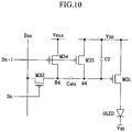
- Affichage luminescent (100) comprenant une pluralité de lignes de données (D1, ..., Dm) agencées pour transmettre des tensions de données (VDATA) correspondant à des signaux vidéo, une pluralité de lignes de balayage (S1, ..., Sn) agencées pour transmettre des signaux de sélection, et une pluralité de circuits de pixels (10), chaque circuit de pixels (10) étant couplé à une dite ligne de données correspondante (D1, ..., Dm) pour recevoir une dite tension de données correspondante (VDATA) et une dite ligne de balayage correspondante (S1, ..., Sn) pour recevoir un dit signal de sélection correspondant, chaque dit circuit de pixels (10) comprenant :un transistor (M1) comprenant une première électrode, une deuxième électrode, agencées pour recevoir une première tension d'alimentation (VDD), et une troisième électrode agencée pour délivrer en sortie un courant (IOLED) correspondant à une tension entre la première électrode et la deuxième électrode ;un élément luminescent (OLED) couplé à la troisième électrode, agencé pour émettre une lumière correspondant au courant (IOLED) délivré en sortie par la troisième électrode ;un premier commutateur (M2) agencé pour transmettre ladite tension de données correspondante (VDATA) en réponse audit signal de sélection correspondant provenant de ladite ligne de balayage correspondante (S1, ..., Sn) ; etun compensateur de tension (11) agencé pour recevoir ladite tension de données correspondante (VDATA) transmise par le premier commutateur (M2) et une deuxième tension d'alimentation (VSUS), et pour appliquer une tension de données compensée basée sur ladite tension de données correspondante (VDATA) et la deuxième tension d'alimentation (VSUS) à la première électrode du transistor (M1),dans lequel le compensateur de tension (11) comprend :un condensateur (Cst1) ayant une première électrode (A) couplée à la première électrode du transistor (M1), et une deuxième électrode (B) couplée au premier commutateur (M2); etun troisième commutateur (M4) couplé entre la deuxième électrode (B) du condensateur (Cst1) et la deuxième tension d'alimentation (VSUS), agencé pour isoler électriquement la deuxième tension d'alimentation (VSUS) vis-à-vis de la deuxième électrode (B) du condensateur (Cst1) en réponse à un deuxième signal de commande (Sn),et caractérisé en ce que le compensateur de tension (11) comprend en outre :
un deuxième commutateur (M3) agencé pour appliquer la première tension d'alimentation (VDD) à la première électrode (A) du condensateur (Cst1) en réponse à un premier signal de commande (Control signal), le deuxième commutateur (M3) consistant en un transistor ayant une électrode de grille, une première électrode et une deuxième électrode, dans lequel la première électrode du deuxième commutateur (M3) est couplée directement à la première tension d'alimentation (VDD) et la deuxième électrode du deuxième commutateur (M3) est couplée directement à la première électrode (A) du condensateur (Cst1). - Affichage luminescent (100) selon la revendication 1, dans lequel les premier et deuxième commutateurs (M2, M3) comprennent des transistors ayant un même type de canal, et le premier signal de commande (Control signal) est ledit signal de sélection correspondant provenant de ladite ligne de balayage correspondante (S1, ..., Sn) ou un autre signal qui a les mêmes caractéristiques que ledit signal de sélection correspondant provenant de ladite ligne de balayage correspondante (S1, ..., Sn).
- Affichage luminescent (100) selon la revendication 1, dans lequel le troisième commutateur (M4) comprend un transistor ayant un type de canal qui est différent de celui du premier commutateur (M2), et le deuxième signal de commande est ledit signal de sélection correspondant provenant de ladite ligne de balayage correspondante (S1, ..., Sn) ou un autre signal qui a les mêmes caractéristiques que ledit signal de sélection correspondant provenant de ladite ligne de balayage correspondante (S1, ..., Sn).
- Affichage luminescent (100) selon la revendication 1, dans lequel le compensateur de tension (11) est adapté pour fournir une tension de données compensée correspondant à une tension obtenue par soustraction de ladite tension de données correspondante (VDATA) de la somme des première et deuxième tensions d'alimentation (VDD et VSUS).
- Procédé pour piloter un panneau d'affichage (100) selon l'une des revendications précédentes, le procédé comprenant :l'application de la première tension d'alimentation (VDD) à la première électrode (A) du condensateur (Cst1) par l'intermédiaire du deuxième commutateur (M3) en réponse au premier signal de commande (Control signal) ;l'application de la tension de données (VDATA) à la deuxième électrode (B) du condensateur (Cst1) par l'intermédiaire du premier commutateur (M2) ;l'isolation électrique de la première électrode (A) du condensateur (Cst1) vis-à-vis de la première tension d'alimentation (VDD) ; etl'application de la deuxième tension d'alimentation (VSUS) à la deuxième électrode (B) du condensateur (Cst1).
- Procédé selon la revendication 5, dans lequel le transistor (M1) a un canal de type P, et la première tension d'alimentation (VDD) appliquée à la deuxième électrode du transistor (M1) est une tension positive.
- Procédé selon la revendication 5, dans lequel la deuxième tension d'alimentation (VSUS) appliquée à la deuxième électrode (B) du condensateur (Cst1) est inférieure à la somme de la tension de données (VDATA) et d'une tension de seuil du transistor (M1).
Applications Claiming Priority (2)
| Application Number | Priority Date | Filing Date | Title |
|---|---|---|---|
| KR1020030085067A KR100599726B1 (ko) | 2003-11-27 | 2003-11-27 | 발광 표시 장치 및 그 표시 패널과 구동 방법 |
| KR2003085067 | 2003-11-27 |
Publications (3)
| Publication Number | Publication Date |
|---|---|
| EP1536405A2 EP1536405A2 (fr) | 2005-06-01 |
| EP1536405A3 EP1536405A3 (fr) | 2006-05-03 |
| EP1536405B1 true EP1536405B1 (fr) | 2018-12-12 |
Family
ID=34464759
Family Applications (1)
| Application Number | Title | Priority Date | Filing Date |
|---|---|---|---|
| EP04090384.1A Active EP1536405B1 (fr) | 2003-11-27 | 2004-10-06 | Dispositif d'affichage électroluminescent, panneau d'affichage, et sa méthode de commande |
Country Status (5)
| Country | Link |
|---|---|
| US (2) | US7940233B2 (fr) |
| EP (1) | EP1536405B1 (fr) |
| JP (3) | JP4786135B2 (fr) |
| KR (1) | KR100599726B1 (fr) |
| CN (2) | CN100399393C (fr) |
Families Citing this family (104)
| Publication number | Priority date | Publication date | Assignee | Title |
|---|---|---|---|---|
| JP4033166B2 (ja) * | 2004-04-22 | 2008-01-16 | セイコーエプソン株式会社 | 電子回路、その駆動方法、電気光学装置および電子機器 |
| KR100698681B1 (ko) * | 2004-06-29 | 2007-03-23 | 삼성에스디아이 주식회사 | 발광 표시장치 |
| US7616177B2 (en) * | 2004-08-02 | 2009-11-10 | Tpo Displays Corp. | Pixel driving circuit with threshold voltage compensation |
| KR100604057B1 (ko) * | 2004-09-24 | 2006-07-24 | 삼성에스디아이 주식회사 | 화소 및 이를 이용한 발광 표시장치 |
| KR100592636B1 (ko) * | 2004-10-08 | 2006-06-26 | 삼성에스디아이 주식회사 | 발광표시장치 |
| KR20060054603A (ko) * | 2004-11-15 | 2006-05-23 | 삼성전자주식회사 | 표시 장치 및 그 구동 방법 |
| CA2490858A1 (fr) | 2004-12-07 | 2006-06-07 | Ignis Innovation Inc. | Methode d'attaque pour la programmation a tension compensee d'affichages del organiques a matrice active |
| JP2006215296A (ja) * | 2005-02-04 | 2006-08-17 | Sony Corp | 表示装置、画素駆動方法 |
| KR101152119B1 (ko) * | 2005-02-07 | 2012-06-15 | 삼성전자주식회사 | 표시 장치 및 그 구동 방법 |
| JP4752315B2 (ja) * | 2005-04-19 | 2011-08-17 | セイコーエプソン株式会社 | 電子回路、その駆動方法、電気光学装置および電子機器 |
| KR101186877B1 (ko) * | 2005-04-22 | 2012-10-02 | 엘지디스플레이 주식회사 | 휘도 조절판 및 이를 포함하는 유기 이엘 패널 |
| JP4826131B2 (ja) * | 2005-04-28 | 2011-11-30 | セイコーエプソン株式会社 | 発光装置および電子機器 |
| CN102663977B (zh) | 2005-06-08 | 2015-11-18 | 伊格尼斯创新有限公司 | 用于驱动发光器件显示器的方法和系统 |
| KR100624314B1 (ko) | 2005-06-22 | 2006-09-19 | 삼성에스디아이 주식회사 | 발광표시장치 및 박막트랜지스터 |
| US8629819B2 (en) * | 2005-07-14 | 2014-01-14 | Semiconductor Energy Laboratory Co., Ltd. | Semiconductor device and driving method thereof |
| KR101324756B1 (ko) * | 2005-10-18 | 2013-11-05 | 가부시키가이샤 한도오따이 에네루기 켄큐쇼 | 표시장치 및 그의 구동방법 |
| JP5013697B2 (ja) * | 2005-10-19 | 2012-08-29 | 三洋電機株式会社 | 表示装置 |
| KR100732828B1 (ko) | 2005-11-09 | 2007-06-27 | 삼성에스디아이 주식회사 | 화소 및 이를 이용한 발광 표시장치 |
| FR2895131A1 (fr) * | 2005-12-20 | 2007-06-22 | Thomson Licensing Sas | Panneau d'affichage et procede de pilotage avec couplage capacitif transitoire |
| US7545348B2 (en) * | 2006-01-04 | 2009-06-09 | Tpo Displays Corp. | Pixel unit and display and electronic device utilizing the same |
| US9489891B2 (en) | 2006-01-09 | 2016-11-08 | Ignis Innovation Inc. | Method and system for driving an active matrix display circuit |
| TWI371018B (en) | 2006-05-09 | 2012-08-21 | Chimei Innolux Corp | System for displaying image and driving display element method |
| EP1857998A1 (fr) * | 2006-05-19 | 2007-11-21 | TPO Displays Corp. | Système d'affichage d'image et commande du procédé d'affichage de l'élément |
| JP4203770B2 (ja) | 2006-05-29 | 2009-01-07 | ソニー株式会社 | 画像表示装置 |
| US8325118B2 (en) | 2006-05-30 | 2012-12-04 | Sharp Kabushiki Kaisha | Electric current driving type display device |
| JP2007323036A (ja) | 2006-06-05 | 2007-12-13 | Samsung Sdi Co Ltd | 有機電界発光表示装置及びその駆動方法 |
| KR100793557B1 (ko) | 2006-06-05 | 2008-01-14 | 삼성에스디아이 주식회사 | 유기전계발광표시장치 및 그의 구동방법 |
| JP4314638B2 (ja) * | 2006-08-01 | 2009-08-19 | カシオ計算機株式会社 | 表示装置及びその駆動制御方法 |
| KR100739334B1 (ko) * | 2006-08-08 | 2007-07-12 | 삼성에스디아이 주식회사 | 화소와 이를 이용한 유기전계발광 표시장치 및 그의구동방법 |
| KR100812003B1 (ko) * | 2006-08-08 | 2008-03-10 | 삼성에스디아이 주식회사 | 유기전계발광 표시장치 |
| TWI340370B (en) * | 2006-08-24 | 2011-04-11 | Chimei Innolux Corp | System for displaying image |
| TWI442368B (zh) * | 2006-10-26 | 2014-06-21 | Semiconductor Energy Lab | 電子裝置,顯示裝置,和半導體裝置,以及其驅動方法 |
| KR100815756B1 (ko) * | 2006-11-14 | 2008-03-20 | 삼성에스디아이 주식회사 | 화소 및 이를 이용한 유기전계발광 표시장치 및 그의구동방법 |
| JP4887203B2 (ja) | 2006-11-14 | 2012-02-29 | 三星モバイルディスプレイ株式會社 | 画素、有機電界発光表示装置、および有機電界発光表示装置の駆動方法 |
| KR101373736B1 (ko) * | 2006-12-27 | 2014-03-14 | 삼성디스플레이 주식회사 | 표시 장치 및 그 구동 방법 |
| US20080165171A1 (en) * | 2007-01-09 | 2008-07-10 | Himax Technologies Limited | Display Driving Circuit and Method Thereof |
| KR100853540B1 (ko) * | 2007-02-01 | 2008-08-21 | 삼성에스디아이 주식회사 | 유기전계발광표시장치 및 그의 에이징 방법 |
| KR100873074B1 (ko) * | 2007-03-02 | 2008-12-09 | 삼성모바일디스플레이주식회사 | 화소 및 이를 이용한 유기전계발광 표시장치 및 그의구동방법 |
| KR101341788B1 (ko) * | 2007-07-09 | 2013-12-13 | 엘지디스플레이 주식회사 | 발광 표시장치 및 그의 구동방법 |
| KR100926591B1 (ko) * | 2007-07-23 | 2009-11-11 | 재단법인서울대학교산학협력재단 | 유기 전계 발광 표시 장치 |
| JP5148951B2 (ja) * | 2007-08-30 | 2013-02-20 | エルジー ディスプレイ カンパニー リミテッド | 画像表示装置、および画像表示装置の駆動方法 |
| JP4979772B2 (ja) | 2007-10-18 | 2012-07-18 | シャープ株式会社 | 電流駆動型表示装置 |
| KR101429711B1 (ko) * | 2007-11-06 | 2014-08-13 | 삼성디스플레이 주식회사 | 유기 발광 표시 장치 및 그것의 구동 방법 |
| KR101416904B1 (ko) * | 2007-11-07 | 2014-07-09 | 엘지디스플레이 주식회사 | 유기전계발광 표시장치의 화소 구동 장치 |
| KR100931469B1 (ko) * | 2008-02-28 | 2009-12-11 | 삼성모바일디스플레이주식회사 | 화소 및 이를 이용한 유기전계발광 표시장치 |
| KR100911981B1 (ko) * | 2008-03-04 | 2009-08-13 | 삼성모바일디스플레이주식회사 | 화소 및 이를 이용한 유기전계발광 표시장치 |
| KR100922071B1 (ko) | 2008-03-10 | 2009-10-16 | 삼성모바일디스플레이주식회사 | 화소 및 이를 이용한 유기전계발광 표시장치 |
| WO2009127065A1 (fr) | 2008-04-18 | 2009-10-22 | Ignis Innovation Inc. | Système et procédé de commande d'un affichage par dispositif électroluminescent |
| US20100007651A1 (en) * | 2008-07-08 | 2010-01-14 | Yang-Wan Kim | Pixel and organic light emitting display using the same |
| US9370075B2 (en) | 2008-12-09 | 2016-06-14 | Ignis Innovation Inc. | System and method for fast compensation programming of pixels in a display |
| JP2010164844A (ja) * | 2009-01-16 | 2010-07-29 | Nec Lcd Technologies Ltd | 液晶表示装置、該液晶表示装置に用いられる駆動方法及び集積回路 |
| JP5299126B2 (ja) * | 2009-07-01 | 2013-09-25 | セイコーエプソン株式会社 | 発光装置および電子機器、並びに画素回路の駆動方法。 |
| KR101056281B1 (ko) | 2009-08-03 | 2011-08-11 | 삼성모바일디스플레이주식회사 | 유기 전계발광 표시장치 및 그의 구동방법 |
| KR20110013693A (ko) * | 2009-08-03 | 2011-02-10 | 삼성모바일디스플레이주식회사 | 유기 전계발광 표시장치 및 그의 구동방법 |
| JP2011145481A (ja) * | 2010-01-14 | 2011-07-28 | Sony Corp | 表示装置、表示駆動方法 |
| KR101074814B1 (ko) * | 2010-02-02 | 2011-10-19 | 삼성모바일디스플레이주식회사 | 디스플레이 장치 및 그 구동 방법 |
| KR101142729B1 (ko) * | 2010-03-17 | 2012-05-03 | 삼성모바일디스플레이주식회사 | 화소 및 이를 이용한 유기전계발광 표시장치 |
| KR101645404B1 (ko) * | 2010-07-06 | 2016-08-04 | 삼성디스플레이 주식회사 | 유기 전계발광 표시장치 |
| TWI433111B (zh) * | 2010-12-22 | 2014-04-01 | Univ Nat Taiwan Science Tech | 有機發光二極體的畫素單元及具有其之顯示面板 |
| KR20120111675A (ko) * | 2011-04-01 | 2012-10-10 | 삼성디스플레이 주식회사 | 유기발광 표시 장치, 유기발광 표시 장치를 위한 데이터 구동 장치 및 그 구동 방법 |
| KR101186637B1 (ko) * | 2011-05-02 | 2012-09-27 | 한양대학교 산학협력단 | 화소 및 이를 이용한 유기전계발광 표시장치 |
| US9886899B2 (en) | 2011-05-17 | 2018-02-06 | Ignis Innovation Inc. | Pixel Circuits for AMOLED displays |
| US9351368B2 (en) | 2013-03-08 | 2016-05-24 | Ignis Innovation Inc. | Pixel circuits for AMOLED displays |
| US20140368491A1 (en) | 2013-03-08 | 2014-12-18 | Ignis Innovation Inc. | Pixel circuits for amoled displays |
| CN106898307B (zh) | 2011-05-28 | 2021-04-27 | 伊格尼斯创新公司 | 在以交错模式实施的显示器上显示图像的方法 |
| CN102654972B (zh) * | 2011-06-21 | 2015-08-12 | 京东方科技集团股份有限公司 | 有源矩阵有机发光二极体面板及其驱动电路与方法 |
| JP6050054B2 (ja) | 2011-09-09 | 2016-12-21 | 株式会社半導体エネルギー研究所 | 半導体装置 |
| TW201313070A (zh) * | 2011-09-13 | 2013-03-16 | Wintek Corp | 發光元件驅動電路及其相關的畫素電路與應用 |
| TW201314660A (zh) * | 2011-09-19 | 2013-04-01 | Wintek Corp | 發光元件驅動電路及其相關的畫素電路與應用 |
| CN102651197A (zh) * | 2011-11-01 | 2012-08-29 | 京东方科技集团股份有限公司 | 有机发光二极管驱动电路、显示面板、显示器及驱动方法 |
| US9095031B2 (en) | 2011-11-01 | 2015-07-28 | Boe Technology Group Co., Ltd. | Organic light emitting diode driving circuit, display panel, display and driving method |
| CN102654976B (zh) * | 2012-01-12 | 2014-12-24 | 京东方科技集团股份有限公司 | 一种像素电路及其驱动方法、显示装置 |
| CN102456319A (zh) * | 2012-02-15 | 2012-05-16 | 福州华映视讯有限公司 | 画素电路及其驱动方法 |
| US10043794B2 (en) | 2012-03-22 | 2018-08-07 | Semiconductor Energy Laboratory Co., Ltd. | Semiconductor device and electronic device |
| US9747834B2 (en) | 2012-05-11 | 2017-08-29 | Ignis Innovation Inc. | Pixel circuits including feedback capacitors and reset capacitors, and display systems therefore |
| TWI462080B (zh) * | 2012-08-14 | 2014-11-21 | Au Optronics Corp | 主動式有機發光二極體電路及其操作方法 |
| KR102084288B1 (ko) * | 2012-11-05 | 2020-03-03 | 유니버시티 오브 플로리다 리서치 파운데이션, 아이엔씨. | 디스플레이의 휘도 보상 |
| US9786223B2 (en) | 2012-12-11 | 2017-10-10 | Ignis Innovation Inc. | Pixel circuits for AMOLED displays |
| US9336717B2 (en) | 2012-12-11 | 2016-05-10 | Ignis Innovation Inc. | Pixel circuits for AMOLED displays |
| CA2894717A1 (fr) | 2015-06-19 | 2016-12-19 | Ignis Innovation Inc. | Caracterisation d'un dispositif optoelectronique au moyen d'une ligne de sens partage |
| US9721505B2 (en) | 2013-03-08 | 2017-08-01 | Ignis Innovation Inc. | Pixel circuits for AMOLED displays |
| CN104537984B (zh) * | 2013-05-21 | 2017-05-03 | 京东方科技集团股份有限公司 | 一种像素电路及其驱动方法 |
| CN104157234A (zh) * | 2014-01-17 | 2014-11-19 | 北京京东方光电科技有限公司 | 像素单元驱动电路及方法、显示装置 |
| CN110264955A (zh) * | 2014-06-06 | 2019-09-20 | 伊格尼斯创新公司 | 显示器系统、控制显示器的系统和电路元件特性的确定方法 |
| KR20160000980A (ko) | 2014-06-25 | 2016-01-06 | 삼성디스플레이 주식회사 | 디스플레이 장치 |
| CN104318897B (zh) * | 2014-11-13 | 2017-06-06 | 合肥鑫晟光电科技有限公司 | 一种像素电路、有机电致发光显示面板及显示装置 |
| CA2873476A1 (fr) | 2014-12-08 | 2016-06-08 | Ignis Innovation Inc. | Architecture d'affichage de pixels intelligents |
| CN104778917B (zh) * | 2015-01-30 | 2017-12-19 | 京东方科技集团股份有限公司 | 像素驱动电路及其驱动方法和显示设备 |
| KR102420461B1 (ko) | 2015-02-06 | 2022-07-14 | 삼성디스플레이 주식회사 | 디스플레이 장치 및 이의 제조 방법 |
| CN104715724B (zh) * | 2015-03-25 | 2017-05-24 | 北京大学深圳研究生院 | 像素电路及其驱动方法和一种显示装置 |
| CA2886862A1 (fr) | 2015-04-01 | 2016-10-01 | Ignis Innovation Inc. | Ajustement de la luminosite d'affichage en vue d'eviter la surchauffe ou le vieillissement accelere |
| US10657895B2 (en) | 2015-07-24 | 2020-05-19 | Ignis Innovation Inc. | Pixels and reference circuits and timing techniques |
| US10373554B2 (en) | 2015-07-24 | 2019-08-06 | Ignis Innovation Inc. | Pixels and reference circuits and timing techniques |
| CA2898282A1 (fr) | 2015-07-24 | 2017-01-24 | Ignis Innovation Inc. | Etalonnage hybride de sources de courant destine a des afficheurs a tension polarisee par courant programmes |
| KR102412468B1 (ko) | 2015-08-11 | 2022-06-23 | 삼성디스플레이 주식회사 | 표시 장치 |
| CA2908285A1 (fr) | 2015-10-14 | 2017-04-14 | Ignis Innovation Inc. | Pilote comportant une structure de pixel a plusieurs couleurs |
| CN106782313B (zh) * | 2016-12-15 | 2019-04-12 | 上海天马有机发光显示技术有限公司 | 有机发光像素驱动电路、驱动方法及有机发光显示面板 |
| CN106782331B (zh) * | 2016-12-27 | 2023-07-18 | 京东方科技集团股份有限公司 | 一种像素电路、其驱动方法、显示面板及显示装置 |
| KR102312348B1 (ko) * | 2017-06-30 | 2021-10-13 | 엘지디스플레이 주식회사 | 표시패널과 이를 이용한 전계 발광 표시장치 |
| WO2020050827A1 (fr) * | 2018-09-05 | 2020-03-12 | Hewlett-Packard Development Company, L.P. | Circuits oled à huit transistors/1 condensateurs |
| KR102051102B1 (ko) * | 2018-12-12 | 2019-12-03 | 삼성디스플레이 주식회사 | 화소 |
| CN113539171A (zh) * | 2021-07-27 | 2021-10-22 | 深圳市华星光电半导体显示技术有限公司 | 显示像素电路、显示像素电路驱动方法及显示面板 |
| KR20230120164A (ko) | 2022-02-07 | 2023-08-17 | 삼성디스플레이 주식회사 | 화소 회로 및 이를 포함하는 표시 장치 |
| CN115410530B (zh) * | 2022-08-30 | 2023-07-18 | 惠科股份有限公司 | 像素补偿电路、驱动方法和显示面板 |
Family Cites Families (41)
| Publication number | Priority date | Publication date | Assignee | Title |
|---|---|---|---|---|
| US5952789A (en) | 1997-04-14 | 1999-09-14 | Sarnoff Corporation | Active matrix organic light emitting diode (amoled) display pixel structure and data load/illuminate circuit therefor |
| US6229506B1 (en) | 1997-04-23 | 2001-05-08 | Sarnoff Corporation | Active matrix light emitting diode pixel structure and concomitant method |
| GB9812742D0 (en) | 1998-06-12 | 1998-08-12 | Philips Electronics Nv | Active matrix electroluminescent display devices |
| US6384804B1 (en) | 1998-11-25 | 2002-05-07 | Lucent Techonologies Inc. | Display comprising organic smart pixels |
| KR100284341B1 (ko) * | 1999-03-02 | 2001-03-02 | 김순택 | Ac형 플라즈마 표시 패널의 구동 방법 |
| GB0008019D0 (en) | 2000-03-31 | 2000-05-17 | Koninkl Philips Electronics Nv | Display device having current-addressed pixels |
| WO2002005255A1 (fr) | 2000-07-07 | 2002-01-17 | Seiko Epson Corporation | Dispositif electrooptique d'attaque de courant tel qu'un afficheur electroluminescent organique, avec des transistors d'attaque complementaires destines a contrecarrer les variation de la tension de seuil |
| KR100370286B1 (ko) | 2000-12-29 | 2003-01-29 | 삼성에스디아이 주식회사 | 전압구동 유기발광소자의 픽셀회로 |
| TW561445B (en) * | 2001-01-02 | 2003-11-11 | Chi Mei Optoelectronics Corp | OLED active driving system with current feedback |
| KR100370095B1 (ko) | 2001-01-05 | 2003-02-05 | 엘지전자 주식회사 | 표시 소자의 액티브 매트릭스 방식의 구동 회로 |
| US7061451B2 (en) | 2001-02-21 | 2006-06-13 | Semiconductor Energy Laboratory Co., Ltd, | Light emitting device and electronic device |
| WO2002075710A1 (fr) | 2001-03-21 | 2002-09-26 | Canon Kabushiki Kaisha | Circuit de commande d'un element lumineux a matrice active |
| JP2002351401A (ja) | 2001-03-21 | 2002-12-06 | Mitsubishi Electric Corp | 自発光型表示装置 |
| WO2002075709A1 (fr) | 2001-03-21 | 2002-09-26 | Canon Kabushiki Kaisha | Circuit permettant d'actionner un element electroluminescent a matrice active |
| SG119161A1 (en) | 2001-07-16 | 2006-02-28 | Semiconductor Energy Lab | Light emitting device |
| US7209101B2 (en) | 2001-08-29 | 2007-04-24 | Nec Corporation | Current load device and method for driving the same |
| JP4230744B2 (ja) * | 2001-09-29 | 2009-02-25 | 東芝松下ディスプレイテクノロジー株式会社 | 表示装置 |
| JP3899886B2 (ja) | 2001-10-10 | 2007-03-28 | 株式会社日立製作所 | 画像表示装置 |
| US7365713B2 (en) * | 2001-10-24 | 2008-04-29 | Semiconductor Energy Laboratory Co., Ltd. | Semiconductor device and driving method thereof |
| JP3732477B2 (ja) | 2001-10-26 | 2006-01-05 | 株式会社半導体エネルギー研究所 | 画素回路、発光装置および電子機器 |
| JP2003150107A (ja) | 2001-11-09 | 2003-05-23 | Sharp Corp | 表示装置およびその駆動方法 |
| JP2003195806A (ja) | 2001-12-06 | 2003-07-09 | Pioneer Electronic Corp | 有機エレクトロルミネッセンス素子の発光回路及び表示装置 |
| JP3800404B2 (ja) * | 2001-12-19 | 2006-07-26 | 株式会社日立製作所 | 画像表示装置 |
| US6847171B2 (en) * | 2001-12-21 | 2005-01-25 | Seiko Epson Corporation | Organic electroluminescent device compensated pixel driver circuit |
| JP2003195809A (ja) * | 2001-12-28 | 2003-07-09 | Matsushita Electric Ind Co Ltd | El表示装置とその駆動方法および情報表示装置 |
| JP3956347B2 (ja) | 2002-02-26 | 2007-08-08 | インターナショナル・ビジネス・マシーンズ・コーポレーション | ディスプレイ装置 |
| KR100649243B1 (ko) | 2002-03-21 | 2006-11-24 | 삼성에스디아이 주식회사 | 유기 전계발광 표시 장치 및 그 구동 방법 |
| JP2004054238A (ja) | 2002-05-31 | 2004-02-19 | Seiko Epson Corp | 電子回路、電気光学装置、電気光学装置の駆動方法、及び電子機器 |
| KR100432651B1 (ko) | 2002-06-18 | 2004-05-22 | 삼성에스디아이 주식회사 | 화상 표시 장치 |
| JP4123084B2 (ja) | 2002-07-31 | 2008-07-23 | セイコーエプソン株式会社 | 電子回路、電気光学装置、及び電子機器 |
| KR20040019207A (ko) | 2002-08-27 | 2004-03-05 | 엘지.필립스 엘시디 주식회사 | 유기전계발광소자와 그의 구동장치 및 방법 |
| JP4144462B2 (ja) | 2002-08-30 | 2008-09-03 | セイコーエプソン株式会社 | 電気光学装置及び電子機器 |
| JP2004145278A (ja) | 2002-08-30 | 2004-05-20 | Seiko Epson Corp | 電子回路、電子回路の駆動方法、電気光学装置、電気光学装置の駆動方法及び電子機器 |
| KR100450761B1 (ko) | 2002-09-14 | 2004-10-01 | 한국전자통신연구원 | 능동 구동형 유기 이엘 다이오드 디스플레이 패널 회로 |
| JP2004145300A (ja) | 2002-10-03 | 2004-05-20 | Seiko Epson Corp | 電子回路、電子回路の駆動方法、電子装置、電気光学装置、電気光学装置の駆動方法及び電子機器 |
| JP3832415B2 (ja) * | 2002-10-11 | 2006-10-11 | ソニー株式会社 | アクティブマトリクス型表示装置 |
| JP4734529B2 (ja) | 2003-02-24 | 2011-07-27 | 奇美電子股▲ふん▼有限公司 | 表示装置 |
| JP2004286816A (ja) * | 2003-03-19 | 2004-10-14 | Toshiba Matsushita Display Technology Co Ltd | アクティブマトリクス型表示装置及びその駆動方法 |
| US20040222954A1 (en) * | 2003-04-07 | 2004-11-11 | Lueder Ernst H. | Methods and apparatus for a display |
| JP4062179B2 (ja) * | 2003-06-04 | 2008-03-19 | ソニー株式会社 | 画素回路、表示装置、および画素回路の駆動方法 |
| JP4297438B2 (ja) * | 2003-11-24 | 2009-07-15 | 三星モバイルディスプレイ株式會社 | 発光表示装置,表示パネル,及び発光表示装置の駆動方法 |
-
2003
- 2003-11-27 KR KR1020030085067A patent/KR100599726B1/ko active IP Right Grant
-
2004
- 2004-02-26 JP JP2004051968A patent/JP4786135B2/ja not_active Expired - Lifetime
- 2004-08-16 US US10/919,693 patent/US7940233B2/en active Active
- 2004-10-06 EP EP04090384.1A patent/EP1536405B1/fr active Active
- 2004-10-14 CN CNB2004100881689A patent/CN100399393C/zh active Active
- 2004-10-14 CN CN2007101489867A patent/CN101136174B/zh active Active
-
2009
- 2009-09-16 JP JP2009214825A patent/JP4786737B2/ja not_active Expired - Lifetime
-
2010
- 2010-09-27 JP JP2010215206A patent/JP5324543B2/ja not_active Expired - Lifetime
-
2011
- 2011-05-06 US US13/103,000 patent/US8717258B2/en active Active
Non-Patent Citations (1)
| Title |
|---|
| None * |
Also Published As
| Publication number | Publication date |
|---|---|
| KR20050051300A (ko) | 2005-06-01 |
| US20050140600A1 (en) | 2005-06-30 |
| CN101136174A (zh) | 2008-03-05 |
| EP1536405A2 (fr) | 2005-06-01 |
| US20110210990A1 (en) | 2011-09-01 |
| JP2005157244A (ja) | 2005-06-16 |
| CN1622168A (zh) | 2005-06-01 |
| JP5324543B2 (ja) | 2013-10-23 |
| KR100599726B1 (ko) | 2006-07-12 |
| JP4786135B2 (ja) | 2011-10-05 |
| US7940233B2 (en) | 2011-05-10 |
| JP2009294674A (ja) | 2009-12-17 |
| CN101136174B (zh) | 2011-04-06 |
| US8717258B2 (en) | 2014-05-06 |
| CN100399393C (zh) | 2008-07-02 |
| JP2011043837A (ja) | 2011-03-03 |
| EP1536405A3 (fr) | 2006-05-03 |
| JP4786737B2 (ja) | 2011-10-05 |
Similar Documents
| Publication | Publication Date | Title |
|---|---|---|
| EP1536405B1 (fr) | Dispositif d'affichage électroluminescent, panneau d'affichage, et sa méthode de commande | |
| US6919871B2 (en) | Light emitting display, display panel, and driving method thereof | |
| EP1465141B1 (fr) | Affichage émettant de la lumière, panneau d' affichage et sa méthode de commande | |
| US7446740B2 (en) | Image display device and driving method thereof | |
| EP1585100B1 (fr) | Dispositif d'affichage électroluminescent et circuit de commande de pixel approprié | |
| EP1465142B1 (fr) | Affichage émettant de la lumière, panneau d'affichage et sa méthode de commande | |
| US7365742B2 (en) | Light emitting display and driving method thereof | |
| EP1473689B1 (fr) | Circuit pixel, panneau d'affichage, dispositif d'affichage et procédé de commande pour ceux-ci | |
| US7489290B2 (en) | Light emitting display device and driving method thereof | |
| US7167406B2 (en) | Image display device and driving method thereof | |
| US7109982B2 (en) | Display panel and driving method thereof | |
| US20050110721A1 (en) | Display panel, light emitting display device using the same, and driving method thereof | |
| KR100515307B1 (ko) | 화상 표시 장치 및 그 구동 방법 |
Legal Events
| Date | Code | Title | Description |
|---|---|---|---|
| PUAI | Public reference made under article 153(3) epc to a published international application that has entered the european phase |
Free format text: ORIGINAL CODE: 0009012 |
|
| AK | Designated contracting states |
Kind code of ref document: A2 Designated state(s): AT BE BG CH CY CZ DE DK EE ES FI FR GB GR HU IE IT LI LU MC NL PL PT RO SE SI SK TR |
|
| AX | Request for extension of the european patent |
Extension state: AL HR LT LV MK |
|
| PUAL | Search report despatched |
Free format text: ORIGINAL CODE: 0009013 |
|
| AK | Designated contracting states |
Kind code of ref document: A3 Designated state(s): AT BE BG CH CY CZ DE DK EE ES FI FR GB GR HU IE IT LI LU MC NL PL PT RO SE SI SK TR |
|
| AX | Request for extension of the european patent |
Extension state: AL HR LT LV MK |
|
| 17P | Request for examination filed |
Effective date: 20061103 |
|
| AKX | Designation fees paid |
Designated state(s): DE FR GB |
|
| 17Q | First examination report despatched |
Effective date: 20071121 |
|
| RAP1 | Party data changed (applicant data changed or rights of an application transferred) |
Owner name: SAMSUNG MOBILE DISPLAY CO., LTD. |
|
| RAP1 | Party data changed (applicant data changed or rights of an application transferred) |
Owner name: SAMSUNG DISPLAY CO., LTD. |
|
| RAP1 | Party data changed (applicant data changed or rights of an application transferred) |
Owner name: SAMSUNG DISPLAY CO., LTD. |
|
| GRAP | Despatch of communication of intention to grant a patent |
Free format text: ORIGINAL CODE: EPIDOSNIGR1 |
|
| INTG | Intention to grant announced |
Effective date: 20180425 |
|
| GRAS | Grant fee paid |
Free format text: ORIGINAL CODE: EPIDOSNIGR3 |
|
| GRAA | (expected) grant |
Free format text: ORIGINAL CODE: 0009210 |
|
| AK | Designated contracting states |
Kind code of ref document: B1 Designated state(s): DE FR GB |
|
| REG | Reference to a national code |
Ref country code: GB Ref legal event code: FG4D |
|
| REG | Reference to a national code |
Ref country code: DE Ref legal event code: R096 Ref document number: 602004053535 Country of ref document: DE |
|
| REG | Reference to a national code |
Ref country code: DE Ref legal event code: R097 Ref document number: 602004053535 Country of ref document: DE |
|
| PLBE | No opposition filed within time limit |
Free format text: ORIGINAL CODE: 0009261 |
|
| STAA | Information on the status of an ep patent application or granted ep patent |
Free format text: STATUS: NO OPPOSITION FILED WITHIN TIME LIMIT |
|
| 26N | No opposition filed |
Effective date: 20190913 |
|
| P01 | Opt-out of the competence of the unified patent court (upc) registered |
Effective date: 20230515 |
|
| PGFP | Annual fee paid to national office [announced via postgrant information from national office to epo] |
Ref country code: GB Payment date: 20230920 Year of fee payment: 20 |
|
| PGFP | Annual fee paid to national office [announced via postgrant information from national office to epo] |
Ref country code: FR Payment date: 20230922 Year of fee payment: 20 |
|
| PGFP | Annual fee paid to national office [announced via postgrant information from national office to epo] |
Ref country code: DE Payment date: 20230920 Year of fee payment: 20 |