EP1533897A2 - Filter mit piezoelektrischem Resonator - Google Patents
Filter mit piezoelektrischem Resonator Download PDFInfo
- Publication number
- EP1533897A2 EP1533897A2 EP04026155A EP04026155A EP1533897A2 EP 1533897 A2 EP1533897 A2 EP 1533897A2 EP 04026155 A EP04026155 A EP 04026155A EP 04026155 A EP04026155 A EP 04026155A EP 1533897 A2 EP1533897 A2 EP 1533897A2
- Authority
- EP
- European Patent Office
- Prior art keywords
- electrode
- piezoelectric resonator
- series
- parallel
- piezoelectric
- Prior art date
- Legal status (The legal status is an assumption and is not a legal conclusion. Google has not performed a legal analysis and makes no representation as to the accuracy of the status listed.)
- Withdrawn
Links
Images


Classifications
-
- H—ELECTRICITY
- H03—ELECTRONIC CIRCUITRY
- H03H—IMPEDANCE NETWORKS, e.g. RESONANT CIRCUITS; RESONATORS
- H03H9/00—Networks comprising electromechanical or electro-acoustic elements; Electromechanical resonators
- H03H9/46—Filters
- H03H9/54—Filters comprising resonators of piezoelectric or electrostrictive material
- H03H9/58—Multiple crystal filters
- H03H9/60—Electric coupling means therefor
- H03H9/605—Electric coupling means therefor consisting of a ladder configuration
-
- H—ELECTRICITY
- H03—ELECTRONIC CIRCUITRY
- H03H—IMPEDANCE NETWORKS, e.g. RESONANT CIRCUITS; RESONATORS
- H03H9/00—Networks comprising electromechanical or electro-acoustic elements; Electromechanical resonators
- H03H9/46—Filters
- H03H9/64—Filters using surface acoustic waves
- H03H9/6423—Means for obtaining a particular transfer characteristic
- H03H9/6433—Coupled resonator filters
Definitions
- the present invention relates to a filter using piezoelectric resonators, and in particular to a filter using piezoelectric resonators to be used in wireless circuits of mobile communication terminals such as mobile phones and wireless LANs.
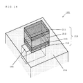
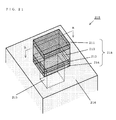
- FIG. 21 is a perspective view showing the basic structure of a piezoelectric resonator.
- FIG. 22 is a cross-sectional view taken along line B-B of FIG. 21.
- FIG. 23A is a diagram showing a circuit symbol of the piezoelectric resonator and
- FIG. 23B is an equivalent circuit diagram of the piezoelectric resonator.
- FIG. 24 is a diagram showing the frequency characteristics of the piezoelectric resonator.
- a piezoelectric resonator 210 is constructed such that an upper electrode layer 211, a piezoelectric material layer 212, a lower electrode layer 213, an insulating material layer 214, and a cavity 215 are formed on/in a substrate 216 such as silicon or glass.
- the cavity 215 is provided in the substrate 216 so as not to penetrate through the substrate 216.
- the insulating material layer 214 made of silicon dioxide (SiO 2 ), silicon nitride (Si 3 N 4 ), or the like is formed on the substrate 216 so as to cover the cavity 215.
- the lower electrode layer 213 made of molybdenum (MO) , aluminum (A1) , silver (Ag) , tungsten (W) , platinum (Pt), or the like.
- the piezoelectric material layer 212 made of aluminum nitride (AlN), zinc oxide (ZnO), lithium niobate (LiNbO 3 ), lithium tantalite (LiTaO 3 ), potassium niobate (KNbO 3 ), or the like.
- the upper electrode layer 211 made of the same material as the lower electrode layer 213.
- the upper electrode layer 211, the piezoelectric material layer 212, the lower electrode layer 213, and the insulating material layer 214 make up a vibrating portion 218.
- the vibrating portion 218 is supported by a supporting portion 221 of the substrate 216, as shown in FIG. 22.
- the cavity 215 is provided to trap therein a mechanical vibration generated by the piezoelectric material layer 212.
- the resonance frequency f r and anti-resonance frequency f a of the piezoelectric resonator 210 can be determined by the thickness and size of the layers of the vibrating portion 218 and parameters such as a constant of each material.
- the equivalent circuit of the piezoelectric resonator 210 shown in FIG. 23A is represented by a capacitance C 0 , an equivalent constant C 1 , an equivalent constant L 1 , as shown in FIG. 23B.
- the frequency characteristics of the piezoelectric resonator 210 are shown in FIG. 24.
- FIG. 25 is a diagram showing an exemplary circuit diagram of a conventional filter using three piezoelectric resonators having the above-described frequency characteristics.
- a conventional filter 250 includes a series piezoelectric resonator 251, parallel piezoelectric resonators 252a and 252b, and inductors 253a and 253b.
- the series piezoelectric resonator 251 is connected in series between an input terminal 255a and an output terminal 255b.
- a first electrode of the parallel piezoelectric resonator 252a is connected to a connection point between the input terminal 255a and the series piezoelectric resonator 251, and a second electrode of the parallel piezoelectric resonator 252a is connected to a first terminal of the inductor 253a.
- a first electrode of the parallel piezoelectric resonator 252b is connected to a connection point between the series piezoelectric resonator 251 and the output terminal 255b, and a second electrode of the parallel piezoelectric resonator 252b is connected to a first terminal of the inductor 253b. Second terminals of the inductors 253a and 253b are grounded.
- the conventional filter 250 having the above-described configuration has two types of frequency characteristics, i.e., the frequency characteristics of the parallel piezoelectric resonators 252a and 252b (solid line in graph (a) of FIG. 26) and the frequency characteristics of the series piezoelectric resonator 251 (dashed line in graph (a) of FIG. 26) . Therefore, by setting each parameter of the filter 250 such that an anti-resonance point 262 of the parallel piezoelectric resonators 252a and 252b substantially corresponds with a resonance point 263 of the series piezoelectric resonator 251, a filter having a passband 265, as shown in graph (b) of FIG. 26, can be realized.
- a reception filter for W-CDMA has a reception band of 2.11 to 2.17 GHz and a transmission band of 1.92 to 1.98 GHz.
- an object of the present invention is to provide a filter using piezoelectric resonators which is capable of minimizing a loss in the passband while obtaining a desired amount of attenuation in the attenuation band.
- another object of the present invention is to provide a filter using piezoelectric resonators which achieves a reduction in size by reducing the value or number of inductors necessary for the circuit.
- the filter of the present invention comprises: a series piezoelectric resonator part including at least one series piezoelectric resonator connected in series between input and output terminals; a parallel piezoelectric resonator part including at least two parallel piezoelectric resonators each having a first electrode and a second electrode, the parallel piezoelectric resonators being connected, via the first electrodes, in parallel to the series piezoelectric resonator and in a ladder configuration; an inductor part including inductors provided to at least two of the parallel piezoelectric resonators, respectively, the inductors each connecting between a ground and the second electrode of the parallel piezoelectric resonator; and an additional piezoelectric resonator part including at least one additional piezoelectric resonator which connects between any two second electrodes of the parallel piezoelectric resonators having the inductors connected
- a typical filter configuration may be such that the series piezoelectric resonator part includes a series piezoelectric resonator having a first electrode and a second electrode, and being connected in series between the input and output terminals, the parallel piezoelectric resonator part includes: a first parallel piezoelectric resonator having a first electrode and a second electrode, the first electrode being connected to the first electrode of the series piezoelectric resonator; and a second parallel piezoelectric resonator having a first electrode and a second electrode, the first electrode being connected to the second electrode of the series piezoelectric resonator, the inductor part includes: a first inductor connecting between the second electrode of the first parallel piezoelectric resonator and the ground; and a second inductor connecting between thesecond electrode ofthesecond parallelpiezoelectricresonator and the ground, and the additional piezoelectric resonator part includes an additional piezoelectric resonator connecting between the second electrode of the first parallel piezoelectric
- the series piezoelectric resonator part includes a first series piezoelectric resonator and a second series piezoelectric resonator which are connected in series between the input and output terminals, the first and second series piezoelectric resonators each having a first electrode and a second electrode
- the parallel piezoelectric resonator part includes: a first parallel piezoelectric resonator having a first electrode and a second electrode, the first electrode being connected to the first electrode of the first series piezoelectric resonator; a second parallel piezoelectric resonator having a first electrode and a second electrode, the first electrode'being connected between the second electrode of the first series piezoelectric resonator and the first electrode of the second series piezoelectric resonator; a third parallel piezoelectric resonator having a first electrode and a second electrode, the first electrode being connected to the second electrode of the second series piezoelectric resonator, the inductor part includes:
- the series piezoelectric resonator part includes a first series piezoelectric resonator, a second series piezoelectric resonator, and a third series piezoelectric resonator which are connected in series between the input and output terminals, the first, second, and third series piezoelectric resonators each having a first electrode and a second electrode
- the parallel piezoelectric resonator part includes: a first parallel piezoelectric resonator having a first electrode and a second electrode, the first electrode being connected to the first electrode of the first series piezoelectric resonator; a second parallel piezoelectric resonator having a first electrode and a second electrode, the first electrode being connected between the second electrode of the first series piezoelectric resonator and the first electrode of the second series piezoelectric resonator; a third parallel piezoelectric resonator having a first electrode and a second electrode, the first electrode being connected between the second electrode of the second electrode of the second series piez
- the series piezoelectric resonator, the parallel piezoelectric resonators, and the additional piezoelectric resonator may be thin-film acoustic wave resonators.
- the thin-film acoustic wave resonators each may include an upper electrode; a lower electrode; a piezoelectric material layer sandwiched between the upper and lower electrodes; and a cavity provided under the lower electrode.
- the thin-film acoustic wave resonators each may include an upper electrode; a lower electrode; a piezoelectric material layer sandwiched between the upper and lower electrodes; and an acoustic multilayer film provided under the lower electrode, the acoustic multilayer film being formed by alternately stacking a low impedance layer and a high impedance layer.
- connectionsbetweentheelectrodesoftheseriespiezoelectric resonator, the parallel piezoelectric resonators, and the additional piezoelectric resonator and the electrodes of their respective adjacent piezoelectric resonators in an equivalent circuit be established in the same wiring layer.
- the series piezoelectric resonator, the parallel piezoelectric resonators, and the additional piezoelectric resonator may be surface acoustic wave resonators.
- the surface acoustic wave resonators each may include a piezoelectric substrate; an interdigital transducer electrode; a reflector electrode, wherein the interdigital transducer electrode and the reflector electrode are arranged on the piezoelectric substrate so as to be close to each other with respect to a propagation direction.
- At least one additional piezoelectric resonator is inserted between any two second electrodes of the parallel piezoelectric resonators.
- the characteristic configuration provided by the present invention can be applied to any filter regardless of the number of piezoelectric resonators included in the filter, as long as the filter is of a ladder-type having three or more piezoelectric resonators which include one series piezoelectric resonator inserted in series between signal input and output terminals; and two parallel piezoelectric resonators inserted in parallel with the signal input and output terminals.
- the present invention will be described below using an example of a ladder filter having three piezoelectric resonators which include one series piezoelectric resonator and two parallel piezoelectric resonators.
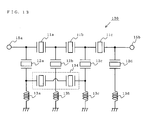
- FIG. 1 is a circuit diagram of a filter 10 using piezoelectric resonators, according to a first embodiment of the present invention.
- the filter 10 of the first embodiment includes a series piezoelectric resonator 11, parallel piezoelectric resonators 12a and 12b, inductors 13a and 13b, and an additional piezoelectric resonator 14.
- the series piezoelectric resonator 11 is connected in series between an input terminal 15a and an output terminal 15b.
- a first electrode of the parallel piezoelectric resonator 12a is connected to a connection point between the input terminal 15a and the series piezoelectric resonator 11, and a second electrode of the parallel piezoelectric resonator 12a is connected to a first terminal of the inductor 13a.
- a first electrode of the parallel piezoelectric resonator 12b is connected to a connection point between the series piezoelectric resonator 11 and the output terminal 15b, and a second electrode of the parallel piezoelectric resonator 12b is connected to a first terminal of the inductor 13b.
- Second terminals of the inductors 13a and 13b are grounded.
- the additional piezoelectric resonator 14 is connected between the second electrode of the parallel piezoelectric resonator 12a and the second electrode of the parallel piezoelectric resonator 12b.
- an equivalent circuit of a series network shown in FIG. 2 is added to the conventional circuit shown in FIG. 25.
- the resonance frequency f r and anti-resonance frequency f a of the equivalent circuit of FIG. 2 can be similarly determined by the above-described equations (2) and (3) .
- the influence of the inductors 13a and 13b needs to be taken into account, and thus the resonance frequency f o is lower than the resonance frequency f r . That is, by appropriately controlling the resonance frequency f o , the attenuation band can be provided at any desired location.
- FIG. 3 is a diagram showing the band-pass characteristics (solid line) of the filter 10 shown in FIG. 1 and the band-pass characteristics (dashed line) of the conventional filter 250 shown in FIG. 26.
- the band-pass characteristics of the filter 10 are such that the resonance frequency of the additional piezoelectric resonator 14 is adjusted and thus a sufficient amount of attenuation is obtained in desired frequency bands (attenuation bands).
- the filter 10 using piezoelectric resonators As described above, in the filter 10 using piezoelectric resonators, according to the first embodiment of the present invention, an additional piezoelectric resonator is inserted between any two second electrodes of the parallel piezoelectric resonators.
- the passband width of the filter can be increased, whereby a loss in the passband can be improved compared to the conventional filter 250.
- the filter of the present invention having the above-described configuration can be used as a reception filter or a transmission filter of mobile communication terminals, such as mobile phones and wireless LANs.
- a filter 40 may include a series piezoelectric resonator 11a inserted between an input terminal 15a and a first electrode of a parallel piezoelectric resonator 12a; and a series piezoelectric resonator 11b inserted between a first electrode of a parallel piezoelectric resonator 12b and an output terminal 15b.
- a filter 40 by appropriately adjustingthe resonancefrequency of an additional piezoelectric resonator 14, a sufficient amount of attenuation can be obtained in desired frequency bands (attenuation bands) .
- an additional piezoelectric resonator 14 may be inserted in a ladder filter having five piezoelectric resonators which include two series piezoelectric resonators inserted in series; and three parallel piezoelectric resonators inserted in parallel.
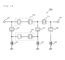
- FIG. 5A is a circuit diagram of a filter 50 using piezoelectric resonators, according to a second embodiment of the present invention.
- the filter 50 of the second embodiment includes three series piezoelectric resonators 11a to 11c; four parallel piezoelectric resonators 12a to 12d; four inductors 13a to 13d; and an additional piezoelectric resonator 14.
- the series piezoelectric resonators 11a to 11c are connected in series between an input terminal 15a and an output terminal 15b.
- First electrodes of the parallel piezoelectric resonators 12a to 12d are connected to connection points between the input terminal 15a and the series piezoelectric resonator 11a, between the series piezoelectric resonators 11a and 11b, between the series piezoelectric resonators 11b and 11c, and between the series piezoelectric resonator 11c and the output terminal 15b, respectively.
- Second electrodes of the parallel piezoelectric resonators 12a to 12d are connected to first terminals of the inductors 13a to 13d, respectively. Second terminals of the inductors 13a to 13d are grounded.
- the additional piezoelectric resonator 14 is connected between the second electrode of the parallel piezoelectric resonator 12b and the second electrode of the parallel piezoelectric resonator 12c. Note that the additional piezoelectric resonator 14 can be connected between any two second electrodes of the parallel piezoelectric resonators 12a to 12d. That is, the connection pattern is not limited to that shown in FIG. 5A and other connection patterns, such as those shown in FIGS. 5B to 5F, may be employed.
- the equivalent circuit of the series network shown in FIG. 2 can be added. Accordingly, by appropriately controlling the resonance frequency f 0 , the attenuation band can be provided at any desired location.
- an additional piezoelectric resonator is inserted between any two second electrodes of the parallel piezoelectric resonators.
- the second embodiment describes the case where a single additional piezoelectric resonator 14 is connected between any two second electrodes of the parallel piezoelectric resonators 12a to 12d
- two additional piezoelectric resonators 14 may be connected under conditions where, as shown in FIGS. 6A to 6C, the two additional piezoelectric resonators each are connected between any two second electrodes of the parallel piezoelectric resonators 12a to 12d such that the connection points are not connected with each other.
- the number of additional piezoelectric resonators is not limited to one or two, and can be freely chosen depending on the desired band-pass characteristics, product size/cost, or the like.
- the number of additional piezoelectric resonators to be connected to the parallel piezoelectric resonator is preferably one in terms of characteristics, as shown in circuits of FIGS. 5A to 5F, 6A to 6C, and 7A to 7X; however, a plurality of additional piezoelectric resonators may be connected to a single parallel piezoelectric resonator, as shown in circuits of FIGS. 8A and 8B. With this configuration too, by appropriately setting the material, thickness, size, etc. , of thepiezoelectricmaterial layer, desired band-pass characteristics can be sufficiently obtained.
- inductors 13a to 13d connected to the second electrodes of the parallel piezoelectric resonators 12a to 12d inductors which do not have the additional piezoelectric resonator 14 connected thereto can be eliminated.
- the second electrodes of the parallel piezoelectric resonators which do not have the additional piezoelectric resonator connected thereto may be directly grounded (see FIG. 9, for example).
- inductors may be inserted between an input terminal and a series piezoelectric resonator and between a series piezoelectric resonator and an output terminal (see FIG. 10, for example).
- the values of the inductors included in the filter of the present invention can be reduced with respect to conventional filters (see FIG. 25, for example) by inserting an additional piezoelectric resonator.
- the filter of the present invention is normally formed on a semiconductor substrate, the inductors necessary for the filter can be formed using parasitic inductors such as electrodes, wiring, bonding wires, and bumps.
- An exemplary semiconductor chip 110 in which the inductors are formed using wiring is shown in FIG. 11A, and an exemplary semiconductor package 111 in which the inductors are formed using bonding wires is shown in FIG. 11B.
- a semiconductor chip having formed thereon a filter may be arranged on a printed circuit board or a low temperature co-fired ceramic (LTCC) substrate as necessary.
- LTCC low temperature co-fired ceramic
- FIG. 11A is a top view of the semiconductor chip 110 which includes the circuit of the filter 50 shown in FIG. 5A.
- the gridded areas represent the upper electrodes of the piezoelectric resonators 11a to 11c, 12a to 12d, and 14, the dotted areas represent upper-layer wiring, and the diagonally lined areas represent lower-layer wiring or the inductors 13a to 13d.
- the second electrode of the parallel piezoelectric resonator 12b is formed in the "upper layer” and the second electrode of the parallel piezoelectric resonator 12c is formed in the "lower layer"
- the insertion of the additional piezoelectric resonator 14 can be more easily done.
- the second electrodes of the parallel piezoelectric resonators 12a and 12c are formed in the same layer and the second electrodes of the parallel piezoelectric resonators 12b and 12d are formed in the same layer.
- the third embodiment describes a filter configuration which enables the insertion of an additional piezoelectric resonator between the upper and lower layers by adjusting the number of piezoelectric resonators.
- FIGS. 13 and 14 are exemplary circuit diagrams of a filter using piezoelectric resonators, according to the third embodiment, which employs such a configuration.
- FIG. 13 is a diagram showing the configuration of a filter 130 using an additional piezoelectric resonator 134 having two piezoelectric resonators connected to each other in series.
- the additional piezoelectric resonator 134 can be inserted between the parallel piezoelectric resonators 12a and 12c.
- FIG. 14 is a diagram showing the configuration of a filter 140 in which a piezoelectric resonator 141 is further added on the series piezoelectric resonator side and the electrodes of an additional piezoelectric resonator 14 are made in different layers.
- the additional piezoelectric resonator can be configured in such a manner as that of a series piezoelectric resonator 151 or an additional piezoelectric resonator 154 shown in FIG. 15.
- FIG. 21 General structures of the series, parallel, and additional piezoelectric resonators to be used in the filter of each embodiment of the present invention are described in FIG. 21. In addition to this, another structure may be employed. A structure of a piezoelectric resonator other than that shown in FIG. 21 will be described below.
- the cavity 215 is covered with the insulating material layer 214, however, as shown in FIG. 16, a cavity 165 may be provided so as not to be fully covered with an insulating material layer 214.
- a substance being filled in the cavity 165 can be removed by etching.
- the cavity may be in any shape as long as the cavity does not hinder the vibration of the vibrating portion 218; for example, the opening of the cavity may be polygonal, circular, or elliptical shape, in addition to a quadrangular shape. Alternatively, the cavity may be tapered as viewed from the side surface. The cavity may be provided to penetrate through the lower part of the substrate 216.
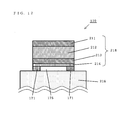
- a piezoelectric resonator 180 shown in FIGS. 18 and 19 is structured such that a vibrating portion 218 including an upper electrode layer 211, a lower electrode layer 213, and a piezoelectric material layer 212 sandwiched between the upper and lower electrode layers 211 and 213, is arranged on an acoustic multilayer film and the acoustic multilayer film is provided on a substrate 216.
- the acoustic multilayer film is formed by alternately stacking low acoustic impedance layers 184 and high acoustic impedance layers 185 each having a quarter-wavelength thickness.
- the first layer of the acoustic multilayer film as viewed from the vibrating portion 218 is made using a low impedance layer 184 so that the load impedance with respect to the piezoelectric material layer 212 becomes sufficiently low, whereby the piezoelectric material layer 212 and the substrate 216 are acoustically isolated.
- the vibrating portion 218 approaches free-vibration conditions where the vibrating portion 218 is not supported by anything, and operates in the same manner as that of the piezoelectric resonator 210 of FIG. 21.
- a material such as silicon dioxide (SiO 2 ) or silicon nitride (Si 3 N 4 ) may be used.
- a material such as aluminum nitride (AlN) , zinc oxide (ZnO), molybdenum (Mo), hafnium oxide (HfO 2 ), titanium oxide (TiO 2 ) or zirconium oxide (ZrO 2 ) may be used.
- the layer configuration of the piezoelectric resonator 210 is merely an example; even if a thin piezoelectric material layer is provided as a passivation film over the upper electrode, or even if an insulating layer is provided between the piezoelectric material layer and the electrode, the same advantage as that obtained by the piezoelectric resonator 210 can be obtained.
- the components of the present invention are not limited to those of the piezoelectric resonator 210.
- the upper electrode layer 211, the piezoelectric material layer 212, the lower electrode layer 213, and the insulating material layer 214 which make up the vibrating portion 218 may have different sizes in area.
- all layers of each piezoelectric resonator, except the upper electrode layer 211 and the lower electrode layer 213, may be formed integrally.
- the same advantage can be obtained.
- FIG. 20 is a diagram showing an exemplary surface acoustic wave filter 200 using surface acoustic wave resonators as the piezoelectric resonators of the filter 10 according to the foregoing first embodiment.
- a surface acoustic wave resonator is formed such that an interdigital transducer electrode and a reflector electrode are arranged on a piezoelectric substrate 206 so as to be close to each other with respect to the propagation direction.
- the surface acoustic wave filter 200 is configured such that series surface acoustic wave resonators 201a to 201c, parallel surface acoustic wave resonators 202a to 202d, and an additional surface acoustic wave resonator 204 are formed on the piezoelectric substrate 206 and these resonators are connected to one another by wired electrodes on the piezoelectric substrate 206.
- the resonance frequencies of the surface acoustic wave resonators are optimally set by adjusting an electrode finger pitch, a metalization ratio, the thickness of an electrode film, or the like, so as to obtain desired filter characteristics.
- a first electrode pad 205a is connected to one of the input and output terminals through an inductance component, and a second electrode pad 205b is connected to the other one of the input and output terminals through an inductance component.
- Ground electrode pads 203a to 203d are connected to the parallel surface acoustic wave resonators 202a to 202d and grounded through inductance components . Further, the additional surface acoustic wave resonator 204 is connected between ground electrode pads 203b and 203c.
Landscapes
- Physics & Mathematics (AREA)
- Acoustics & Sound (AREA)
- Chemical & Material Sciences (AREA)
- Crystallography & Structural Chemistry (AREA)
- Piezo-Electric Or Mechanical Vibrators, Or Delay Or Filter Circuits (AREA)
Applications Claiming Priority (2)
| Application Number | Priority Date | Filing Date | Title |
|---|---|---|---|
| JP2003391110 | 2003-11-20 | ||
| JP2003391110 | 2003-11-20 |
Publications (2)
| Publication Number | Publication Date |
|---|---|
| EP1533897A2 true EP1533897A2 (de) | 2005-05-25 |
| EP1533897A3 EP1533897A3 (de) | 2010-06-30 |
Family
ID=34431607
Family Applications (1)
| Application Number | Title | Priority Date | Filing Date |
|---|---|---|---|
| EP04026155A Withdrawn EP1533897A3 (de) | 2003-11-20 | 2004-11-04 | Filter mit piezoelektrischem Resonator |
Country Status (4)
| Country | Link |
|---|---|
| US (1) | US7138888B2 (de) |
| EP (1) | EP1533897A3 (de) |
| KR (1) | KR20050049362A (de) |
| CN (1) | CN1619958B (de) |
Cited By (1)
| Publication number | Priority date | Publication date | Assignee | Title |
|---|---|---|---|---|
| US12500566B2 (en) | 2022-07-26 | 2025-12-16 | Chengdu Boe Optoelectronics Technology Co., Ltd. | Filter, radio frequency device and electronic apparatus |
Families Citing this family (22)
| Publication number | Priority date | Publication date | Assignee | Title |
|---|---|---|---|---|
| KR100635268B1 (ko) * | 2004-05-17 | 2006-10-19 | 삼성전자주식회사 | 인덕터가 내장된 필터, 듀플렉서 및 그 제조방법 |
| US7554422B2 (en) * | 2004-09-10 | 2009-06-30 | Panasonic Corporation | Filter module using piezoelectric resonators, duplexer, communication device, and method for fabricating filter module |
| JP4446922B2 (ja) * | 2005-04-21 | 2010-04-07 | 富士通メディアデバイス株式会社 | フィルタおよび分波器 |
| US20070035364A1 (en) * | 2005-08-11 | 2007-02-15 | Uppili Sridhar | Titanium-tungsten alloy based mirrors and electrodes in bulk acoustic wave devices |
| EP1944867B1 (de) * | 2005-11-01 | 2011-08-24 | Murata Manufacturing Co., Ltd. | Elastikwellen-filtervorrichtung |
| KR101238358B1 (ko) * | 2006-02-06 | 2013-03-04 | 삼성전자주식회사 | 대역 통과 필터 및 이를 구비한 듀플렉서 |
| KR101238359B1 (ko) * | 2006-02-06 | 2013-03-04 | 삼성전자주식회사 | 듀플렉서 |
| JP5072974B2 (ja) * | 2007-11-15 | 2012-11-14 | 太陽誘電株式会社 | 弾性波デバイス、それを用いたデュープレクサおよびそのデュープレクサを用いた通信機 |
| US8902020B2 (en) * | 2009-07-27 | 2014-12-02 | Avago Technologies General Ip (Singapore) Pte. Ltd. | Resonator filter with multiple cross-couplings |
| EP2680285A4 (de) | 2011-02-25 | 2017-09-13 | Murata Manufacturing Co., Ltd. | Element mit variabler kapazität und abstimmbarer filter |
| CN102291095A (zh) * | 2011-04-27 | 2011-12-21 | 庞慰 | 复合体声波谐振器 |
| JP5907254B2 (ja) | 2012-04-10 | 2016-04-26 | 株式会社村田製作所 | ラダー型弾性表面波フィルタ |
| CN103532514A (zh) * | 2012-07-03 | 2014-01-22 | 四川蓝讯宝迩电子科技有限公司 | 基于滤波器的滤波电路 |
| CN104508978A (zh) * | 2012-08-30 | 2015-04-08 | 株式会社村田制作所 | 滤波器装置以及双工器 |
| CN104716926A (zh) * | 2013-12-17 | 2015-06-17 | 贵州中科汉天下电子有限公司 | 压电滤波器 |
| JP6662150B2 (ja) * | 2016-03-31 | 2020-03-11 | 株式会社村田製作所 | ハイパスフィルタ |
| CN109643984B (zh) * | 2016-06-21 | 2023-09-01 | 诺思(天津)微系统有限责任公司 | 一种梯形结构宽带压电滤波器 |
| CN106656098B (zh) * | 2016-12-23 | 2020-11-24 | 无锡市好达电子有限公司 | 一种超大带宽声表面波滤波器 |
| JP6854891B2 (ja) | 2017-07-04 | 2021-04-07 | 京セラ株式会社 | 弾性波装置、分波器および通信装置 |
| CN110995197B (zh) * | 2019-12-02 | 2024-06-11 | 武汉衍熙微器件有限公司 | 一种可调节抑制的声波滤波器装置 |
| WO2021149332A1 (ja) * | 2020-01-24 | 2021-07-29 | 株式会社村田製作所 | フィルタ装置、マルチプレクサ、高周波フロントエンド回路及び通信装置 |
| CN114337594B (zh) * | 2021-12-24 | 2025-12-30 | 北京中科汉天下电子技术有限公司 | 滤波电路和双工器 |
Family Cites Families (21)
| Publication number | Priority date | Publication date | Assignee | Title |
|---|---|---|---|---|
| JP2800905B2 (ja) | 1991-10-28 | 1998-09-21 | 富士通株式会社 | 弾性表面波フィルタ |
| US6137380A (en) * | 1996-08-14 | 2000-10-24 | Murata Manufacturing, Co., Ltd | Surface acoustic wave filter utilizing a particularly placed spurious component of a parallel resonator |
| JPH10200370A (ja) * | 1997-01-10 | 1998-07-31 | Murata Mfg Co Ltd | 弾性表面波フィルタ |
| DE69722168T2 (de) * | 1997-02-12 | 2003-12-18 | Oki Electric Ind Co Ltd | Akustische Oberflächenwellenfilter mit erzeugten Dämpfungspolen durch Impedanzschaltungen |
| JP3161439B2 (ja) * | 1998-11-25 | 2001-04-25 | 株式会社村田製作所 | 弾性表面波フィルタ |
| JP3498204B2 (ja) * | 1999-03-10 | 2004-02-16 | 株式会社村田製作所 | 弾性表面波フィルタ、それを用いた通信機装置 |
| US6262637B1 (en) * | 1999-06-02 | 2001-07-17 | Agilent Technologies, Inc. | Duplexer incorporating thin-film bulk acoustic resonators (FBARs) |
| DE19932649A1 (de) * | 1999-07-13 | 2001-02-08 | Epcos Ag | SAW-Filter des Reaktanzfiltertyps mit verbesserter Sperrbereichsunterdrückung und Verfahren zur Optimierung der Sperrbereichsunterdrückung |
| JP3387469B2 (ja) * | 2000-01-18 | 2003-03-17 | 株式会社村田製作所 | 弾性表面波装置及び弾性表面波フィルタ |
| JP2002141771A (ja) * | 2000-08-21 | 2002-05-17 | Murata Mfg Co Ltd | 弾性表面波フィルタ装置 |
| JP3614369B2 (ja) * | 2001-01-11 | 2005-01-26 | 沖電気工業株式会社 | 有極型sawフィルタ |
| JP2002314372A (ja) * | 2001-02-07 | 2002-10-25 | Murata Mfg Co Ltd | 弾性表面波フィルタ装置 |
| JP3973915B2 (ja) * | 2001-03-30 | 2007-09-12 | 株式会社日立メディアエレクトロニクス | 高周波フィルタ、高周波回路、アンテナ共用器及び無線端末 |
| DE10296803B4 (de) * | 2001-05-11 | 2008-04-10 | Ube Industries, Ltd., Ube | Duplexer mit FBAR-Abgleichresonator |
| JP3948550B2 (ja) * | 2001-09-25 | 2007-07-25 | Tdk株式会社 | 弾性表面波装置 |
| JP4154949B2 (ja) * | 2002-08-06 | 2008-09-24 | 松下電器産業株式会社 | Sawフィルタ |
| JP2004173245A (ja) * | 2002-10-30 | 2004-06-17 | Murata Mfg Co Ltd | ラダー型フィルタ、分波器、および通信機 |
| JP3815424B2 (ja) * | 2002-11-08 | 2006-08-30 | 株式会社村田製作所 | 弾性境界波装置 |
| DE10258422A1 (de) * | 2002-12-13 | 2004-06-24 | Epcos Ag | Mit akustischen Volumenwellen arbeitendes Bauelement mit gekoppelten Resonatoren |
| KR20050035904A (ko) * | 2003-10-07 | 2005-04-20 | 삼성전기주식회사 | 공통접지 인덕터를 구비한 래더형 벌크탄성파 필터 |
| DE60316457T2 (de) * | 2003-12-22 | 2008-06-19 | Infineon Technologies Ag | Dünnfilmresonator-Abzweigfilter und Verfahren zur Erdung dieser Filter |
-
2004
- 2004-11-04 EP EP04026155A patent/EP1533897A3/de not_active Withdrawn
- 2004-11-10 US US10/984,839 patent/US7138888B2/en not_active Expired - Fee Related
- 2004-11-17 KR KR1020040093939A patent/KR20050049362A/ko not_active Withdrawn
- 2004-11-19 CN CN2004100956717A patent/CN1619958B/zh not_active Expired - Fee Related
Cited By (1)
| Publication number | Priority date | Publication date | Assignee | Title |
|---|---|---|---|---|
| US12500566B2 (en) | 2022-07-26 | 2025-12-16 | Chengdu Boe Optoelectronics Technology Co., Ltd. | Filter, radio frequency device and electronic apparatus |
Also Published As
| Publication number | Publication date |
|---|---|
| EP1533897A3 (de) | 2010-06-30 |
| CN1619958B (zh) | 2011-05-11 |
| CN1619958A (zh) | 2005-05-25 |
| KR20050049362A (ko) | 2005-05-25 |
| US20050110596A1 (en) | 2005-05-26 |
| US7138888B2 (en) | 2006-11-21 |
Similar Documents
| Publication | Publication Date | Title |
|---|---|---|
| EP1533897A2 (de) | Filter mit piezoelektrischem Resonator | |
| JP5296282B2 (ja) | バルク音響波装置 | |
| US6885260B2 (en) | Filter using film bulk acoustic resonator and transmission/reception switch | |
| CN112673569B (zh) | 双级横向体声波滤波器 | |
| JP4068218B2 (ja) | 結晶フィルター構造および薄膜バルク弾性波共振器を利用したフィルター | |
| US7616079B2 (en) | Bulk acoustic wave resonator and circuit comprising same | |
| KR100809120B1 (ko) | 사다리형 필터, 무선 주파수 대역 통과 필터, 무선 주파수수신기 및/또는 송신기 장치 | |
| US7301420B2 (en) | Piezoelectric resonator filter | |
| US7479847B2 (en) | Filter using piezoelectric resonator | |
| KR20040066036A (ko) | 래더형 필터, 분파기, 및 통신 장치 | |
| EP1478091A2 (de) | Filtereinrichtung mit scharfer Dämpfung in schmaler Bandbreite und Abzweigfilter mit einer solchen Filtereinrichtung | |
| JPH10341135A (ja) | 弾性表面波装置 | |
| JP3244032B2 (ja) | 弾性表面波装置 | |
| CN119834757A (zh) | Rf滤波器装置 | |
| JP2008532334A (ja) | 圧電フィルタならびにそれを用いた共用器および通信機器 | |
| US7515017B2 (en) | Surface acoustic wave device utilizing a terminal routing pattern | |
| WO2019078157A1 (ja) | 弾性波フィルタ、マルチプレクサ、高周波フロントエンド回路および通信装置 | |
| US7242130B2 (en) | Piezoelectric device, antenna duplexer, and method of manufacturing piezoelectric resonators used therefor | |
| JP2003179518A (ja) | 薄膜圧電共振器を用いたフィルタ及び送受切換器 | |
| JP4390682B2 (ja) | 圧電共振器を用いたフィルタ | |
| WO2018139320A1 (ja) | 高周波フィルタ、高周波フロントエンド回路及び通信装置 | |
| JP3859573B2 (ja) | 弾性表面波フィルタ及びフィルタ装置 | |
| CN101128977A (zh) | 压电滤波器以及使用该压电滤波器的双工器和通信装置 | |
| WO2004066494A1 (en) | Resonator filter structure with improved balance | |
| US11923827B2 (en) | Bulk acoustic wave resonator stacked onto an integrated passive device |
Legal Events
| Date | Code | Title | Description |
|---|---|---|---|
| PUAI | Public reference made under article 153(3) epc to a published international application that has entered the european phase |
Free format text: ORIGINAL CODE: 0009012 |
|
| AK | Designated contracting states |
Kind code of ref document: A2 Designated state(s): AT BE BG CH CY CZ DE DK EE ES FI FR GB GR HU IE IS IT LI LU MC NL PL PT RO SE SI SK TR |
|
| AX | Request for extension of the european patent |
Extension state: AL HR LT LV MK YU |
|
| RAP1 | Party data changed (applicant data changed or rights of an application transferred) |
Owner name: PANASONIC CORPORATION |
|
| PUAL | Search report despatched |
Free format text: ORIGINAL CODE: 0009013 |
|
| AK | Designated contracting states |
Kind code of ref document: A3 Designated state(s): AT BE BG CH CY CZ DE DK EE ES FI FR GB GR HU IE IS IT LI LU MC NL PL PT RO SE SI SK TR |
|
| AX | Request for extension of the european patent |
Extension state: AL HR LT LV MK YU |
|
| 17P | Request for examination filed |
Effective date: 20100806 |
|
| 17Q | First examination report despatched |
Effective date: 20100827 |
|
| AKX | Designation fees paid |
Designated state(s): AT BE BG CH CY CZ DE DK EE ES FI FR GB GR HU IE IS IT LI LU MC NL PL PT RO SE SI SK TR |
|
| STAA | Information on the status of an ep patent application or granted ep patent |
Free format text: STATUS: THE APPLICATION IS DEEMED TO BE WITHDRAWN |
|
| 18D | Application deemed to be withdrawn |
Effective date: 20130724 |