EP1478091A2 - Filtereinrichtung mit scharfer Dämpfung in schmaler Bandbreite und Abzweigfilter mit einer solchen Filtereinrichtung - Google Patents
Filtereinrichtung mit scharfer Dämpfung in schmaler Bandbreite und Abzweigfilter mit einer solchen Filtereinrichtung Download PDFInfo
- Publication number
- EP1478091A2 EP1478091A2 EP04011415A EP04011415A EP1478091A2 EP 1478091 A2 EP1478091 A2 EP 1478091A2 EP 04011415 A EP04011415 A EP 04011415A EP 04011415 A EP04011415 A EP 04011415A EP 1478091 A2 EP1478091 A2 EP 1478091A2
- Authority
- EP
- European Patent Office
- Prior art keywords
- resonator
- resonators
- filter device
- those
- different
- Prior art date
- Legal status (The legal status is an assumption and is not a legal conclusion. Google has not performed a legal analysis and makes no representation as to the accuracy of the status listed.)
- Granted
Links
- 230000008878 coupling Effects 0.000 claims abstract description 77
- 238000010168 coupling process Methods 0.000 claims abstract description 77
- 238000005859 coupling reaction Methods 0.000 claims abstract description 77
- 239000000758 substrate Substances 0.000 claims abstract description 21
- 238000010897 surface acoustic wave method Methods 0.000 claims description 26
- 239000010408 film Substances 0.000 description 38
- VYPSYNLAJGMNEJ-UHFFFAOYSA-N Silicium dioxide Chemical compound O=[Si]=O VYPSYNLAJGMNEJ-UHFFFAOYSA-N 0.000 description 12
- 238000003780 insertion Methods 0.000 description 7
- 230000037431 insertion Effects 0.000 description 7
- 229910052681 coesite Inorganic materials 0.000 description 6
- 229910052906 cristobalite Inorganic materials 0.000 description 6
- 239000000377 silicon dioxide Substances 0.000 description 6
- 229910052682 stishovite Inorganic materials 0.000 description 6
- 229910052905 tridymite Inorganic materials 0.000 description 6
- 238000010586 diagram Methods 0.000 description 5
- 230000005540 biological transmission Effects 0.000 description 4
- 230000007613 environmental effect Effects 0.000 description 4
- 238000000034 method Methods 0.000 description 4
- 238000010295 mobile communication Methods 0.000 description 4
- 239000010409 thin film Substances 0.000 description 4
- 230000017105 transposition Effects 0.000 description 4
- 238000004891 communication Methods 0.000 description 3
- 239000013078 crystal Substances 0.000 description 3
- 230000005684 electric field Effects 0.000 description 3
- 239000000463 material Substances 0.000 description 3
- 239000000919 ceramic Substances 0.000 description 2
- 230000000694 effects Effects 0.000 description 2
- 239000011521 glass Substances 0.000 description 2
- 229910052710 silicon Inorganic materials 0.000 description 2
- 239000010703 silicon Substances 0.000 description 2
- 229910012463 LiTaO3 Inorganic materials 0.000 description 1
- 239000000654 additive Substances 0.000 description 1
- 230000000996 additive effect Effects 0.000 description 1
- 238000007796 conventional method Methods 0.000 description 1
- 238000005530 etching Methods 0.000 description 1
- HFGPZNIAWCZYJU-UHFFFAOYSA-N lead zirconate titanate Chemical compound [O-2].[O-2].[O-2].[O-2].[O-2].[Ti+4].[Zr+4].[Pb+2] HFGPZNIAWCZYJU-UHFFFAOYSA-N 0.000 description 1
- 238000004519 manufacturing process Methods 0.000 description 1
- 230000001902 propagating effect Effects 0.000 description 1
Images


Classifications
-
- H—ELECTRICITY
- H03—ELECTRONIC CIRCUITRY
- H03H—IMPEDANCE NETWORKS, e.g. RESONANT CIRCUITS; RESONATORS
- H03H9/00—Networks comprising electromechanical or electro-acoustic elements; Electromechanical resonators
- H03H9/46—Filters
- H03H9/64—Filters using surface acoustic waves
- H03H9/6423—Means for obtaining a particular transfer characteristic
- H03H9/6426—Combinations of the characteristics of different transducers
-
- H—ELECTRICITY
- H03—ELECTRONIC CIRCUITRY
- H03H—IMPEDANCE NETWORKS, e.g. RESONANT CIRCUITS; RESONATORS
- H03H9/00—Networks comprising electromechanical or electro-acoustic elements; Electromechanical resonators
- H03H9/46—Filters
- H03H9/54—Filters comprising resonators of piezoelectric or electrostrictive material
- H03H9/58—Multiple crystal filters
- H03H9/60—Electric coupling means therefor
- H03H9/605—Electric coupling means therefor consisting of a ladder configuration
Definitions
- the present invention relates to a filter device and a branching filter using the filter device, in particular to a technique effectively applicable to an improvement of sharpness of filter characteristic between pass band and prohibition band in the filter device.
- the mobile communication terminal equipment such as a portable telephone and the like has been rapidly developed. Subsequently, it is desired that the mobile communication terminal equipment is small in size, light in weight and capable of saving electric power for the purpose of convenience for portability thereof.
- the filter device used therein is not only small in size and light in weight but also low in insertion loss. Further, from the view point of high speed and large capacity communication, it is also required that the filter device has a wide pass band characteristic.
- ladder type filters In order to meet the requirement, many filter devices each of which a plurality of resonators are connected to each other like a comb, namely ladder type filters are used as a filter device of the mobile communication terminal equipment.
- SAW surface acoustic wave
- BAW bulk acoustic wave
- the ladder type filter may be constituted by thin film resonators each using a thin film of piezo-electricity.
- Japanese unexamined patent publication Hei 10-93375 namely No.93375/1998 discloses a technique that an inductance element is added in a parallel arm or that frequency differences are made between resonance frequencies of resonators formed in a serial arm and anti-resonance frequencies of resonators formed in a parallel arm.
- the filter device has not only pressure temperature dependence that temperature of the filter device varies characteristics thereof but also individual difference due to unevenness of manufacturing the filter device. It is therefore necessary not only that pass-band width capable of obtaining the insertion loss fulfilling the above specification is enlarged but also that cut-off band width capable of obtaining the amount of attenuation fulfilling the described specification is enlarged. As a result, the pass-band and the cut-off band become close to each other.
- a filter device which is constituted by circuit elements formed on a single substrate, said circuit elements comprising: a first wiring section which is formed between an input signal electrode and an output signal electrode; at least one first resonator which is located in said first wiring section and which has a predetermined resonance frequency; at least one second wiring section which is formed between said first wiring section and a ground electrode; a second resonator which is located in said second wiring section and which has an anti-resonance frequency forming a pass-band with said predetermined resonance frequency of said at least one first resonator; and an effective electric and mechanical coupling factor of at least any one of said first and second resonators being different from those of the other resonators.
- the filter device becomes capable of obtaining attenuation characteristic of sharpness in a narrow band width by making the effective electric and mechanical coupling factor of at least any one of the first and the second resonators be different from those of the other resonators.
- said resonator of which the effective electric and mechanical coupling factor is different from those of the other resonators may be determined to be between a frequency in the pass-band side edge in the attenuation band of the filter device and a frequency in the attenuation band side edge in the pass-band of the filter device.
- a plurality of said second resonators may be located in said second wiring sections, the effective electric and mechanical coupling factor of a part of said second resonators may be different from those of the other said second resonators and said first resonator.
- said second resonator has a value of the effective electric and mechanical coupling factor different from those of the first resonator while the other said second resonator has the same value thereof as those of the first resonator, an impedance of said second resonator may be made lower than those of the other said second resonator.
- a plurality of said first resonators may be located in said first wiring sections, the effective electric and mechanical coupling factor of a part of said first resonators may be different from those of the other said first resonators and said second resonator.
- said first resonator has a value of the effective electric and mechanical coupling factor different from those of the second resonator while the other said first resonator has the same value thereof as those of the second resonator, an impedance of said first resonator may be made lower than those of the other said first resonator.
- anti-resonance frequency of said second resonator may be made higher than resonance frequency of said first resonator having the same value of the effective electric and mechanical coupling factor as those of said second resonator.
- the effective electric and mechanical coupling factor of said first resonator is different from that of said second resonator.
- said first resonator and said second resonator may be SAW resonators each using surface acoustic wave (SAW).
- SAW surface acoustic wave
- said first resonator and said second resonator may be piezo-electric resonators each using bulk acoustic wave (BAW).
- BAW bulk acoustic wave
- said piezo-electric resonators may be diaphragm-type piezo-electric resonators or SMR (Solidly Mounted Resonator)-type piezo-electric resonators.
- the effective electric and mechanical coupling factor of said resonator is different from those of the other resonators by a capacitance element connected in serial or in parallel to the resonator.
- the effective electric and mechanical coupling factor of said resonator may be different from those of the other resonators by making normalized film thickness or duty of said resonator be different from those of the other resonators.
- the effective electric and mechanical coupling factor of said resonator may be different from those of the other resonators by making film thickness of an oxide film formed on a surface of a piezo-electric film constituting said resonator be different from those of the other resonators.
- the effective electric and mechanical coupling factor of said resonator may be different from those of the other resonators by making an area of an electrode constituting said resonator be different from those of the other resonators.
- the effective electric and mechanical coupling factor of said resonator may be different from those of the other resonators by making film thickness of an electrode constituting said resonator be different from those of the other resonators.
- a branching filter comprising a plurality of filter devices each of which is constituted by circuit elements formed on a single substrate, said circuit elements including: a first wiring section which is formed between an input signal electrode and an output signal electrode; at least one first resonator which is located in said first wiring section and which has a predetermined resonance frequency; at least one second wiring section which is formed between said first wiring section and a ground electrode; a second resonator which is located in said second wiring section and which has an anti-resonance frequency forming a pass-band with said predetermined resonance frequency of said at least one first resonator; and an effective electric and mechanical coupling factor of at least any one of said first and second resonators being different from those of the other resonators.
- the branching filter becomes capable of obtaining attenuation characteristic of sharpness in a narrow band width.
- the conventional ladder type filter comprises a first wiring section 103, three resonators 104a, 104b, 104c, second wiring sections 106a, 106b, 106c, 106d, and four resonators 107a, 107b, 107c and 107d.
- the first wiring section 103 is formed between an input signal electrode 101 and an output signal electrode 102 as a serial arm.
- the three resonators 104a, 104b, 104c are connected in serial to the first wiring section 103.
- the second wiring sections 106a, 106b, 106c, 106d are formed as parallel arms.
- the second wiring section 106a is formed between a ground electrode 105 and an intermediate point of the input signal electrode 101 and the resonator 104a.
- the second wiring section 106b is formed between the ground electrode 105 and an intermediate point of the resonator 104a and the resonator 104b.
- the second wiring section 106c is formed between, the ground electrode 105 and an intermediate point of the resonator 104b and the resonator 104c.
- the second wiring section 106d is formed between the ground electrode 105 and an intermediate point of the output signal electrode 102 and the resonator 104c.
- the four resonators 107a, 107b, 107c, 107d are connected in parallel through the second wiring sections 106a, 106b, 106c, 106d, respectively.
- Japanese unexamined patent publication Hei 10-93375 namely No.93375/1998 discloses a technique that an inductance element is added in a parallel arm or that frequency differences are made between resonance frequencies of resonators formed in a serial arm and anti-resonance frequencies of resonators formed in a parallel arm.
- Fig. 2 illustrated are respective impedance characteristics of the resonator S formed in the serial arm and the resonator P formed in the parallel arm both used in the conventional ladder type filter thus illustrated.
- impedances and frequencies are fairly changed in each of resonators formed in a serial arm and a parallel arm so that required insertion loss and attenuating amount may be achieved.
- illustrated are only the respective impedance characteristics of one resonator S formed in the serial arm and one resonator P formed in the parallel arm.
- Fig. 3 illustrated is an example of the pass-band characteristic of a ladder type filter using such resonators.
- an inductor component of a path connected to a ground plane is adequately adjusted in order that the attenuation may be obtained at a desired frequency band.
- a difference ds be considered in Fig. 3 so as to estimate an attenuation characteristic of the ladder type filter.
- the ds is defined as a difference between a frequency at which the attenuation is -4dB and a frequency at which the attenuation is -35dB.
- the attenuation characteristic becomes sharper, the difference ds becomes smaller.
- the difference ds at a lower frequency side of the pass-band was determined in the conventional ladder type filter illustrated in Fig. 3, so that the difference ds was 18.2 MHz.
- an insertion loss at a pass-band frequency fulfills a predetermined specification.
- a large amount of attenuation fulfilling a predetermined specification is obtained at a cut-off frequency (a pass-band frequency at the side of a communication partner in a transmission/reception filter device).
- a transmission filter fulfills an insertion loss of 3.8 dB at a pass-band frequency.
- the transmission filter obtains an amount of attenuation of -37 dB at a frequency band (cut-off frequency band) of 20 MHz higher than the pass-band frequency. In other words, a difference of 33.2 dB between higher and lower frequencies must be"made within a frequency band of 20 MHz.
- Fig. 4 is an equal circuit diagram for schematically showing a constitution of the filter device according to the first embodiment of the present invention.
- Fig. 5 is an explanation view for schematically showing a constitution of an SAW resonator as an example of a resonator used in the filter device illustrated in Fig. 4.
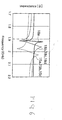
- Fig. 6 is a graph for showing an example of impedance characteristics of the resonators in the filter device illustrated in Fig. 4.
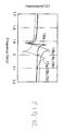
- Fig. 7 is a graph for showing a pass-band characteristic of the filter device having the impedance characteristics illustrated in Fig. 6.
- Fig. 8 is a sectional view for schematically showing a structure of a piezo-electric resonator as another example of a resonator used in the filter device illustrated in Fig. 4.
- Fig. 5 is an explanation view for schematically showing a constitution of an SAW resonator as an example of a resonator used in the filter device illustrated in Fig. 4.
- Fig. 6 is a graph for
- FIG. 9 is a sectional view for schematically showing a structure of a piezo-electric resonator as yet another example of a resonator used in the filter device illustrated in Fig. 4.
- Fig. 10 is a sectional view for schematically showing the SAW resonator taken from A-A line in Fig. 5.
- Fig. 11 is a graph for showing a relation between an area of an electrode and electric and mechanical coupling factor in a piezo-electric resonator.
- Fig. 12 is a graph for showing another example of impedance characteristics of the resonators in the filter device illustrated in Fig. 4.
- Fig. 13 is a graph for showing a pass-band characteristic of the filter device having the impedance characteristics illustrated in Fig. 12.
- the filter device 10 comprises predetermined circuit elements formed on a single substrate 11.
- the filter device 10 comprises a first wiring section (serial arm) 14, three resonators (first resonators) 15a, 15b, 15c, second wiring sections (parallel arms) 17a, 17b, 17c, 17d, and four resonators (second resonators) 18a, 18b, 18c and 18d, as the circuit elements.
- the first wiring section 14 ' is formed between an input signal electrode 12 and an output signal electrode 13 as a serial arm.
- the three resonators 15a, 15b, 15c are connected in serial to the first wiring section 14.
- the second wiring sections 17a, 17b, 17c, 17d are formed as parallel arms.
- the second wiring section 17a is formed between a ground electrode 16 and an intermediate point of the input signal electrode 12 and the resonator 15a.
- the second wiring section 17b is formed between the ground electrode 16 and an intermediate point of the resonator 15a and the resonator 15b.
- the second wiring section 17c is formed between the ground electrode 16 and an intermediate point of the resonator 15b and the resonator 15c.
- the second wiring section 17d is formed between the ground electrode 16 and an intermediate point of the output signal electrode 13 and the resonator 15c.
- the four resonators 18a, 18b, 18c, 18d are connected in parallel through the second wiring sections 17a, 17b, 17c, 17d, respectively.
- resonance frequencies of the resonators 15a, 15b, 15c of the first wiring section 14 as the serial arm are substantially corresponding with anti-resonance frequencies of the resonators 18a, 18b, 18c, 18d of the second wiring sections 17a, 17b, 17c, 17d as the parallel arms.
- a pass band is thereby formed so that a signal within a predetermined band width inputted to the input signal electrode 12 may be outputted from the output signal electrode 13.
- the number of the first resonators 15a, 15b, 15c as the serial arm resonators is not restricted to three while the number of the second resonators 18a, 18b, 18c, 18d as the parallel arm resonators is not restricted to four.
- one or a plurality of the first resonators 15a, 15b, 15c may be formed while one or a plurality of the second resonators 18a, 18b, 18c, 18d may be formed.
- the single substrate 11 is formed by a piezo-electric single crystal, such as LiNbOs, LiTaO 3 , crystal and the like, or formed by piezo-electric ceramics, such as lead titanate zirconate piezo-electric ceramics.
- a piezo-electric single crystal such as LiNbOs, LiTaO 3 , crystal and the like
- piezo-electric ceramics such as lead titanate zirconate piezo-electric ceramics.
- an insulating substrate. on which a piezo-electric thin film, such as a ZnO thin film and the like is formed may be used as the single substrate 11.
- each of the first resonators 15a, 15b, 15c and the second resonators 18a, 18b, 18c, 18d is constituted, for example, by an SAW resonator as illustrated in Fig. 5.
- the SAW resonator has a pair of electrode fingers each of which has a shape of the teeth of a comb with being involved in each other, namely, transposition finger-shaped electrodes 19a, 19b.
- a surface acoustic wave SAW
- SAW surface acoustic wave
- reflectors 20 reflecting the surface acoustic wave (SAW) are located at both sides of the SAW resonator.
- a capacitance element 21 is located in the second wiring section 17a as the parallel arm with the capacitance element 21 being connected in parallel with the second resonator 18a.
- an effective electric and mechanical coupling factor keff 2 of the second resonator 18a is different from those of the first resonators 15a, 15b, 15c and the other second resonators 18b, 18c, 18d. It is enough in this embodiment that the effective electric and mechanical coupling factor keff 2 of a part of the second resonators 18a, 18b, 18c, 18d formed in the second wiring sections 17a, 17b, 17c, 17d as the parallel arms is different from those of the other resonators.
- each effective electric and mechanical coupling factor keff 2 of a part of the second resonators 18b, 18c, 18d formed in the second wiring sections 17b, 17c, 17d as the parallel arms may be different from those of the other resonators.
- the capacitance element may be connected in serial with the second resonator.
- the effective electric and mechanical coupling factor keff 2 is defined by the following quotation in an impedance characteristic of a resonator, using a frequency fa of the maximum impedance and another frequency fr of the minimum impedance.
- keff 2 (fa 2 -fr 2 )/fr 2 ⁇ 100(%)
- the effective electric and mechanical coupling factors keff 2 of the first resonators 15a, 15b, 15c and the other second resonators 18b, 18c, 18d are determined to be 5.1(%).
- the effective electric and mechanical coupling factor keff 2 of the second resonator 18a is determined to be 0.95(%).
- a value of the effective electric and mechanical coupling factor keff 2 is not restricted to those shown in this embodiment. The value of the effective electric and mechanical coupling factor keff 2 can be freely determined.
- Fig. 6 illustrated are impedance characteristics of the first resonators 15a, 15b, 15c of the serial arm 14 and the second resonators 18a, 18b, 18c, 18d of the respective parallel arms 17a, 17b, 17c, 17d in the filter device 10 having the constitution thus mentioned.
- impedances and frequencies are fairly changed in each of resonators formed in a serial arm and a parallel arm so that required insertion loss and attenuating amount may be achieved.
- Fig. 7 illustrated is a pass-band characteristic of the filter device 10 according to this embodiment using such the resonators 15a, 15b, 15c, 18a, 18b, 18c, 18d.
- Fig. 7 so as to estimate an attenuation characteristic of the filter device 10.
- the difference ds between a frequency at which the attenuation is -4dB and a frequency at which the attenuation is -35dB be considered in Fig. 7.
- the difference ds in the lower frequency side of the pass-band is 14.8 MHz.
- the difference ds in the lower frequency side of the pass-band of the above-described conventional ladder type filter illustrated in Fig. 3 was 18.2 MHz, it can be understood that sharpness of attenuation characteristic is improved by 3.8 MHz.
- the effective electric and mechanical coupling factor keff 2 of the resonator 18a formed in the parallel arm 17a is different from those of the other resonators 15a, 15b, 15c, 18b, 18c, and 18d.
- the filter device 10 thereby becomes capable of obtaining attenuation characteristic of sharpness in a narrow band width. Accordingly, when characteristics of the filter device 10 are varied due to environmental temperature for using the filter device 10 and individual differences of the products thereof, desirable characteristics thereof can be stably obtained.
- Attenuation characteristic of sharpness can be obtained at a frequency side lower than the pass-band by making the effective electric and mechanical coupling factor keff 2 of the resonator 18a formed in the parallel arm 17a be different from those of the other resonators 15a, 15b, 15c, 18b, 18c, and 18d.
- a preferable range within which the effective electric and mechanical coupling factor keff 2 of a parallel arm resonator is different from that of the other resonator may be, for example, between 1/10 and 7/10 of that of a serial arm resonator.
- the effective electric and mechanical coupling factor keff 2 of the parallel arm resonator should be determined to be between 1/10 and 7/10 of an additive mean value of the effective electric and mechanical coupling factors keff 2 of the serial arm resonators.
- a resonance frequency of the parallel arm resonator (the resonator 18a in this embodiment) of which the effective electric and mechanical coupling factor keff 2 is different from those of the other resonators may be determined to be between a frequency in the pass-band side edge in the attenuation band of the filter device 10 and a frequency in the attenuation band side edge in the pass-band of the filter device 10.
- the resonance frequency of the parallel arm resonator (the resonator 18a in this embodiment) of which the effective electric and mechanical coupling factor keff 2 is different from those of the other resonators may be determined to be each resonance frequency of the other parallel arm resonators.
- an impedance of the parallel arm resonator (the resonator 18a in this embodiment) of which the effective electric and mechanical coupling factor keff 2 is different from those of the other resonators may also be determined in correspondence with required characteristics therefor.
- the impedance of the parallel arm resonator 18a is determined to be larger than each impedance of the other parallel arm resonators 18b, 18c, and 18d in this embodiment.
- piezo-electric resonators each using bulk acoustic wave (BAW) can be applied to the resonators in the present invention including this embodiment as well as the other embodiments which will be hereunder described.
- BAW bulk acoustic wave
- Figs. 8 and 9 illustrated are constitutions of the piezo-electric resonators that can be applied to the resonators in the present invention.
- the piezo-electric resonator illustrated in Fig. 8 is such one that is called “diaphragm-type piezo-electric resonator".
- the piezo-electric resonator comprises a substrate 11 consisting mainly of silicon or glass, protection layers 22, a piezo-electric film 23, a lower electrode 24, and an upper electrode 25.
- the protection layers 22 are made, for example of SiO 2 film (oxide film) or the like, and formed on both surfaces of the substrate 11.
- the lower electrode 24 and the upper electrode 25 are stacked with the piezo-electric film 23 consisting of AlN, ZnO or the like being interposed therebetween.
- the substrate 11 is partially cut out by an etching method and the like so that the bulk acoustic wave (BAW) may be readily propagating through the substrate 11.
- BAW bulk acoustic wave
- the piezo-electric resonator illustrated in Fig. 9 is such one that is called "SMR (Solidly Mounted Resonator)-type piezo-electric resonator".
- the piezo-electric resonator comprises a substrate 11, a reflection film member 26, a lower electrode 24, a piezo-electric film 23, a dielectric film 27, and an upper electrode 25.
- the substrate 11 is consisting mainly of silicon or glass.
- the reflection film member 26 is stacked on a principal surface of the substrate 11.
- the reflection film member 26 is consisting of materials of high acoustic impedance, for example, SiO 2 films 26a and another materials of low acoustic impedance, for example, AlN films 26b with both the materials being stacked alternately on each other.
- the lower electrode 24 and the upper electrode 25 are stacked with the piezo-electric film 23 consisting of AlN, ZnO or the like being interposed therebetween.
- the dielectric film 27 is consisting, for example of SiO 2 film (oxide film) or the like and formed between the piezo-electric film 23 and the upper electrode 25.
- SAW resonators or piezo-electric resonators can be applied to the resonators.
- means for making the effective electric and mechanical coupling factor keff 2 of a part of the resonators be different from those of the other resonators the following means can be considered in addition to the above-described means, namely, using the capacitance element.
- the effective electric and mechanical coupling factor keff 2 of a part of resonators can be different from those of the other resonators by making normalized film thickness h/ ⁇ of the part of resonators be different from those of the other resonators.
- the effective electric and mechanical coupling factor keff 2 of a part of resonators can be different from those of the other resonators by making duty L2/L1 of the part of resonators be different from those of the other resonators.
- the effective electric and mechanical coupling factor keff 2 of a part of the resonators can be different from those of the other resonators by making a film thickness of the SiO 2 film formed on a surface of the piezo-electric film 23 (the SiO 2 film is the protection layer 22 at the side of the lower electrode 24 in a case shown in Fig. 8 while the SiO 2 film is the dielectric film 27 in a case shown in Fig. 9) of the part of the resonators be different from those of the other resonators.
- a film thickness of the SiO 2 film formed on a surface of the piezo-electric film 23 the SiO 2 film is the protection layer 22 at the side of the lower electrode 24 in a case shown in Fig. 8 while the SiO 2 film is the dielectric film 27 in a case shown in Fig. 9
- the part of the resonators be different from those of the other resonators.
- the effective electric and mechanical coupling factor keff 2 of the resonator 18a can be not larger than 5/10 of those of the other resonators 15a, 15b, 15c, 18b, 18c, 18d.
- the effective electric and mechanical coupling factor keff 2 of the resonator can be changed also by forming a dielectric layer under the upper electrode 25.
- the effective electric and mechanical coupling factor keff 2 has a relation with areas of the lower electrode 24 and the upper electrode 25 as constitutional elements of a resonator. Accordingly, the effective electric and mechanical coupling factor keff 2 of a part of resonators can be different from those of the other resonators by making the area or areas of one or both of the lower electrode 24 and the upper electrode 25 in the part of resonators be different from those of the other resonators. Further, the effective electric and mechanical coupling factor keff 2 also has a relation with film thickness of the lower electrode 24 and the upper electrode 25 as the constitutional elements of the resonator.
- the effective electric and mechanical coupling factor keff 2 of a part of resonators can be different from those of the other resonators by making the film thickness of one or both of the lower electrode 24 and the upper electrode 25 in the part of resonators be different from those of the other resonators.
- the effective electric and mechanical coupling factor keff 2 of a predetermined resonator can be different from those of the other resonators by adding the inductor to the predetermined resonator.
- the inductor has an inductance of about 4 through 6 nH. As a result, even if the inductor is formed on the substrate 11 or added from the outside of the substrate 11, the filter device 10 inevitably becomes large in size.
- the effective electric and mechanical coupling factor keff 2 of a.predetermined resonator is adjusted by connecting the capacitance element 21 to the predetermined resonator or by changing dimension and the like of the constitutional elements of the predetermined resonator, as mentioned before.
- the filter device 10 becomes compact in size, although the filter device 10 has attenuation characteristic of sharpness in a narrow band width.
- the resonator 18a has a value of the effective electric and mechanical coupling factor keff 2 different from those of the resonators 15a, 15b, 15c formed in the serial arm 14 while the resonators 18b, 18c, 18d have the same values thereof as those of the resonators 15a, 15b, 15c. Also in this case, an impedance of the resonator 18a is made lower than those of the resonators 18b, 18c, 18d.
- Fig. 12 is a graph for showing impedance characteristics of the resonators thus mentioned in this case.
- Fig. 13 is a graph for showing a pass-band characteristic of the filter device using the resonators of the impedance characteristics illustrated in Fig. 12.
- a resonance frequency of the resonator 18a is determined to be higher than resonance frequencies of the resonators 18b, 18c, 18d.
- the difference ds be determined in the pass-band characteristic of the filter device 10 using such resonators. Accordingly, the difference ds is determined to be 13.6 MHz. It is therefore understood from Fig. 13 that attenuation characteristic of sharpness can be obtained even in a narrower band width, compared with the filter device 10 having the impedance characteristics illustrated in Fig. 6.
- Fig. 14 is an equal circuit diagram for schematically showing a constitution of the filter device 10 according to the second embodiment of the present invention.
- Fig. 15 is a graph for showing an example of impedance characteristics of the resonators in the filter device 10 illustrated in Fig. 14.
- Fig. 16 is a graph for showing a pass-band characteristic of the filter device 10 having the impedance characteristics illustrated in Fig. 15.
- Fig. 17 is a graph for showing another example of impedance characteristics of the resonators in the filter device 10 illustrated in Fig. 14.
- Fig. 18 is a graph for showing a pass-band characteristic of the filter device 10 having the impedance characteristics illustrated in Fig. 17.
- the filter device 10 comprises predetermined circuit elements formed on a substrate 11.
- the filter device 10 comprises a first wiring section (serial arm) 14, three resonators (first resonators) 15a, 15b, 15c, second wiring sections (parallel arms) 17a, 17b, and two resonators (second resonators) 18a, 18b, as the circuit elements.
- the first wiring section 14 is formed between an input signal electrode 12 and an output signal electrode 13 as a serial arm.
- the three resonators 15a, 15b, 15c are connected in serial to the first wiring section 14.
- the second wiring sections 17a, 17b are formed as parallel arms.
- the second wiring section 17a is formed between a ground electrode 16 and an intermediate point of the resonator 15a and the resonator 15b.
- the second wiring section 17b is formed between the ground electrode 16 and an intermediate point of the resonator 15b and the resonator 15c.
- the two resonators 18a, 18b are connected in parallel through the second wiring sections 17a, 17b, respectively.
- resonance frequencies of the resonators 15a, 15b, 15c of the first wiring section 14 as the serial arm are substantially corresponding with anti-resonance frequencies of the resonators 18a, 18b of the second wiring sections 17a, 17b as the parallel arms.
- a pass band is thereby formed so that a signal within a predetermined band width inputted to the input signal electrode 12 may be outputted from the output signal electrode 13.
- a capacitance element 21a is located in the first wiring section 14 as the serial arm with the capacitance element 21a being connected in parallel with the resonator 15a.
- a capacitance element 21c is located in the first wiring section 14 as the serial arm with the capacitance element 21c being connected in parallel with the resonator 15c.
- Fig. 15 shows the impedance characteristics of the resonators of the serial arm and the parallel arms while Fig. 16 shows the pass-band characteristic of the filter device 10 according to this embodiment using the resonators.
- the effective electric and mechanical coupling factors keff 2 of the resonators 15a, 15c formed in the serial arm 14 are different from those of the other resonators 15b, 18a, 18b. Consequently, the filter device 10 becomes capable of obtaining attenuation characteristic of sharpness in a narrow band width. Accordingly, when characteristics of the filter device 10 are varied due to environmental temperature for using the filter device 10 and individual differences of the products thereof, desirable characteristics thereof can be stably obtained.
- Attenuation characteristic of sharpness can be obtained in a frequency side higher than the pass-band of the filter device 10 by making the effective electric and mechanical coupling factors keff 2 of the resonators 15a, 15c formed in the serial arm 14 be different from those of the other resonators.
- the resonators 15a, 15c have values of the effective electric and mechanical coupling factors keff 2 different from those of the resonators 18a, 18b formed in the parallel arms 17a, 17b, respectively while the resonator 15b has the same value thereof as those of the resonators 18a, 18b.
- Attenuation characteristic of sharpness can be obtained even in a narrower band width (In this embodiment, in such a narrower band width at a frequency side higher than the pass-band) by making impedance of the resonators 15a, 15c lower than that of the resonator 15b, similarly to the first embodiment in which the impedance of the resonator 18a was made lower than those of the resonators 18b, 18c, 18d.
- matching conditions of the pass-band are in disorder, in a case of the filter device 10 according to this embodiment.
- the filter device 10 according to this embodiment is not suitable for a single filter device. It is preferable that the filter device 10 according to this embodiment is applied to a filter device for a shared antenna so that the matching conditions may be fulfilled.
- Fig. 17 illustrated are impedance characteristics in a case that anti-resonance frequencies P A of the resonators 18a, 18b formed in the parallel arms 17a, 17b, respectively are made higher than resonance frequency P R of the resonator 15b formed in the serial arm 14 and having the same value of the effective electric and mechanical coupling factor keff 2 as those of these resonators 18a, 18b.
- the anti-resonance frequencies P A of the resonators 18a, 18b are made 1 MHz higher than the resonance frequency P R of the resonator 15b in Fig. 17.
- Fig. 18 illustrated illustrated is a pass-band characteristic of the filter device 10 using the resonators having such impedance characteristics.
- the difference ds be determined in the pass-band characteristic of the filter device 10 using such resonators. Accordingly, the difference ds is determined to be 12.4 MHz. It is therefore understood from Fig. 18 that attenuation characteristic of sharpness can be obtained even in a narrower band width.
- the filter device according to the present invention becomes capable of obtaining attenuation characteristic of sharpness even in a narrow band width. Accordingly, when characteristics of the filter device are varied due to environmental temperature for using the filter device and individual differences of the products thereof, desirable characteristics thereof can be stably obtained.
- the present invention has thus far been described in conjunction with a several embodiments thereof, it will be readily possible for those skilled in the art to put this invention into various other manners.
- the present invention was applied to a single filter device itself.
- the present invention can be applied to a branching filter.
- the branching filter may be constituted in the present invention by using a plurality of filter devices having pass-bands different from each other.
Landscapes
- Physics & Mathematics (AREA)
- Acoustics & Sound (AREA)
- Chemical & Material Sciences (AREA)
- Crystallography & Structural Chemistry (AREA)
- Surface Acoustic Wave Elements And Circuit Networks Thereof (AREA)
- Piezo-Electric Or Mechanical Vibrators, Or Delay Or Filter Circuits (AREA)
- Control Of Motors That Do Not Use Commutators (AREA)
Applications Claiming Priority (2)
| Application Number | Priority Date | Filing Date | Title |
|---|---|---|---|
| JP2003133898 | 2003-05-13 | ||
| JP2003133898A JP3827232B2 (ja) | 2003-05-13 | 2003-05-13 | フィルタ装置およびそれを用いた分波器 |
Publications (4)
| Publication Number | Publication Date |
|---|---|
| EP1478091A2 true EP1478091A2 (de) | 2004-11-17 |
| EP1478091A3 EP1478091A3 (de) | 2006-09-27 |
| EP1478091B1 EP1478091B1 (de) | 2015-07-08 |
| EP1478091B8 EP1478091B8 (de) | 2015-09-23 |
Family
ID=33028330
Family Applications (1)
| Application Number | Title | Priority Date | Filing Date |
|---|---|---|---|
| EP04011415.9A Expired - Lifetime EP1478091B8 (de) | 2003-05-13 | 2004-05-13 | Filtereinrichtung mit scharfer Dämpfung in schmaler Bandbreite und Abzweigfilter mit einer solchen Filtereinrichtung |
Country Status (3)
| Country | Link |
|---|---|
| US (1) | US7170370B2 (de) |
| EP (1) | EP1478091B8 (de) |
| JP (1) | JP3827232B2 (de) |
Cited By (5)
| Publication number | Priority date | Publication date | Assignee | Title |
|---|---|---|---|---|
| WO2010100148A1 (de) * | 2009-03-04 | 2010-09-10 | Epcos Ag | Reaktanzfilter mit steiler flanke |
| US8125298B2 (en) | 2007-08-23 | 2012-02-28 | Taiyo Yuden Co., Ltd. | Acoustic wave filter, duplexer using the acoustic wave filter, and communication apparatus using the duplexer |
| WO2014108254A1 (de) * | 2013-01-11 | 2014-07-17 | Epcos Ag | Breitbandiges filter in abzweigtechnik |
| EP2930845A4 (de) * | 2013-01-11 | 2015-12-30 | Zte Corp | Piezoelektrischer akustischer wellenbandpassfilter mit geringem einfügungsverlust und ausführungsverfahren dafür |
| WO2016034357A1 (de) * | 2014-09-03 | 2016-03-10 | Epcos Ag | Filter mit verbesserter linearität |
Families Citing this family (20)
| Publication number | Priority date | Publication date | Assignee | Title |
|---|---|---|---|---|
| WO2006067935A1 (ja) * | 2004-12-24 | 2006-06-29 | Murata Manufacturing Co., Ltd. | 分波器 |
| CN1825759B (zh) * | 2005-02-24 | 2011-11-16 | 京瓷株式会社 | 声表面波元件、分波器和通信设备 |
| JP5441095B2 (ja) * | 2008-01-31 | 2014-03-12 | 太陽誘電株式会社 | 弾性波デバイス、デュープレクサ、通信モジュール、および通信装置 |
| JPWO2009119007A1 (ja) * | 2008-03-27 | 2011-07-21 | 株式会社村田製作所 | 弾性波フィルタ装置 |
| WO2010001522A1 (ja) | 2008-06-30 | 2010-01-07 | 株式会社村田製作所 | 帯域阻止フィルタ |
| JP5339582B2 (ja) * | 2008-07-31 | 2013-11-13 | 太陽誘電株式会社 | 弾性波デバイス |
| FR2947398B1 (fr) * | 2009-06-30 | 2013-07-05 | Commissariat Energie Atomique | Dispositif resonant a ondes acoustiques guidees et procede de realisation du dispositif |
| KR101716335B1 (ko) * | 2010-12-03 | 2017-03-15 | 삼성전자주식회사 | Bawr을 이용한 저역 통과 필터 |
| JP2012147175A (ja) * | 2011-01-11 | 2012-08-02 | Murata Mfg Co Ltd | 弾性波分波器 |
| JP5955095B2 (ja) * | 2012-05-22 | 2016-07-20 | スカイワークス・パナソニック フィルターソリューションズ ジャパン株式会社 | 弾性波装置 |
| JP6164292B2 (ja) * | 2013-05-28 | 2017-07-19 | 株式会社村田製作所 | チューナブルフィルタ |
| JP6344161B2 (ja) | 2014-09-03 | 2018-06-20 | 株式会社村田製作所 | ラダー型フィルタ及びデュプレクサ |
| WO2018097201A1 (ja) | 2016-11-25 | 2018-05-31 | 株式会社村田製作所 | 弾性波フィルタ装置 |
| JP7117828B2 (ja) * | 2017-06-13 | 2022-08-15 | 太陽誘電株式会社 | 弾性波デバイス |
| CN111133678B (zh) | 2017-09-28 | 2023-08-22 | 株式会社村田制作所 | 滤波器装置、多工器、高频前端电路以及通信装置 |
| WO2019150688A1 (ja) * | 2018-02-05 | 2019-08-08 | 株式会社村田製作所 | フィルタ装置、高周波フロントエンド回路、および通信装置 |
| JP6889423B2 (ja) * | 2018-02-05 | 2021-06-18 | 株式会社村田製作所 | フィルタ装置、高周波フロントエンド回路、および通信装置 |
| JP6889413B2 (ja) * | 2018-12-25 | 2021-06-18 | 株式会社村田製作所 | マルチプレクサ、高周波フロントエンド回路、および通信装置 |
| CN217183269U (zh) | 2019-08-06 | 2022-08-12 | 株式会社村田制作所 | 弹性波滤波器装置 |
| JP7627174B2 (ja) * | 2021-05-31 | 2025-02-05 | 太陽誘電株式会社 | ラダー型フィルタおよびマルチプレクサ |
Family Cites Families (18)
| Publication number | Priority date | Publication date | Assignee | Title |
|---|---|---|---|---|
| JP3152418B2 (ja) | 1991-10-28 | 2001-04-03 | 富士通株式会社 | 弾性表面波フィルタ |
| DE69412424T2 (de) * | 1993-11-05 | 1998-12-24 | Matsushita Electric Industrial Co., Ltd., Kadoma, Osaka | Akustisches Oberflächenwellenfilter |
| JPH07147503A (ja) * | 1993-11-24 | 1995-06-06 | Murata Mfg Co Ltd | 誘電体フィルタ |
| JP3274009B2 (ja) * | 1993-11-26 | 2002-04-15 | 沖電気工業株式会社 | 共振器型弾性表面波フィルタ |
| JPH07273597A (ja) * | 1994-03-29 | 1995-10-20 | Oki Electric Ind Co Ltd | 共振器型弾性表面波フィルタ |
| JPH07283688A (ja) * | 1994-04-07 | 1995-10-27 | Matsushita Electric Ind Co Ltd | 弾性表面波フィルター |
| JP3390537B2 (ja) * | 1994-08-22 | 2003-03-24 | 富士通株式会社 | 弾性表面波フィルタ |
| US5632909A (en) * | 1995-06-19 | 1997-05-27 | Motorola, Inc. | Filter |
| JPH09167937A (ja) * | 1995-12-18 | 1997-06-24 | Oki Electric Ind Co Ltd | 弾性表面波フィルタ |
| US5654680A (en) | 1996-01-30 | 1997-08-05 | Motorola, Inc. | Saw-based ladder filter including multiple coUpling coefficients (K2), Method therefor and radio incorporating same |
| US5714917A (en) * | 1996-10-02 | 1998-02-03 | Nokia Mobile Phones Limited | Device incorporating a tunable thin film bulk acoustic resonator for performing amplitude and phase modulation |
| US5933062A (en) * | 1997-11-04 | 1999-08-03 | Motorola Inc. | Acoustic wave ladder filter with effectively increased coupling coefficient and method of providing same |
| EP1035648A3 (de) * | 1999-03-10 | 2000-12-27 | Matsushita Electric Industrial Co., Ltd. | Bereichsumschaltbares Filter mit einem Oberflächenwellenresonator und Antennenduplexer mit solch einem Filter |
| JP2001044790A (ja) * | 1999-07-30 | 2001-02-16 | Kyocera Corp | 弾性表面波装置 |
| ATE427583T1 (de) * | 2000-04-06 | 2009-04-15 | Nxp Bv | Abstimmbare filteranordnung |
| FI113111B (fi) * | 2000-11-24 | 2004-02-27 | Nokia Corp | Pietsosähköisiä resonaattoreita käsittävä suodinrakenne ja järjestely |
| US6462631B2 (en) * | 2001-02-14 | 2002-10-08 | Agilent Technologies, Inc. | Passband filter having an asymmetrical filter response |
| US6472954B1 (en) | 2001-04-23 | 2002-10-29 | Agilent Technologies, Inc. | Controlled effective coupling coefficients for film bulk acoustic resonators |
-
2003
- 2003-05-13 JP JP2003133898A patent/JP3827232B2/ja not_active Expired - Fee Related
-
2004
- 2004-05-12 US US10/843,568 patent/US7170370B2/en not_active Expired - Lifetime
- 2004-05-13 EP EP04011415.9A patent/EP1478091B8/de not_active Expired - Lifetime
Non-Patent Citations (1)
| Title |
|---|
| None |
Cited By (8)
| Publication number | Priority date | Publication date | Assignee | Title |
|---|---|---|---|---|
| US8125298B2 (en) | 2007-08-23 | 2012-02-28 | Taiyo Yuden Co., Ltd. | Acoustic wave filter, duplexer using the acoustic wave filter, and communication apparatus using the duplexer |
| WO2010100148A1 (de) * | 2009-03-04 | 2010-09-10 | Epcos Ag | Reaktanzfilter mit steiler flanke |
| US9595939B2 (en) | 2009-03-04 | 2017-03-14 | Epcos Ag | Reactance filter having a steep edge |
| WO2014108254A1 (de) * | 2013-01-11 | 2014-07-17 | Epcos Ag | Breitbandiges filter in abzweigtechnik |
| EP2930845A4 (de) * | 2013-01-11 | 2015-12-30 | Zte Corp | Piezoelektrischer akustischer wellenbandpassfilter mit geringem einfügungsverlust und ausführungsverfahren dafür |
| US9685930B2 (en) | 2013-01-11 | 2017-06-20 | Qualcomm Incorporated | Broad-band filter in branching technology |
| WO2016034357A1 (de) * | 2014-09-03 | 2016-03-10 | Epcos Ag | Filter mit verbesserter linearität |
| CN107078719A (zh) * | 2014-09-03 | 2017-08-18 | 追踪有限公司 | 具有改善的线性的滤波器 |
Also Published As
| Publication number | Publication date |
|---|---|
| US7170370B2 (en) | 2007-01-30 |
| JP2004343168A (ja) | 2004-12-02 |
| EP1478091B1 (de) | 2015-07-08 |
| EP1478091A3 (de) | 2006-09-27 |
| US20040227587A1 (en) | 2004-11-18 |
| EP1478091B8 (de) | 2015-09-23 |
| JP3827232B2 (ja) | 2006-09-27 |
Similar Documents
| Publication | Publication Date | Title |
|---|---|---|
| EP1478091B1 (de) | Filtereinrichtung mit scharfer Dämpfung in schmaler Bandbreite und Abzweigfilter mit einer solchen Filtereinrichtung | |
| US7804383B2 (en) | Coupled lamb wave resonators filter | |
| KR100597108B1 (ko) | 래더형 필터, 분파기, 및 통신 장치 | |
| KR100809120B1 (ko) | 사다리형 필터, 무선 주파수 대역 통과 필터, 무선 주파수수신기 및/또는 송신기 장치 | |
| US20130271238A1 (en) | Filter device, manufacturing method for filter device, and duplexer | |
| KR100280611B1 (ko) | 탄성표면파장치 | |
| US5854579A (en) | Saw filter using low-pass configuration and method of providing the same | |
| CN1619958B (zh) | 使用压电谐振器的滤波器 | |
| WO1999023757A1 (en) | Acoustic wave ladder filter with effectively increased coupling coefficient and method of providing same | |
| KR20040051539A (ko) | 압전 공진 필터 및 듀플렉서 | |
| JP2005057332A (ja) | フィルタ装置およびそれを用いた分波器 | |
| US20250088169A1 (en) | Structure of longitudinal leaky surface acoustic wave (ll-saw) resonator and filter | |
| US20050127794A1 (en) | Surface acoustic wave device and manufacturing method thereof | |
| EP1037384A2 (de) | Akustisches Oberflächenwellenfilter vom transversal gekoppelten Resonator Typ und akustisches Oberflächenwellenfilter vom longitudinal gekoppelten Resonator Typ | |
| US12199588B2 (en) | Reflective structures for surface acoustic wave devices | |
| US12413202B2 (en) | Surface acoustic wave resonator arrangement | |
| EP1783901A2 (de) | Akustisches Oberflächenwellenbauelement | |
| JPH09130204A (ja) | 音響波フィルタおよびその製造方法 | |
| US12431864B2 (en) | Acoustic wave filter | |
| WO2024077955A1 (zh) | 一种多传输零点的声表面波滤波器及信号处理电路 | |
| KR100308220B1 (ko) | 이중 반사 격자를 갖는 음향파 공진기 및 필터 | |
| CN100511990C (zh) | 压电谐振器和具有该压电谐振器的电子部件 | |
| US12500566B2 (en) | Filter, radio frequency device and electronic apparatus | |
| US12537503B2 (en) | Filter device and multiplexer | |
| US20240137002A1 (en) | Acoustic wave element, acoustic wave filter device, and multiplexer |
Legal Events
| Date | Code | Title | Description |
|---|---|---|---|
| PUAI | Public reference made under article 153(3) epc to a published international application that has entered the european phase |
Free format text: ORIGINAL CODE: 0009012 |
|
| AK | Designated contracting states |
Kind code of ref document: A2 Designated state(s): AT BE BG CH CY CZ DE DK EE ES FI FR GB GR HU IE IT LI LU MC NL PL PT RO SE SI SK TR |
|
| AX | Request for extension of the european patent |
Extension state: AL HR LT LV MK |
|
| PUAL | Search report despatched |
Free format text: ORIGINAL CODE: 0009013 |
|
| AK | Designated contracting states |
Kind code of ref document: A3 Designated state(s): AT BE BG CH CY CZ DE DK EE ES FI FR GB GR HU IE IT LI LU MC NL PL PT RO SE SI SK TR |
|
| AX | Request for extension of the european patent |
Extension state: AL HR LT LV MK |
|
| 17P | Request for examination filed |
Effective date: 20070216 |
|
| AKX | Designation fees paid |
Designated state(s): DE FR |
|
| 17Q | First examination report despatched |
Effective date: 20080818 |
|
| RBV | Designated contracting states (corrected) |
Designated state(s): FR |
|
| REG | Reference to a national code |
Ref country code: DE Ref legal event code: R108 Ref document number: 602004047900 Country of ref document: DE Effective date: 20110322 Ref country code: DE Ref legal event code: R108 Effective date: 20110322 Ref country code: DE Ref legal event code: 8566 |
|
| RAP1 | Party data changed (applicant data changed or rights of an application transferred) |
Owner name: TDK CORPORATION |
|
| GRAP | Despatch of communication of intention to grant a patent |
Free format text: ORIGINAL CODE: EPIDOSNIGR1 |
|
| INTG | Intention to grant announced |
Effective date: 20150108 |
|
| GRAS | Grant fee paid |
Free format text: ORIGINAL CODE: EPIDOSNIGR3 |
|
| GRAA | (expected) grant |
Free format text: ORIGINAL CODE: 0009210 |
|
| AK | Designated contracting states |
Kind code of ref document: B1 Designated state(s): FR |
|
| GRAT | Correction requested after decision to grant or after decision to maintain patent in amended form |
Free format text: ORIGINAL CODE: EPIDOSNCDEC |
|
| RBV | Designated contracting states (corrected) |
Designated state(s): DE FR |
|
| REG | Reference to a national code |
Ref country code: DE Ref legal event code: R096 Ref document number: 602004047900 Country of ref document: DE |
|
| REG | Reference to a national code |
Ref country code: DE Ref legal event code: R097 Ref document number: 602004047900 Country of ref document: DE |
|
| PLBE | No opposition filed within time limit |
Free format text: ORIGINAL CODE: 0009261 |
|
| STAA | Information on the status of an ep patent application or granted ep patent |
Free format text: STATUS: NO OPPOSITION FILED WITHIN TIME LIMIT |
|
| REG | Reference to a national code |
Ref country code: FR Ref legal event code: PLFP Year of fee payment: 13 |
|
| 26N | No opposition filed |
Effective date: 20160411 |
|
| REG | Reference to a national code |
Ref country code: FR Ref legal event code: PLFP Year of fee payment: 14 |
|
| REG | Reference to a national code |
Ref country code: DE Ref legal event code: R082 Ref document number: 602004047900 Country of ref document: DE Representative=s name: BARDEHLE PAGENBERG PARTNERSCHAFT MBB PATENTANW, DE Ref country code: DE Ref legal event code: R082 Ref document number: 602004047900 Country of ref document: DE |
|
| REG | Reference to a national code |
Ref country code: DE Ref legal event code: R082 Ref document number: 602004047900 Country of ref document: DE Representative=s name: BARDEHLE PAGENBERG PARTNERSCHAFT MBB PATENTANW, DE Ref country code: DE Ref legal event code: R081 Ref document number: 602004047900 Country of ref document: DE Owner name: SNAPTRACK, INC., SAN DIEGO, US Free format text: FORMER OWNER: TDK CORP., TOKYO, JP |
|
| REG | Reference to a national code |
Ref country code: DE Ref legal event code: R081 Ref document number: 602004047900 Country of ref document: DE Owner name: SNAPTRACK, INC., SAN DIEGO, US Free format text: FORMER OWNER: SNAPTRACK INC., SAN DIEGO, CALIF., US Ref country code: DE Ref legal event code: R082 Ref document number: 602004047900 Country of ref document: DE Representative=s name: BARDEHLE PAGENBERG PARTNERSCHAFT MBB PATENTANW, DE |
|
| REG | Reference to a national code |
Ref country code: FR Ref legal event code: TP Owner name: SNAPTRACK, INC., US Effective date: 20171109 |
|
| REG | Reference to a national code |
Ref country code: FR Ref legal event code: PLFP Year of fee payment: 15 |
|
| PGFP | Annual fee paid to national office [announced via postgrant information from national office to epo] |
Ref country code: DE Payment date: 20200417 Year of fee payment: 17 |
|
| REG | Reference to a national code |
Ref country code: DE Ref legal event code: R119 Ref document number: 602004047900 Country of ref document: DE |
|
| PG25 | Lapsed in a contracting state [announced via postgrant information from national office to epo] |
Ref country code: DE Free format text: LAPSE BECAUSE OF NON-PAYMENT OF DUE FEES Effective date: 20211201 |
|
| REG | Reference to a national code |
Ref country code: FR Ref legal event code: PLFP Year of fee payment: 20 |
|
| PGFP | Annual fee paid to national office [announced via postgrant information from national office to epo] |
Ref country code: FR Payment date: 20230412 Year of fee payment: 20 |