EP1533651A1 - Bauelement zur räumlichen lichtmodulation, projektor mit dem bauelement zur räumlichen lichtmodulation, verfahren zur herstellung eines in der einrichtung zur räumlichen lichtmodulation verwendeten feinstrukturelements und durch das verfahren hergestelltes feinstrukturelement - Google Patents
Bauelement zur räumlichen lichtmodulation, projektor mit dem bauelement zur räumlichen lichtmodulation, verfahren zur herstellung eines in der einrichtung zur räumlichen lichtmodulation verwendeten feinstrukturelements und durch das verfahren hergestelltes feinstrukturelement Download PDFInfo
- Publication number
- EP1533651A1 EP1533651A1 EP04717300A EP04717300A EP1533651A1 EP 1533651 A1 EP1533651 A1 EP 1533651A1 EP 04717300 A EP04717300 A EP 04717300A EP 04717300 A EP04717300 A EP 04717300A EP 1533651 A1 EP1533651 A1 EP 1533651A1
- Authority
- EP
- European Patent Office
- Prior art keywords
- light
- shape
- color
- spatial light
- image
- Prior art date
- Legal status (The legal status is an assumption and is not a legal conclusion. Google has not performed a legal analysis and makes no representation as to the accuracy of the status listed.)
- Withdrawn
Links
Images


Classifications
-
- H—ELECTRICITY
- H04—ELECTRIC COMMUNICATION TECHNIQUE
- H04N—PICTORIAL COMMUNICATION, e.g. TELEVISION
- H04N9/00—Details of colour television systems
- H04N9/12—Picture reproducers
- H04N9/31—Projection devices for colour picture display, e.g. using electronic spatial light modulators [ESLM]
- H04N9/3102—Projection devices for colour picture display, e.g. using electronic spatial light modulators [ESLM] using two-dimensional electronic spatial light modulators
- H04N9/3105—Projection devices for colour picture display, e.g. using electronic spatial light modulators [ESLM] using two-dimensional electronic spatial light modulators for displaying all colours simultaneously, e.g. by using two or more electronic spatial light modulators
-
- G—PHYSICS
- G02—OPTICS
- G02B—OPTICAL ELEMENTS, SYSTEMS OR APPARATUS
- G02B5/00—Optical elements other than lenses
- G02B5/04—Prisms
- G02B5/045—Prism arrays
-
- G—PHYSICS
- G02—OPTICS
- G02B—OPTICAL ELEMENTS, SYSTEMS OR APPARATUS
- G02B7/00—Mountings, adjusting means, or light-tight connections, for optical elements
- G02B7/28—Systems for automatic generation of focusing signals
- G02B7/36—Systems for automatic generation of focusing signals using image sharpness techniques, e.g. image processing techniques for generating autofocus signals
- G02B7/38—Systems for automatic generation of focusing signals using image sharpness techniques, e.g. image processing techniques for generating autofocus signals measured at different points on the optical axis, e.g. focussing on two or more planes and comparing image data
-
- G—PHYSICS
- G02—OPTICS
- G02F—OPTICAL DEVICES OR ARRANGEMENTS FOR THE CONTROL OF LIGHT BY MODIFICATION OF THE OPTICAL PROPERTIES OF THE MEDIA OF THE ELEMENTS INVOLVED THEREIN; NON-LINEAR OPTICS; FREQUENCY-CHANGING OF LIGHT; OPTICAL LOGIC ELEMENTS; OPTICAL ANALOGUE/DIGITAL CONVERTERS
- G02F1/00—Devices or arrangements for the control of the intensity, colour, phase, polarisation or direction of light arriving from an independent light source, e.g. switching, gating or modulating; Non-linear optics
- G02F1/01—Devices or arrangements for the control of the intensity, colour, phase, polarisation or direction of light arriving from an independent light source, e.g. switching, gating or modulating; Non-linear optics for the control of the intensity, phase, polarisation or colour
- G02F1/13—Devices or arrangements for the control of the intensity, colour, phase, polarisation or direction of light arriving from an independent light source, e.g. switching, gating or modulating; Non-linear optics for the control of the intensity, phase, polarisation or colour based on liquid crystals, e.g. single liquid crystal display cells
- G02F1/133—Constructional arrangements; Operation of liquid crystal cells; Circuit arrangements
- G02F1/1333—Constructional arrangements; Manufacturing methods
- G02F1/1335—Structural association of cells with optical devices, e.g. polarisers or reflectors
- G02F1/133504—Diffusing, scattering, diffracting elements
-
- G—PHYSICS
- G02—OPTICS
- G02F—OPTICAL DEVICES OR ARRANGEMENTS FOR THE CONTROL OF LIGHT BY MODIFICATION OF THE OPTICAL PROPERTIES OF THE MEDIA OF THE ELEMENTS INVOLVED THEREIN; NON-LINEAR OPTICS; FREQUENCY-CHANGING OF LIGHT; OPTICAL LOGIC ELEMENTS; OPTICAL ANALOGUE/DIGITAL CONVERTERS
- G02F1/00—Devices or arrangements for the control of the intensity, colour, phase, polarisation or direction of light arriving from an independent light source, e.g. switching, gating or modulating; Non-linear optics
- G02F1/01—Devices or arrangements for the control of the intensity, colour, phase, polarisation or direction of light arriving from an independent light source, e.g. switching, gating or modulating; Non-linear optics for the control of the intensity, phase, polarisation or colour
- G02F1/13—Devices or arrangements for the control of the intensity, colour, phase, polarisation or direction of light arriving from an independent light source, e.g. switching, gating or modulating; Non-linear optics for the control of the intensity, phase, polarisation or colour based on liquid crystals, e.g. single liquid crystal display cells
- G02F1/133—Constructional arrangements; Operation of liquid crystal cells; Circuit arrangements
- G02F1/1333—Constructional arrangements; Manufacturing methods
- G02F1/1335—Structural association of cells with optical devices, e.g. polarisers or reflectors
- G02F1/133509—Filters, e.g. light shielding masks
- G02F1/133512—Light shielding layers, e.g. black matrix
-
- H—ELECTRICITY
- H04—ELECTRIC COMMUNICATION TECHNIQUE
- H04N—PICTORIAL COMMUNICATION, e.g. TELEVISION
- H04N9/00—Details of colour television systems
- H04N9/12—Picture reproducers
- H04N9/31—Projection devices for colour picture display, e.g. using electronic spatial light modulators [ESLM]
- H04N9/3141—Constructional details thereof
- H04N9/317—Convergence or focusing systems
-
- H—ELECTRICITY
- H04—ELECTRIC COMMUNICATION TECHNIQUE
- H04N—PICTORIAL COMMUNICATION, e.g. TELEVISION
- H04N9/00—Details of colour television systems
- H04N9/12—Picture reproducers
- H04N9/31—Projection devices for colour picture display, e.g. using electronic spatial light modulators [ESLM]
- H04N9/3179—Video signal processing therefor
- H04N9/3185—Geometric adjustment, e.g. keystone or convergence
Definitions
- the present invention relates to a spatial light modulator, a process for manufacturing a microstructure element used in the spatial light modulator, a microstructure element manufactured by the process, and a projector including the spatial light modulator, and more particularly, to a liquid crystal spatial light modulator.
- a dot-matrix image display is one of the popular image displays currently in use, such as a liquid crystal panel (liquid crystal display), a cathode ray tube (CRT) display, and a plasma display.
- the dot-matrix image display represents an image by using a number of pixels that are two-dimensionally arranged in a cyclic manner. In this case, so-called sampling noise tends to occur due to the cyclic alignment structure, resulting in degradation in the image quality (images with a rough texture).
- a method to reduce such degradation in the image quality is disclosed in, for example, Japanese Patent Application Laid-Open Publication No. 8-122709.
- a light-shielding part referred to as a black matrix
- a black matrix is formed in an area between pixels to reduce unnecessary light.
- the application mode of the image display has been increasing cases in which people watch a large screen from a comparatively short distance. For this reason, the viewers sometimes recognize an image of the black matrix. Consequently, the conventional dot-matrix image display offers an image of deteriorated image quality, such as an image with less smoothness or rough texture, because of the black matrix image.
- the technology described in the above patent document can hardly reduce the degradation in the image quality due to the black matrix image.
- a method to prevent the viewer from recognizing a light-shielding area such as the black matrix is to input light from an image display onto a group of prisms.
- the flat portion of the prisms transmits the light from the image display as it is.
- Refracting surfaces of the prisms refract the light from the image display.
- the light passed through the prisms generates lights that are deflected by the refracting surfaces of the prisms in addition to lights that proceeded straight through the flat portion.
- the lights deflected form a pixel image on the black matrix, making it possible to reduce recognition of the black matrix.
- Each of prism elements that constitute the group of prisms is formed into a fine shape in micrometers.
- the prism element is manufactured by carrying out a cutting process on a predetermined area.
- repetitive positioning accuracy of a cutting machine for the cutting process is insufficient.
- a servo mechanism which controls positioning of the machining device, is easily influenced by various disturbances such as temperature, atmospheric pressure, and vibration.
- the third reason is that it is difficult to adjust a positional relation between a cutting tool of the machining device and a workpiece with sub-micron precision, while the relative position inside the machining device itself is controlled in a nano-scale to allow machining processes with high precision.
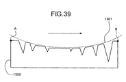
- Fig. 39 is a cross-section of a workpiece with a flat plate on which fine V-shaped grooves are formed by a conventional technology.
- the machining process is started at position A of the flat plate 1300, and finished at position B.
- the servo mechanism of the machining device is affected by any disturbance such as temperature, atmospheric pressure, or vibration
- the surface of the machining side is formed into a curved surface as shown by a dot line 1301. Therefore, when the servo mechanism is affected by an external environment (disturbance), it becomes difficult to form a desired shape with sufficient precision.
- This kind of problem becomes more conspicuous when a fine-shape element has not a simple shape, but an irregular shape.
- the present invention is to solve the above problems.
- the object of the present invention is to provide a spatial light modulator and a projector that provide smooth image quality without the light-shielding area, such as the black matrix, being recognized.
- another object of the present invention is to provide a process for manufacturing a microstructure element with a desired fine-shape accurately independent of the external environment, a microstructure element manufactured by the process, a spatial light modulator employing the microstructure, and a projector employing the spatial light modulator.
- a spatial light modulator includes a modulating unit that modulates incident light based on an image signal, and outputs modulated light, and a refracting unit that is disposed on an output-side of the modulating unit, and refracts the light from the modulating unit.
- the modulating unit includes a plurality of pixels arranged in a matrix format, and a light-shielding part placed between the pixels.
- the refracting unit includes a group of prisms formed with a prism element that has at least a refracting surface. Light from one of the pixels is incident on at least a part of the group of prisms.
- a direction of the refracting surface is such that a projection image of the pixels is guided onto a projection image of the light-shielding part on a projection surface at a predetermined distance from the refracting unit.
- the refracting surface and a reference surface that is formed in a direction perpendicular to an optical axis make a predetermined angle.
- a projection image of a pixel formed by refracted light on a projection surface placed apart from the refracting unit by a predetermined distance, is directed onto a projection image of a light-shielding part.
- an area of one prism element of the group of prisms is defined as a unit area
- a ratio between an area of the refracting surface and the unit area corresponds to light intensity of the projection image of the pixels.
- Light released from a pixel is formed into divergence lights having a cone shape, and made incident on a group of prisms consisting of multiple prism elements.
- the region area of one prism element is made to be a unit area that forms a standard.
- a value obtained by dividing the area of a specific refracting surface by the unit area, that is, an area ratio, corresponds to a ratio between quantity of incident light per unit area and quantity of light refracted by the specific refracting surface.
- the quantity of light to be refracted by a refracting surface can be controlled by properly setting the area of the refracting surface.
- the pixels are in a substantially rectangle shape; the light-shielding part is in a band shaped having a predetermined width arranged in a lattice form; and the group of prisms is constituted by prism elements having a polygonal cone shape.
- the group of prisms is constituted by prism elements having a polygonal cone shape.
- pixels of the rectangle shape are arranged in a crisscross matrix form.
- a light-shielding part such as a black matrix is placed in an area between the adjacent pixels.
- the prism element is made to be a polygonal cone shape, it becomes possible to set the direction of the refracting surface to various directions.
- the projection image of the pixel can be formed in various directions.
- the angle and area of the refracting surface are also desirably set. Consequently, the position and the quantity of light of the projection image of the pixel can be controlled.
- the polygonal cone shape in addition to a cone shape with a polygonal bottom shape, "the polygonal cone shape” also includes a cone shape having a flat face portion near the apex of the cone shape.
- the group of prisms is constituted by prism elements having a virtually pyramid shape.
- the prism element By allowing the prism element to have a pyramid shape, it is possible to form the projection image of the pixel in the direction orthogonal to bottom sides of the prism element.
- the pixel has the rectangle shape, it becomes possible to more efficiently form the projection image of the pixel in a superposed manner with respect to the projection image of the light-shielding part.
- the pixels are in a substantially rectangle shape; the light-shielding part is in a band shaped having a predetermined width arranged in a lattice form; the group of prisms is constituted by two sets of prism elements that have a cross-section of a virtually trapezoidal shape in a first direction with a longitudinal direction in a second direction that is virtually perpendicular to the first direction; the two sets of prism elements are arranged in such a manner that the longitudinal directions are virtually at right angles to each other; and a slope of the trapezoidal shape corresponds to the refracting surface.
- the cross-sectional shape in the first direction of the prism element is set to a virtually trapezoidal shape.
- the slope of the trapezoidal shape serves as a refracting surface. For this reason, the projection image of the pixel derived from light refracted by the slope can be formed in a direction orthogonal to the length direction of the prism element. Moreover, in the present aspect, the length directions of two sets of prism elements are made virtually orthogonal to each other. With this arrangement, when the pixel has the rectangle shape, it becomes possible to more efficiently form the projection image of the pixel in a superposed manner with respect to the projection image of the light-shielding part on the periphery of the pixel.
- the refracting unit further includes a flat portion virtually parallel to a surface on which the pixels are formed; and light transmitted through or reflected on the flat portion from among the light from the pixels propagates substantially straight to form the projection image.
- a light, which is made incident on the refracting surface of the prism element is refracted in accordance with the direction, angle and area of the refracting surface.
- the light that is made incident on the flat portion is allowed to proceed straight and transmitted without being refracted.
- the projection image of the pixel, formed by light that is allowed to proceed straight and transmitted through the flat portion is referred to as "direct transmission image”
- the projection image of the pixel, formed by light that is transmitted and refracted by the prism is referred to as "refracted transmission image”.
- prism elements that are assigned based upon not less than one area ratio are placed within a swallowing angle that is defined by illumination light or the F number of the projection lens, at a front position in the light advancing direction from a point at which the light-shielding part is located on the space modulating element so that it becomes possible to obtain a pixel that is formed with a light-quantity ratio that is assigned based upon areas between the direct transmission image and refracted transmission image.
- the prism element has the direction of the refracting surface and the predetermined angle in such a manner that an intersection point of center lines of the projection image of the light-shielding part arranged in the lattice form is substantially coincident with one of corners of the projection image of the pixels.
- the prism element has the direction of the refracting surface and the predetermined angle in such a manner that at least parts of the projection images of adjacent pixels are overlapped on the projection image of the light-shielding part.
- the prism element has the direction of the refracting surface and the predetermined angle in such a manner that substantially entire areas of the projection images of adjacent pixels are overlapped on the projection image of the light-shielding part.
- a sum of intensities of light from the flat portion on the projection surface PW0 and a sum of intensities of light through the refracting surface on the projection surface PW1 satisfy an inequality PW0 ⁇ PW1.
- the sum of the light intensities of a direct transmission image corresponds to the area of the flat portion.
- the sum of the light intensities of a refracted transmission image corresponds to the area of the refracting surface.
- the refracted transmission image is formed on the periphery of the direct transmission image.
- the arrangement is made so as to satisfy PW0 ⁇ PW1.
- PW0>PW1 is preferably satisfied. More preferably, an inequality, PW0>0.9 ⁇ PW1, is satisfied.
- a first peak of intensity distribution of the projection images of the pixels formed by light from the flat portion is bigger than a second peak of intensity distribution of the projection images of the pixels formed by light through the refracting surface; and light intensity of an area between the first peak and the second peak corresponds to a predetermined intensity distribution curve.
- a projector includes a light source that supplies a first-color light, a second-color light, and a third-color light, a first-color spatial light modulator that modulates the first-color light based on an image signal, a second-color spatial light modulator that modulates the second-color light based on the image signal, a third-color spatial light modulator that modulates the third-color light based on the image signal, a color-synthesizing optical system that synthesizes the first-color light, the second-color light, and the third-color light, modulated by the first-color spatial light modulator, the second-color spatial light modulator, and the third-color spatial light modulator, respectively, and a projection lens that projects light synthesized by the color-synthesizing optical system.
- the first-color spatial light modulator, the second-color spatial light modulator, and the third-color spatial light modulator are the spatial light modulator according to the one aspect of the present invention.
- solid-state light-emitting elements such as light-emitting diodes and semiconductor lasers, that respectively supply the first color light, second color light and third color light may be used as a light source.
- a projection image of the pixel is formed on an area of a projection image of the light-shielding part in a superposed manner. Therefore, in the screen, the viewer is allowed to view an image that is smooth, and less susceptible to roughened texture, without recognizing an image of the light-shielding part.
- each of the first-color spatial light modulator, the second-color spatial light modulator, and the third-color spatial light modulator includes the refracting unit.
- the angle at which light is refracted by the refracting surface is dependent on the light wavelength. For example, when a plurality of lights having different wave-length ranges are made incident on the same refracting surface, refracted angles are different depending on the respective wave-length ranges.
- the first-light-color-use spatial light modulator, the second-light-color-use spatial light modulator and the third-light-color-use spatial light modulator are respectively provided with the refracting units.
- the refracting unit is disposed on incident side or output-side of the color-synthesizing optical system.
- one refracting unit may be installed on the incident side or the output-side of a color synthesizing optical system such as a cross dichroic prism.
- the projector further includes a color-separation optical system that separates light supplied from the light source into the first-color light, the second-color light and the third-color light.
- the light source supplies light within all the wavelength ranges including the first, second and third color lights.
- light from the light source is separated by the color separation optical system into the first color light, the second color light and the third color light so that the respective lights can be modulated in accordance with image signals.
- a method of manufacturing a microstructure element includes dividing a machining area into five or more sub-areas, forming a first shape in any one of the sub-areas, forming a second shape at another sub-area that is located farther from the any one of the sub-areas than an adjacent area to the any one of the sub-areas, taking the any one of the sub-areas as a new reference, and repeating the forming a second shape, taking the another sub-area on which the second shape is formed as the new reference.
- the machining position is continuously shifted from the position at which the machining process is started so that the machining process such as cutting is successively carried out.
- the adverse effects from external disturbance, as they are, tend to be reflected to the results of the machining process.
- the machining area is first divided into a plurality of sub-machining areas, that is, for example, five or more machining areas. Next, a first shape is formed in a desired one of the sub-areas.
- a second shape is formed at another sub-area that is not adjacent to the sub-area on which the first shape is formed, and located at a position apart from the sub-area by a distance corresponding to at least one sub-area.
- the second shape is formed at still another sub-area that is not adjacent to the sub-area on which the second shape is formed, and located at a position apart from the sub-area by a distance corresponding to at least one sub-area.
- the first shape and the second shape are substantially same shape.
- the first shape and the second shape are different from each other.
- the method further includes forming the first shape, based on machining data, on a trial machining area that is different from the machining area, measuring the first shape formed on the trial machining area, compensating the machining data by performing a feedback of a difference between measured data and the machining data to the machining data, and repeating the forming the first-shape based on the machining data compensated.
- the fine-shape element is formed based upon machining data. Then, since the shape is not formed as defined by the machining data because of influences from disturbance and defective setting of the relative position between the machining cutting tool and the workpiece, a failure occurs in obtaining a desired machining precision.
- the machined first shape is preliminarily measured actually.
- an atomic force microscope and a laser microscope are preferably used.
- the measurement data of the measured fine-shape element are compared with the original machining data so that a finite difference between the two kinds of data is calculated.
- the finite difference, thus calculated, is fed back to the machining data.
- the first-shape forming process and the repeating process are carried out. Consequently, it becomes possible to carry out a shape-machining process that is less susceptible to influences from disturbance and the like.
- the forming the first shape on a trial machining area, forming a first shape in any one of the sub-areas, and the repeating the forming the first-shape are performed at same position at least two times.
- a fine shape is machined by changing the angle of a cutting tool at the same position, it is possible to obtain a desired fine shape.
- the measuring includes measuring at least one of factors including pitch, angle, depth and, flat surface roughness of the first shape.
- factors including pitch, angle, depth and, flat surface roughness of the first shape.
- a microstructure element is manufactured by using the method according to the above aspect. With this arrangement, it becomes possible to manufacture a microstructure element having a single shape or an irregular shape, such as a group of prisms constituted by multiple micro-prism elements.
- a spatial light modulator includes the microstructure element according to the above aspect.
- a transmission-type liquid-crystal-type spatial light modulator has a group of prisms constituted by micro-lens elements.
- the direction of outgoing light is accurately refracted in a predetermined direction to be deflected.
- light released from pixels can be refracted and directed to a projection image of the black matrix located between pixels of the spatial light modulator. Consequently, it becomes possible to obtain an image with high quality, without allowing the viewer to recognize the black matrix.
- a projector includes a light source that supplies illuminating light, the spatial light modulator according to the above aspect that modulates the illuminating light based on an image signal, and a projection lens that projects modulated light.
- the space light modulating device since the space light modulating device is installed, it is possible to provide a projection image with high quality.
- an extra-high pressure mercury lamp 101 which serves as a light source, supplies light containing red light (hereinafter, referred to as "R-light”) that is the first color light, green light (hereinafter, referred to as "G-light”) that is the second color light and blue light (hereinafter, referred to as "B-light”) that is the third color light.
- R-light red light
- G-light green light
- B-light blue light
- An integrator 104 equalizes the illuminance distribution of light from the extra-high pressure mercury lamp 101.
- the light, equalized in its illuminance distribution, is converted by a polarized light conversion device 105 into polarized light with a specific vibration direction, that is, for example, s-polarized light.
- the light, converted to s-polarized light is made incident on an R-light transmission dichroic mirror 106R that forms a color separation optical system.
- the following description will discuss the R-light.
- the R-light transmission dichroic mirror 106R transmits the R-light, and reflects the G-light and B-light.
- the R-light, transmitted through the R-light transmission dichroic mirror 106R, is made incident on a reflection mirror 107.
- the reflection mirror 107 bends the light path of the R-light by 90 degrees.
- the R-light with its light path bent is made incident on a first-color spatial light modulator 110R that modulates the R-light that is the first-color light in accordance with an image signal.
- the first-color spatial light modulator 110R is a transmission-type liquid crystal display that modulates the R-light in accordance with an image signal.
- the polarizing direction of the light is not changed even after the transmission through the dichroic mirror, the R-light to be made incident on the first-color spatial light modulator 110R is still maintained as the s-polarized light.
- the first-color spatial light modulator 110R is provided with a ⁇ /2 phase difference plate 123R, a glass plate 124R, a first polarizing plate 121 R, a liquid crystal panel 120R and a second polarizing plate 122R.
- the structure of the liquid crystal panel 120R will be described later in detail.
- the ⁇ /2 phase difference plate 123R and the first polarizing plate 121 R are placed so as to be made contact with a light-transmitting glass plate 124R that does not change the polarizing direction.
- the second polarizing plate 122R is placed in an independent manner; however, this may be placed so as to be made in contact with the outgoing face of the liquid crystal panel 120R and the incident face of the cross dichroic prism 112.
- the s-polarized light, made incident on the first-color spatial light modulator 110R, is converted into p-polarized light by the ⁇ /2 phase difference plate 123R.
- the R-light converted into the p-polarized light is allowed to pass through the glass plate 124R and the first polarizing plate 121 R as it is, and made incident on the liquid crystal panel 120R.
- the p-polarized light, made incident on the liquid crystal panel 120R is subjected to a modulating process in accordance with an image signal so that the R-light is converted to s-polarized light.
- the R-light that has been converted to the s-polarized light through the modulating process of the liquid crystal panel 120R is released from the second polarizing plate 122R. In this manner, the R-light that has been modulated by the first-color spatial light modulator 110R is made incident on the cross dichroic prism 112 that is a color-synthesizing optical system.
- the G-light The G-light and B-light, reflected by the R-light transmission dichroic mirror 106R, have their light paths bent by 90 degrees.
- the G-light and B-light with their light paths bent are made incident on a B-light transmission dichroic mirror 106G.
- the B-light transmission dichroic mirror 106G reflects the G-light, and transmits the B-light.
- the G-light that has been reflected by the B-light transmission dichroic mirror 106G is made incident on a second-color spatial light modulator 110G that modulates the G-light that is the second-color light in accordance with an image signal.
- the second-color spatial light modulator 110G is a transmission-type liquid crystal display that modulates the G-light in accordance with an image signal.
- the second-color spatial light modulator 110G is provided with a liquid crystal panel 120G, a first polarizing plate 121 G and a second polarizing plate 122G.
- the structure of the liquid crystal panel 120G will be described later in detail.
- the G-light to be made incident on the second-color spatial light modulator 110G is converted into s-polarized light.
- the s-polarized light, made incident on the second-color spatial light modulator 110G is allowed to pass through the first polarizing plate 121G as it is, and made incident on the liquid crystal panel 120G.
- the s-polarized light, made incident on the liquid crystal panel 120G is subjected to a modulating process in accordance with an image signal so that the G-light is converted to p-polarized light.
- the G-light that has been converted to the p-polarized light through the modulating process of the liquid crystal panel 120G is released from the second polarizing plate 122G. In this manner, the G-light that has been modulated by the second-color spatial light modulator 110G is made incident on the cross dichroic prism 112 that is a color-synthesizing optical system.
- the B-light that has passed through the B-light transmission dichroic mirror 106G is made incident on a third-color spatial light modulator 110B that modulates the B-light that is the third-color light in accordance with an image signal, after passing through two relay lenses 108 and two reflection mirrors 107.
- the third-color spatial light modulator 110B is a transmission-type liquid crystal display that modulates the B-light in accordance with an image signal.
- the reason that the B-light is allowed to pass through the relay lenses 108 is because the light path of the B-light is longer than the light paths of the R-light and G-light.
- the B-light that has passed through the B-light transmission dichroic mirror 106G, as it is, is directed to the third-color spatial light modulator 110B.
- the third-color spatial light modulator 110B is provided with a ⁇ /2 phase difference plate 123B, a glass plate 124B, a first polarizing plate 121B, a liquid crystal panel 120B and a second polarizing plate 122B.
- the structure of the third-color spatial light modulator 110B is the same as that of the first-color spatial light modulator 110R; therefore, the detailed description thereof is omitted.
- the B-light to be made incident on the third-color spatial light modulator 110B is converted into s-polarized light.
- the s-polarized light, made incident on the third-color spatial light modulator 110B is converted into p-polarized light by the ⁇ /2 phase difference plate 123B.
- the B-light converted into the p-polarized light is allowed to pass through the glass plate 124B and the first polarizing plate 121B as it is, and made incident on the liquid crystal panel 120B.
- the p-polarized light, made incident on the liquid crystal panel 120B is subjected to a modulating process in accordance with an image signal so that the B-light is converted to s-polarized light.
- the B-light that has been converted to the s-polarized light through the modulating process of the liquid crystal panel 120B is released from the second polarizing plate 122B.
- the B-light that has been modulated by the third-color spatial light modulator 110B is made incident on the cross dichroic prism 112 that is a color-synthesizing optical system.
- the R-light transmission dichroic mirror 106R and the B-light transmission dichroic mirror 106G which constitute a color-separation optical system, separate light supplied from the extra-high pressure mercury lamp 101 into the R-light serving as the first-color light, the G-light serving as the second-color light and the B-light serving as the third-color light.
- the cross dichroic prism 112 serving as a color-synthesizing optical system is constituted by two dichroic films 112a and 112b that are orthogonally placed in an X-letter form.
- the dichroic film 112a reflects the B-light, and transmits the R-light and G-light.
- the dichroic film 112b reflects the R-light, and transmits the B-light and G-light.
- the cross dichroic prism 112 synthesizes the R-light, G-light and B-light that have been respectively modulated by the first-color spatial light modulator 110R, the second-color spatial light modulator 110G and the third-color spatial light modulator 110B.
- a projection lens 114 projects the light synthesized by the cross dichroic prism 112 onto a screen 116. Thus, a full-color image is obtained on the screen 116.
- the lights to be made incident on the cross dichroic prism 112 from the first-color spatial light modulator 110R and the third-color spatial light modulator 110B are formed into s-polarized light.
- the light to be made incident on the cross dichroic prism 112 from the second-color spatial light modulator 110G is formed into p-polarized light.
- lights released from the respective color-light-use spatial light modulators can be effectively synthesized by the cross dichroic prism 112.
- the dichroic films 112a and 112b are superior in the reflective property for the s-polarized light.
- the R-light and B-light to be reflected by the dichroic films 112a and 112b are formed into the s-polarized light, and the G-light that is allowed to pass through the dichroic films 112a and 112b is formed into the p-polarized light.
- the projector 100 explained in Fig. 1, is provided with three liquid crystal panels 120R, 120G and 120B. These three liquid crystal panels 120R, 120G and 120B have the same basic structure except that they have different light wavelength ranges to be modulated. Therefore, the following description will discuss the liquid crystal panel 120R as the typical example thereof.
- Fig. 2 is a schematic of the liquid crystal panel 120R.
- R-light released from the extra-high pressure mercury lamp 101, is made incident on the liquid crystal panel 120R from the lower side of Fig. 2, and released toward the screen 116 from the upper side thereof.
- An opposing substrate 202 having transparent electrodes and the like is formed inside an incident-side dust-preventive transparent plate 201.
- a thin film transistor (TFT) substrate 205 having TFTs, transparent electrodes and the like is formed inside an output-side dust-preventive transparent plate 206.
- TFT thin film transistor
- the opposing substrate 202 and the TFT substrate 205 are aligned face to face with each other, and the incident-side dust-preventive transparent plate 201 and the output-side dust-preventive transparent plate 206 are bonded to each other.
- a liquid crystal layer 204 which is used for displaying images, is sealed between the opposing substrate 202 and the TFT substrate 205.
- a black matrix layer 203 to be used for shielding light is installed on the incident-light side of the liquid crystal layer 204.
- a group of prisms 210 constituted by a plurality of prism elements 211, is formed on the output-side surface of the output-side dust-preventive transparent plate 206.
- the structure and functions of the group of prisms 210 will be described later.
- the first polarizing plate 121 R and the second polarizing plate 122R are installed on the liquid crystal panel 120R as separated members.
- a polarizing plate may be formed between the incident-side dust-preventive transparent plate 201 and the opposing substrate 202 as well as between the output-side dust-preventive transparent plate 206 and the TFT substrate 205.
- the group of prisms 210 may be formed either on the second polarizing plate 122R, or on the R-light incident face of the cross dichroic prism 112.
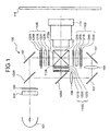
- Fig. 3 is a schematic of the black matrix layer 203.
- a black matrix 220 which forms a light-shielding part, shields the R-light that has been made incident thereon from the extra-high pressure mercury lamp 101 so that no light is released toward the screen 116 side.
- the black matrix 220 is formed in a lattice shape in the orthogonal directions with predetermined widths W1 and W2.
- a rectangular area surrounded by the black matrix 220 forms an opening section 230.
- the opening section 230 transmits the R-light from the extra-high pressure mercury lamp 101.
- the R-light that has been transmitted through the opening section 230 is allowed to pass through the opposing substrate 202, the liquid crystal layer 204 and the TFT substrate 205, as shown in Fig. 2.
- the polarized light components of the R-light are modified by the liquid crystal layer 204 in accordance with an image signal.
- the lights which have been transmitted through the opening section 230, the liquid crystal layer 204 and the TFT substrate 205 and modulated, are allowed to form a pixel in a projected image. Since the lights have been transmitted through the opening section 230, the position and size of the opening section 230 respectively correspond to the position and size of the pixel.
- the center line CL of the band-shaped black matrix 220 is indicated by a dashed line.
- periodic area 240 an area, surrounded by the center line CL and indicated by a bold line in the Figure, is referred to as periodic area 240.
- the adjacent periodic areas 240 are arranged periodically without clearance in a repeated manner.
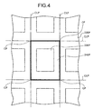
- Fig. 4 is a schematic of an image projected onto the screen 116 by a conventional projector in an enlarged manner.
- An image of an opening section 230P is projected in such a manner that it is surrounded by a band-shaped black matrix image 220.
- a periodic area image 240P shown as an area surrounded by the bold line in Fig. 4, is projected.
- the position where center line images CLP intersect with each other is defined as an intersection point CP.
- explanations are given by using images projected on the screen 116 by the projection lens 114. In the case when only the first-light-use spatial light modulator 110R is taken out to be considered, no projection lens 114 is present.
- the projection images are dealt as images that are projected on an imaginary projection plane that is apart from the group of prisms 210 serving as a refracting unit by a predetermined distance.
- the projection image formed by the projector 100 and the projection image formed by the single first-color spatial light modulator 110R are virtually the same image except that the image magnification is different from each other. For this reason, the following explanation will be given by reference to projected images on the screen 116.
- Fig. 5 is a cross-section of the liquid crystal panel for illustrating a relation between the black matrix layer 203 and the group of prisms 210 serving as a refracting unit.
- the R-light that has passed through the opening section 230 corresponding to a pixel is formed into divergence lights having a cone shape, and allowed to progress. Further, the R-light is made incident on at least one portion of the group of prisms 210.
- the group of prisms 210 is constituted by prism elements 211 each of which is provided with at least a refracting surface 212 and a flat portion 213.
- the flat portion 213 is a face that is virtually in parallel with a face 230a in which the opening section 230 corresponding to the pixel is formed.
- Multiple prism elements 211 are regularly arranged with a fixed cycle so that the group of prisms 210 is formed.
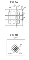
- Fig. 6A, Fig. 6B, and Fig. 6C are plan views that show a positional relationship between the opening section 230 and the group of prisms 210.
- each of the prism elements 211 has a virtually square shape.
- the direction of the center line CL of the black matrix layer 203 shown in Fig. 6A and the direction of the side 211 a of each prism element 211 shown in Fig. 6B are made to form an angle of about 45°.
- the light that has passed through one opening section 230 is made incident on one portion of the group of prisms 210 constituted by multiple prism elements 211.
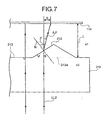
- Fig. 7 is an enlarged view of proximity of the group of prisms 210 that forms a refracting unit.
- the medium for example, air
- the constituent member of the group of prisms 210 is set to a refractive index n2.
- the refracting surface 212 is formed so as to have an angle ⁇ with respect to a reference plane 213a formed by extending the flat portion 213.
- the angle ⁇ is referred to as tilt angle.
- the distance S that corresponds to the movement of the opening section image 230P on the screen 116 can be desirably set.
- the direction at which a light LL2 is refracted is dependent on the direction of the refracting surface 212.
- the direction in which the opening section image 230P is formed on the screen 116 can be desirably set.
- a side of the square prism element 211 has a length La
- one side of the flat portion 213 has a length Lb.
- an area La ⁇ La that is occupied by one prism element 211 is set to a unit area.
- four refracting surfaces 212a, 212b, 212c and 212d have respective areas of P1, P2, P3 and P4.
- the quantity of light that is transmitted through the flat portion 213 and proceeds straight corresponds to the area FS of the flat portion 213 that accounts for the unit area.
- the total quantity of lights that are refracted by the four refracting surfaces 212a, 212b, 212c and 212d corresponds to the total area P1+P2+P3+P4 of the four refracting surfaces 212a, 212b, 212c and 212d that accounts for the unit area.
- the quantity of light that is allowed to pass straight through or refracted by the prism element 210 is desirably set on the screen 116.
- the quantity of light of a projection image (direct transmission image) that is transmitted through the flat portion 213 and proceeds straight and the quantity of light of a projection image that is refracted by the refracting surface 212 are preferably made equal to each other.
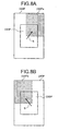
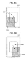
- Fig. 8A shows a periodic area image 240P on the screen 116.
- Lights that have been virtually perpendicularly made incident on the flat portion 213 of the prism element 211 are allowed to proceed straight, without being subjected to the refracting function in the flat portion 213.
- the straight proceeding lights form an opening section image (direct transmission image) 230P in the center of the periodic area 240P on the screen 116.
- the lights that have been made incident on the refracting surface 212a are subjected to refracting functions so as to have the refracting direction, the quantity of refraction and the quantity of refracted light that correspond to the direction of the refracting surface 212a, the tilt angle ⁇ and the area P1.
- the direction of the side 211a of the prism element 211 and the direction of the center line CL of the black matrix layer 203 are made to form an angle of about 45°. For this reason, for example, as shown in Fig.
- the lights that are refracted by the refracting surface 212a are allowed to form an opening section image 230Pa at a position apart from the opening section image (direct transmission image) 230P by the distance S in the direction of arrow.
- the viewer should always observe in the viewing direction of the extra-high pressure mercury lamp 101 serving as the light source.
- the image, projected on the screen 116 should be observed in the viewing direction of the extra-high pressure mercury lamp 101 (oncoming direction of light) from the rear side of the screen 116.
- the lights that have been refracted by the refracting surface 212b are allowed to form an opening section image 230Pb at a position shown in Fig. 8B.
- the lights that have been refracted by the refracting surface 212c are allowed to form an opening section image 230Pc at a position shown in Fig. 8C.
- the lights that have been refracted by the refracting surface 212d are allowed to form an opening section image 230Pd at a position shown in Fig. 8D.
- Fig. 8A to Fig. 8D explain the respective opening section images 230Pa, 230Pb, 230Pc and 230Pd in a separate manner.
- these four opening section images 230Pa, 230Pb, 230Pc and 230Pd are projected in a superposed manner as shown in Fig. 9.
- the refracting surface 212 has the direction of the refracting surface 212 and the tilt angle ⁇ in such a manner that the opening section images 230Pa, 230Pb, 230Pc and 230Pd corresponding to the pixels are directed onto the black matrix image 220P that is the projection image of the black matrix 220 serving as the light-shielding part on the screen 116 that is a projection (receiving) face located apart from the group of prisms 210 by the predetermined distance L serving as the refracting unit.
- the opening section images 230Pa, 230Pb, 230Pc and 230Pd are formed in the area of the black matrix image 220P in a superposed manner. Therefore, this arrangement makes it possible to prevent the viewer from recognizing the black matrix image 220P.
- each prism element 211 has such a direction of the refracting surface 212 and a tilt angle ⁇ of the refracting surface 212 that each of the intersection points CPa, CPb, CPc and CPd of the center line image CLP of the black matrix images 220P that are light-shielding part images arranged in a lattice form is made virtually coincident with the corresponding one of the corner portions of the opening section image (direct transmission image) 230P of the opening section 230 that forms a pixel. For this reason, it is possible to obtain a so-called seamless image that is less susceptible to blurring between pixels, that is, a smooth image that is less susceptible to roughened texture.
- the group of prisms 210 is integrally formed on the outgoing face of the output-side dust-preventive transparent plate 206.
- the output-side dust-preventive transparent plate 206 is constituted by transparent parallel glass flat plates.
- a group of prisms 210 is formed on one of the faces of the transparent parallel glass flat plates by using the photolithography technique. More specifically, a photoresist layer is patterned on the parallel flat glass plate so as to have a desired prism shape, for example, a pyramid shape, by using a gray scale method so that a mask is formed.
- the group of prisms 210 may be formed by using a wet-etching method in which hydrofluoric acid is used.
- the output-side dust-preventive transparent plate 206 constituted by the parallel glass flat plates one of the faces of which has the group of prisms 210, is formed on the outermost output-side in the manufacturing processes of the liquid crystal panel 120R.
- the pattern-transferring process another method may be adopted.
- the parallel flat glass plates are heated to such a softened state required for the mold-transferring process. Then, by pressing the mold onto one of the faces of the parallel flat glass plates that has been softened, the pattern-transferring process is carried out. With this method also, the group of prisms 210 is formed on the parallel flat glass plates.
- the formation of the group of prisms 210 is not limited to a structure in which the group is integrally formed with the output-side dust-preventive transparent plate 206.
- a group of prisms 210 having a desired prism shape is preliminarily manufactured as a pattern sheet through a hot-pressing method in a separate manner. Then, the pattern sheet is properly cut into a required size. Next, the pattern sheet thus cut is affixed onto the outgoing-face side of the parallel glass flat plates by using an optically transparent bonding agent. With this method also, the group of prisms 210 can be formed on the parallel flat glass plates.
- a coating layer made from a transparent resin or the like having a low refractive index, is formed on the output-side face of the group of prisms 210.
- the refractive index of a member to be used for forming the group of prisms 210 may be virtually coincident with the refractive index of the coating layer. With this arrangement, it is possible to reduce positional offsets of refracted lights on the screen 16 caused by deviations in manufacturing errors of the refracting surface 212.
- the size of the prism element 211 a distributed based upon the area ratio is virtually included inside the diameter ⁇ , and by making the ratio of the flat portion area and each of the prism angle projection areas virtually coincident with a designed value inside the diameter ⁇ , it is possible to obtain pixels that are composed based upon the ratio of quantities of light that are assigned in association with the areas of the direct transmission image and the refracted transmission image.
- the R-light is explained as a typical example.
- the basic structure is also the same as the case of the R-light. More specifically, each of the first-color spatial light modulator 110R, the second-color spatial light modulator 110G and the third-color spatial light modulator 1108 is provided with the group of prisms 210 that serves as a refracting unit.
- the refracted angle derived from the refracting surface 212 is different depending on the wavelengths of light. For this reason, in an attempt to accurately control the position of the image that is diffracted and projected on the screen 116, it is preferable to take the wavelength of light to be refracted into consideration.
- the extra-high pressure mercury lamp 101 serving as the light source has a light-emission spectrum distribution shown in Fig. 10.
- the axis of abscissas indicates the wavelength
- the axis of ordinates indicates the predetermined unit of strength.
- the B-light light that has a peak wavelength in the bright line spectrum virtually in the vicinity of 440 nm is used as the B-light
- light that has a peak wavelength virtually in the vicinity of 550 nm is used as the G-light
- light that has a peak wavelength virtually in the vicinity of 650 nm that is the center wavelength of the light quantity integrated value is used as the R-light.
- the tilt angle ⁇ and the like of the refracting surface 212 are controlled so that, when lights having these wavelengths are refracted by the refracting surface 212, a predetermined projection image is formed on the screen 116. With this arrangement, it is possible to obtain an image with high quality that is less susceptible color offsets on the screen 116.
- the optimal height (depth) H is about 45.5 ⁇ m.
- the group of prisms 210 is formed on the output-side face of each of the liquid crystal panels 120R, 120G and 120B, for example, on a quartz substrate face
- numerical examples are given as follows with respect to the tilt angle ⁇ of the prism element 211.
- the tilt angles ⁇ of the respective prism elements 211 for the R-light, G-light and B-light are respectively set to 0.31°, 0.31° and 0.30°.
- the reason that the tilt angles are different among the respective colors is because, as described earlier, the refractive indexes of the members constituting the group of prisms 210 are different depending on wavelengths.
- the tilt angles ⁇ of the respective prism elements 211 for the R-light, G-light and B-light are set to 0.10°, 0.10° and 0.099° respectively.
- the tilt angle ⁇ is a small value, it is sometimes difficult to form the group of prisms 210 by using, for example, a cutting process. Therefore, a material having a refractive index close to the refractive index of the members forming the group of prisms 210 is formed on the interface of the group of prisms 210 through a molding process.
- a difference in refractive indexes between the members forming the group of prisms 210 and the material to be molded is 0.3.
- the tilt angles ⁇ of the R-light, G-light and B-light are respectively set to 1.16°, 1.17° and 1.18°.
- the tilt angles ⁇ of the respective prism elements 211 for the R-light, G-light and B-light are set to 0.31°, 0.31° and 0.31°.
- Fig. 11 is a schematic of a projector 1100 according to a second embodiment of the present invention.
- those parts that are the same as those of the first embodiment are indicated by the same reference numerals, and overlapping explanations are omitted.
- a group of prisms 1110 serving as a refracting unit is formed on the output-side face of a cross dichroic prism 112 that serves as a color composite optical system.
- Fig. 12 is an enlarged view of the cross dichroic prism 112.
- a group of prisms 1110 On the output-side face of the cross dichroic prism 112 toward the screen 116, a group of prisms 1110, having a structure as described below, is formed by using any one of the manufacturing methods. With this arrangement, since only one group of prisms 1110 is required, the structure is made simpler, making it possible to cut production costs.
- the group of prisms 1110 may be installed on the incident-side face of the cross dichroic prism 112. Since this arrangement makes it possible to set the refractive angles that correspond to the respective wavelengths, and consequently to optimize the refracted image.
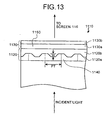
- Fig. 13 is a cross-section of the group of prisms 1110 cut along a line A-A shown in Fig. 12.
- the group of prisms 1110 is constituted by a first refractive layer 1120 and a second refractive layer 1130 placed on the output-side of the first refractive layer.
- Prism elements 1140 and 1150 are formed on the first refractive layer 1120 and second refractive layer 1130 respectively.
- the prism element 1150 formed on the second refractive layer 1130 since only the cross-section along the length direction is viewed, with the shape of the refracting surface being not illustrated.
- the following description will discuss a process for manufacturing the prism elements 1140 and 1150.
- the optical epoxy resin is irradiated with ultraviolet rays to be cured so that a lower-side high-refractive-index layer 1120a is formed.
- the surface of the optical epoxy resin thus applied is flattened by using a flattening squeegee.
- the optical epoxy resin is irradiated with ultraviolet rays to be cured so that a lower-side low-refractive-index layer 1120b is formed.
- an appropriate amount of an optical epoxy resin having a high refractive index is applied onto the lower-side low-refractive-index layer 1120b.
- concave and convex portions having a virtually sine-wave form that corresponds to the shape of the prism element 1150 that extends in the lateral direction on the face of the drawing are formed by using a squeegee.
- the optical epoxy resin is irradiated with ultraviolet rays to be cured so that an upper-side high-refractive-index layer 1130a is formed.
- an appropriate amount of optical epoxy resin having a low refractive index is applied on this upper-side high-refractive-index layer 1130a.
- the surface of the optical epoxy resin thus applied is flattened by using a flattening squeegee.
- the optical epoxy resin is irradiated with ultraviolet rays to be cured so that an upper-side low-refractive-index layer 1130b is formed.
- the optical epoxy resin having a high refractive index preferably has such a degree of viscosity that is required for maintaining the concave and convex shape of the predetermined prism element.
- the optical epoxy resin having a low refractive index preferably has a low viscosity that allows a flattening process.
- the lower-side low-refractive-index layer 1120b and the upper-side low-refractive-index layer 1130b may be formed by using a spin-coating method, a spray-coating method or the like.
- the group of prisms 1110 may have the same structure as the group of prisms 210 according to the first embodiment.
- a pattern corresponding to a shape of the prism element is preliminarily formed on a pattern sheet by using a hot-plate method or the like. Then, the pattern sheet is cut into an appropriate size required. The pattern sheet thus cut is affixed on the outgoing-face side of the cross dichroic prism 112 by using an optically transparent bonding agent.
- a projection image as shown in Fig. 9 is obtained on the screen 116.
- the prism element 1140 has a virtually sine-wave shape, the quantity of light that is allowed to proceed straight without being refracted and the quantity of light that is refracted are made to have a 1 to 1 ratio, that is, to be equal to each other.
- the optimal height (depth) of the prism element 1140 may be set to 45.5 ⁇ m.
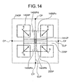
- Fig. 14 is a schematic of a projection image on the screen 116, which is formed by a projector according to the third embodiment.
- the present embodiment is different from the first embodiment and the second embodiment in the directions of the refracting surfaces, the tilt angles ⁇ and the area ratios of the prism elements 211, 1140, and 1150.
- various combinations among the directions of the refracting surfaces, the tilt angles ⁇ and the area ratios will be mainly explained.
- projection images according to the present embodiment include an opening section image 1400P (direct transmission image) derived from light that is allowed to proceed straight without being refracted by the flat portions of the prism elements 1140, 1150, and opening section images 1400Pa, 1400Pb, 1400Pc and 1400Pd that are formed at positions that are respectively apart from the opening section image 1400P by a distance S in each of the directions with 45° indicated by arrows.
- the inside of the periodic area image 240P is filled with the opening section images without any clearance.
- the present embodiment is characterized in that at least one portion among the adjacent four opening section images 1400Pa, 1400Pb, 1400Pc and 1400Pd is overlapped on the black matrix image 220P so that a new opening section image 1410P is formed.
- the new opening section image 1410P which is an area formed by overlapped portions of the adjacent pixel images 1400P, is allowed to newly form a third opening section image based upon image information derived from at least the adjacent first opening section image 1400Pa and second opening section image 1400Pb. Consequently, it is possible to improve the density of the number of pixels to be projected.
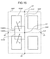
- Fig. 15 is a schematic of a projection image on the screen 116, which is formed by a projector according to the fourth embodiment.
- projection images according to the present embodiment include, for example, an opening section image 1500P (direct transmission image) derived from light that is allowed to proceed straight without being refracted by the flat portions of the prism elements 1140, 1150, and opening section images 1500Pa and 1500Pd that are formed at positions that are respectively apart from the opening section image 1500P by a distance S in each of the directions with 45° indicated by arrows.
- the inside of the periodic area image 240P is filled with the opening section images without any clearance.
- the present embodiment is characterized in that virtually entire areas of the adjacent two opening section images 1500Pa and 1500Pd are overlapped on the black matrix image 220P so that a new opening section image 1510P is formed.
- a third opening section image is newly formed based upon image information derived from the adjacent first opening section image 1500Pa and second opening section image 1500Pd. Consequently, it is possible to improve the density of the number of pixels to be projected.
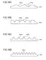
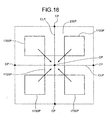
- Fig. 16A to Fig. 16D are cross-sections for illustrating various variations of the shape of a prism element.
- Fig. 16A shows a group of prisms 1610 having a trapezoidal shape having a refracting surface 1610a and a flat portion 1610b.
- Fig. 16B shows a group of prisms 1620 having a triangular shape having a refracting surface 1620a and a flat portion 1620b.
- Fig. 16C shows a group of prisms 1630 having a triangular shape having a refracting surface 1630a and a flat portion 1630b.
- Fig. 16A shows a group of prisms 1610 having a trapezoidal shape having a refracting surface 1610a and a flat portion 1610b.
- Fig. 16B shows a group of prisms 1620 having a triangular shape having a refracting surface 1620a and a flat portion 1620b.
- 16D shows a group of prisms 1640 of a braze type that is formed by only a refracting surface 1640a. In these manners, various variations are prepared by using the direction of the refracting surface, the tilt angle and the area as parameters.
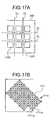
- Fig. 17A, Fig. 17B, and Fig. 17C are schematics for illustrating the positional relation between an opening section 1700 and a group of prisms 1710.
- directions along the respective sides 1711a of prism elements 1711 are arranged to form virtually 45° as shown in Fig. 17B.
- light that has passed through one opening section 1700 is made incident on one portion of a group of prisms 1710 constituted by a plurality of prism elements 1711.
- each of the prism elements 1711 has a virtually square shape.
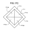
- the prism element 1711 has polygonal cone shape prism elements, that is, for example, pyramid-shaped refracting surfaces 1712a, 1712b, 1712c and 1712d.
- a flat portion 1713 is formed on the periphery of each of the refracting surfaces 1712a, 1712b, 1712c and 1712d.
- a projection image on the screen 116 will discuss a projection image on the screen 116 according to the present embodiment.
- Lights that have passed through the flat portion 1713 of the prism element 1711 are allowed to form opening section images (direct transmission image) 1700P.
- respective refracting surfaces 1712a, 1712b, 1712c and 1712d form opening section images 1720P that are projection images in the directions with 45° to the center line image CLP.
- the tilt angles of the respective refracting surfaces 1712a, 1712b, 1712c and 1712d are set in such a manner that four projection images from the four adjacent opening sections 1700 are overlapped at a position centered on the central intersection point CP of the four adjacent opening section images 1700P to form a new opening section image 1720P.
- the new opening section image 1720P is formed, the resolution on appearance can be improved to 1.25 times.
- the prism element 1711 has a unit area T. Further, the respective refractive interfaces 1712a, 1712b, 1712c and 1712d respectively have areas T/8, and the flat portion 1713 has an area 4T/8.
- the brightness of the respective projection images can be desirably set to, for example, virtually the same level as shown by the present embodiment. Thus, it becomes possible to obtain a smooth image.
- Fig. 19A, Fig. 19B, and Fig. 19C are schematics for illustrating the positional relation between an opening section 1900 and a group of prisms 1910.
- directions along the respective sides 1911 a of prism elements 1911 are arranged to form virtually 45° as shown in Fig. 19B.
- light that has passed through one opening section 1900 is made incident on one portion of a group of prisms 1910 constituted by a plurality of prism elements 1911.
- each of the prism elements 1911 has a virtually square shape.
- the prism element 1911 has polygonal cone shape prism elements, that is, for example, refracting surfaces 1912a, 1912b, 1912c and 1912d having a pyramid shape. Here, no flat portion is prepared.
- the respective refracting surfaces 1912a, 1912b, 1912c and 1912d form projection images in the directions with 45° to the center line image CLP.
- the tilt angles of the respective refracting surfaces 1712a, 1712b, 1712c and 1712d are set in such a manner that opening section images 1912Pa, 1912Pb, 1912Pc and 1912Pd, which are four projection images from the opening section 1900, are projected into the periodic area image 240P without being overlapped.
- the prism element 1911 has no flat portion. For this reason, no projection image (indicated by a dot line in Fig. 20) derived from components directly transmitted through the prism element 1911 is formed. In this manner, since no black matrix image is present, it becomes possible to obtain a seamless, smooth image.
- the prism element 1911 has a unit area T.
- the respective refractive interfaces 1912a, 1912b, 1912c and 1912d respectively have areas T/4.
- the opening section images 1912Pa, 1912Pb, 1912Pc and 1912Pd are respectively equal to one another to have a quantity of light that is proportional to the area T/4.
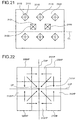
- Fig. 21 is an enlarged view of one portion of a group of prisms 2100 according to the seventh embodiment.
- This group of prisms 2100 is constituted by a first prism element 2110 having a pyramid shape and a second prism element 2120 having a pyramid shape.
- the first prism element 2110 is formed so that one side thereof is allowed to make virtually 45° to the center line CL.
- the second prism element 2120 is formed so that one side thereof is made virtually in parallel with the center line CL.
- a flat portion 2130 is formed on the periphery of each of the first prism element 2110 and the second prism element 2120.
- the following description will discuss a projection image on the screen 116 according to the present embodiment.
- Lights that have passed through the flat portion 2130 are allowed to form opening section images (direct transmission image) 2200P.
- the refracting surface 2111 of the first prism element 2110 forms an opening section image 2111P in a direction with 45° to the center line image CLP.
- the refracting surface 2121 of the second prism element 2120 forms an opening section image 2121 P in a direction parallel to the center line image CLP.
- the directions and tilt angles of the refracting surfaces are set so that the black matrix image is filled with these projection images without any clearance. Thus, it is possible to obtain a smooth image. It is also possible to provide a displaying process with double density.
- the area of the refracting surface 2111 is set to T/16
- the area of the refracting surface 2121 is set to 2T/16
- the area of the flat portion 2130 is set to 4T/16 respectively to the unit area T.
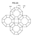
- the shape of the group of prisms that exert the same refracting functions as those according to the present embodiment can be modified in various manners.
- a group of prisms 2300 that has a refracting surface 2310 and a flat portion 2320 as shown in Fig. 23 may be used.
- Fig. 24 is a perspective cross-sectional view that shows a liquid crystal panel 120R of a spatial light modulator according to the eighth embodiment.
- the present embodiment is different from the first embodiment in the structure of a group of prisms 2400. Those parts that are the same as those according to the first embodiment are indicated by the same reference numerals and overlapping description is omitted.
- the group of prisms 2400 is secured to a TFT substrate 205 through a bonding layer 2401 on its incident side. Further, the group of prisms 2400 is secured to a cover glass plate 2403 through a bonding layer 2402 on its output-side.
- Fig. 25 is a schematic of the group of prisms 2400 according to the present embodiment.
- the refracting unit of the group of prisms 2400 is constituted by two sets of prism elements 2410a and 2410b.
- the prism element 2410a has a virtually trapezoidal shape in its cross-sectional shape in the y-axis direction that is the first direction.
- the length direction of the prism element 2410a corresponds to the x-axis direction that is the second direction virtually orthogonal to the y-axis direction that is the first direction.
- two slopes Y1 and Y2 function as refracting surfaces.
- an upper face Y0 serves as a flat portion.
- lights that have been made incident on the slope Y1 or the slope Y2 are refracted in a direction that corresponds to the angle of the slope.
- a refracted transmission image is formed by the refracted lights.
- lights that have been made incident on the upper face Y0 are transmitted as they are.
- the lights, transmitted as they are, are allowed to form a direct transmission image.
- the prism element 2410b has the same structure as that of the prism element 2410a. With respect to the cross-sectional shape in the x-axis direction of the prism element 2410b, two slopes X1 and X2 serve as refracting surfaces. Moreover, with respect to the cross-sectional shape in the x-axis direction of the prism element 2410b, an upper face X0 serves as a flat portion.
- the two sets of the prism elements 2410a and 2410b are arranged so that the respective length directions are virtually orthogonal to each other.
- the flat face side of the prism element 2410a and the flat face side of the prism element 2410b are secured so as to be aligned face to face with each other.
- any one of the following structures (1) to (3) may be used.
- Fig. 24 and Fig. 25 explain the structure in which the prism faces are made in contact with each other; however, another structure in which the prism faces are made in contact with air may be used.
- Fig. 26 is a schematic for illustrating the branched state of incident light by the group of prisms 2400.
- the incident light XY proceeds from left to right.
- lights are specified by using codes of slopes Y0, Y1 and Y2.
- the incident light XY are branched by the prism element 2410a indicated by a dot line into three lights, that is, lights Y1 and Y2 refracted by the slope and a light Y0 that is transmitted through the upper face as it is.
- Each of the three lights Y0, Y1 and Y2 is further branched by the prism element 2410b into three lights.
- the incident light XY is branched into nine lights Y1X1, Y1X0, Y1X2, Y0X1, Y0X0, Y0X2, Y2X1, Y2X0 and Y2X2.
- Fig. 27 positions of nine branched lights on a projection surface are explained.
- the area of the direct transmission image formed by the light Y0X0 is indicated by an area surrounded by a thick frame.
- Projection images, derived from the refracted lights, are formed in directions respectively orthogonal to the length directions of the prism elements 2410a and 2410b.
- the length directions of the two sets of the prism elements 2410a and 2410b are made virtually orthogonal to each other.
- a refracted transmission image is formed in an area between the direct transmission images derived from the light Y0X0, by the prism elements 2410a and 2410b.
- the sum of intensities of lights from the direct transmission image formed by the lights Y0X0 corresponds to the areas of the upper faces Y0 and X0 that form the flat portion. Further, the sum of intensities of lights from the refracted transmission image formed by the lights Y1X1, Y1X0, Y1X2, Y0X1, Y0X2, Y2X1, Y2X0 and Y2X2 corresponds to the areas of the slopes Y1, Y2, X1 and X2 that are the refracting surfaces.
- the present embodiment has an arrangement in which PW0 ⁇ PW1 is satisfied. For this reason, the viewer is allowed to view an image that is seamless, smooth and less susceptible to roughened texture without recognizing a light-shielding part on the periphery of a direct transmission image that is the original projection image of the pixel. Moreover, it is possible to prevent the viewer from recognizing a poor image such as a double image. Moreover, an inequality, PW0>PW1, is preferably satisfied. More preferably, an inequality, PW0>0.9 ⁇ PW1, is satisfied. Thus, it becomes possible to more effectively prepare an image that is seamless and less susceptible to roughened texture.
- Fig. 28A shows a light intensity distribution of a projection image on the screen 116.
- the axis of abscissas indicates positional coordinates on the screen 116, and the axis of ordinates indicates a predetermined unit of intensity, respectively.
- the following description will discuss a B-B cross-section that passes through the virtually center of three areas, that is, area I of the direct transmission image, area K of adjacent direct transmission image and area J located between these areas, shown in Fig. 27.
- a portion indicated by code I on the axis of abscissas in Fig. 28A corresponds to area I in Fig. 27
- a portion indicated by code J corresponds to area J in Fig. 27
- a portion indicated by code K corresponds to area K in Fig. 27.
- a first peak value Pa of the intensity distribution of area I and area K of the projection image of the pixel formed by lights from the upper faces Y0 and X0 that are the flat portion is greater than a second peak value Pb of the intensity distribution of area J of the projection image of the pixel formed by lights that are transmitted through the slopes Y1, Y2, X1 and X2 that are the refracting surfaces.
- the second peak value Pb is set to a power distribution virtually half the first peak value Pa. This power distribution in the light intensity can be controlled in accordance with the area ratios between the upper faces Y0, X0 and the slant faces Y1, Y2, X1, and X2 of the prism elements 2410a, 2410b.
- the light intensity is set in accordance with a predetermined intensity distribution curve CV.
- Fig. 28B, Fig.28C, and Fig.28D graphs of examples of the light intensity distribution.
- each of the two first peak values Pc in the light intensity distribution of areas I and K is greater than the second peak value Pc of area J.
- the first peak value Pe in the light intensity distribution of area I and area K is greater than the two second peak values Pf of area J.
- the first peak value Pg of each of the light intensity distributions of area I and area K is virtually the same value as the second peak value Pg of area J. With these power distributions, it is possible to make the black matrix image 220P (Fig. 4) less recognizable, and consequently to provide a seamless, natural projection image.
- a process for manufacturing a microstructure element according to the ninth embodiment will discuss a process for manufacturing a microstructure element according to the ninth embodiment.
- the group of prisms 210 according to the first embodiment is manufactured as a microstructure element. Since the basic structure of the liquid crystal panel is the same as that according to the first embodiment, the same parts are indicated by the same reference numerals, and overlapping description is omitted.
- Fig. 29 is a schematic of a structure viewed in a perspective direction of a group of prisms 310 in an intermediate process during manufacturing processes of the group of prisms 210.
- a structure having a concave-convex shape opposite to the shape of the group of prisms 210 shown in Fig. 2 is used for the explanations. Even in the case of the group of prisms having the opposite concave-convex shape, optical functions and effects thereof are basically the same as the group of prisms shown in Fig. 2.
- An output-side dust-preventive transparent plate 206 is constituted by parallel flat glass plates having a rectangle shape. Further, a prism element 211 is formed on one of the faces of the parallel flat glass plates by using a method that is described later. First, a sequence of machining processes is explained. One of the faces of the output-side dust-preventive transparent plate 206, which forms a machining area, is divided into band-shaped sub-areas SB1, SB2, SB3, SB4, SB4, SB5 and SB6. Here, the number of divisions is set to at least not less than five. A flat portion 311 a and a refracting surface 311b, which form a first shape, are formed on one of the sub-areas SB1.
- a V-shaped groove is formed by the two refracting surfaces 311b.
- a flat portion 313a and a refracting surface 313b which form a second shape, are formed on the sub-area SB3 located farther than the sub-area SB2 adjacent to the sub-area SB1.
- a flat portion 315a and a refracting surface 315b which form a second shape, are formed on the sub-area SB5 located farther than the sub-area SB4 adjacent to the sub-area SB3 on which the second shape is formed.
- the same sequence is repeated so that, in succession, the V-shaped grooves constituted by the flat portion and the refracting surface are formed on the sub-area SB2, sub-area SB4 and sub-area SB6.
- prism elements 211 that are desired fine-shape elements. Further, machining processes having the same sequence as described above are carried out in a direction virtually orthogonal to the length direction of the V-shaped grooves. Thus, a group of prisms 210, constituted by a plurality of prism elements 211 that are aligned in a virtually orthogonal lattice form, is manufactured.
- each flat portion 311a and each refracting surface 311 b are continuously formed.
- each flat portion 311a and each refracting surface 311 b are allowed to form one unit shape.
- the first shape and the second shape are identical to each other.
- a plurality of unit shapes are allowed to form fine shapes at random positions in a dispersed manner so that adjacent machining portions are not continuously formed.
- each of the fine shapes is always formed in a sub-area located at a position with a predetermined interval.
- the machining area is divided into 25 sub-areas SB1 to SB25.
- the sub-area SB6 located at a position apart from the sub-area SB1 by a distance corresponding four sub-areas, is machined.
- the sub-area SB11, the sub-area SB16 and the sub-area SB21 are machined in succession.
- this area is machined as a starting point.
- the sub-area SB7 located at a position apart from the sub-area SB2 by a distance corresponding to four sub-areas, is machined.
- the sub-area SB12, the sub-area SB17 and the sub-area SB22 are machined in succession. Returning to the sub-area SB3, this area is machined. This sequence is repeated until all the 25 sub-areas have been machined. Consequently, influences from disturbance and the like can be dispersed evenly.
- Fig. 30 is a cross-section of a group of prisms 410 according to the tenth embodiment of the present invention.
- the V-shaped groove has virtually the same pitch and virtually the same depth.
- diffraction light sometimes occurs due to the periodic property of the structure of the group of the prisms.
- the diffraction light causes degradation in the quality of a projection image.
- the first shape and the second shape are made different from each other.
- the machining sequence of the fine shapes After machining a V-shaped groove, data are set by using random numbers so that, in the same manner as the ninth embodiment, adjacent grooves are not continuously machined. Based upon the data thus set, V-shaped grooves are successively machined. After completion of the cutting processes for V-shaped grooves along parallel straight lines in a predetermined direction, V-shaped grooves are formed in the same manner in directions virtually orthogonal to the predetermined direction. After the machining processes of the V-shaped grooves in the two directions orthogonal to each other, cutting processes are carried out on the flat portion 411a.
- a flat portion 411a Upon completion of one flat portion 411a, another flat portion located at a predetermined position is machined. In this manner, by carrying out cutting processes in a random order, it is possible to prevent influences of disturbance from concentrating on a specific area. Thus, a group of prisms 410, constituted by microstructure elements, is formed over all the areas with uniform precision. Moreover, by forming the group of prisms 410 in fine shapes at random, it becomes possible to reduce diffracted light. Consequently, the viewer is allowed to view a projection image with high quality.
- the unit area on the liquid crystal panel 120R to be projected on the screen 116 is effectively determined. More specifically, when the F number of the integrator 104 and the F number of the projection lens 114 are different from each other, the unit area is determined by the smaller F number. When the F number of the integrator 104 and the F number of the projection lens 114 are the same, the unit area is determined by using the same F number.
- the liquid crystal panel 120R is illuminated by the integrator 104 in a multiplex manner.
- the area ratio between the flat portion and the refracting surface in the unit area of the liquid crystal panel 120R corresponds to the ratio of quantities of lights between the transmitted lights from the flat face and the refracted lights from the refracting surface.
- the sum of areas of the refracting surfaces that are directed in a predetermined direction and the sum of areas of the flat portions with respect to each unit area on the liquid crystal panel 120R are made equal to each other.
- the quantities of light of the refracted light and the direct transmission light from each unit area on the liquid crystal panel 120R are made virtually the same. With this arrangement, the viewer is allowed to view a high-quality projection image without recognizing the black matrix of the black matrix layer 203.
- the V-shaped groove is constituted by two refracting surfaces 311b.
- a machining process is carried out on the output-side dust-preventive transparent plate 206 in a virtually perpendicular direction by using a cutting tool 500 having an angle of ⁇ v, as shown in Fig. 31A.
- the cutting depth is set to a depth d1 that is greater than a depth d0 that is originally required for the prism element 211.
- the cutting depth is determined by adding an amount of a machining variation caused by influences from disturbance in the cutting machine to the originally required depth d0.
- a cutting process is carried out with the cutting tool 500 being tilted by an angle ⁇ v/2 with respect to the output-side dust-preventive transparent plate 206, as shown in Fig. 318.
- step S601 in order to form a desired fine shape, the operator inputs machining data, such as a machining position, a machining angle, a machining depth, the number of revolutions of a cutting tool and a machining speed, to a control unit of a cutting machine. Then, a cutting tool having a required shape is attached to a cutting tool holder of the cutting machine.
- a work which is an object to be machined, is set to a holder in the cutting machine.
- the work is, for example, parallel flat glass plates.
- a trial machining process for, for example, V-shaped grooves that correspond to the first shape is carried out on a test machining area that is different from an area on which a group of prisms are formed of the parallel flat glass plates.
- a peripheral area or the like of the parallel flat glass plates can be used as the test machining area.
- the parallel flat glass plates are subjected to measurements with respect to the fine shape of the V-shaped grooves formed in the trial machining, by using a laser microscope and an atomic force microscope.
- parameters for the measuring data at least one parameter selected from the group consisting of the pitch, the angle, the depth and the flat face roughness is preferably used.
- the difference between the measured data and the machining data is fed back to the machining data.
- the machining data is corrected. More specifically, the machining angle of the cutting tool, the cutting depth, the pitch, parameters for the flat face machining and the like are corrected. For example, with respect to the corrections for parameters such as the machining angle, the cutting depth, the groove pitch and the flat face machining, the angle correction of the cutting tool, the depth correction of the cutting tool, the feeding pitch correction, and the feeding pitch correction are respectively carried out. The trial machining processes are finished after these processes.
- the flat portion 311 a is formed with the angle of the cutting tool 500 being tilted by ⁇ v/2, as shown in Fig. 31B.
- the V-shaped grooves constituted by the refracting surfaces 311b are formed as shown in Fig. 31A.
- step S609 it is determined whether or not the machining processes of the V-shaped grooves have been completed. In the case of "No” in the result of the determination, at step 610, the position of the machining head holding the cutting tool 500 is shifted through the sequence. Then, the machining processes of step S607 and step S608 are carried out repeatedly. In the case of "Yes” in the result of the determination at step S609, the machining process is completed.
- the manufacturing method according to the present embodiment the first shape, preliminarily machined at the trial machining area, is actually measured. Then, by comparing the measured data obtained by measuring the fine-shape elements with the original machining data, the difference between the two pieces of data is calculated. The difference is fed back to the machining data. Next, based upon the machining data corrected by the quantity of the difference, the first shape forming process and the repeating process are carried out. Thus, it is possible to carry out a shape-machining process that is less susceptible to influences from disturbance and the like.
- the flat plates constituting the output-side dust-preventive transparent plate not particularly limited to glass members, for example, transparent resin such as acrylic resin may be used.
- flat plates on which fine shapes are formed may be subjected to a plating process to form a mold.
- a hard member such as a heavy alloy (trade name) may be machined by using the method. Then, by using the hard member thus machined is used as a mold, a group of prisms 210 is manufactured through a transferring process.
- a cutting tool 700 has an open angle of ⁇ v.
- V-letter portion of the cutting tool 700 V-shaped grooves are cut and formed. This method is referred to as spring processing.
- Fig. 34A, Fig. 34B, and Fig. 34C a sequence of processes for cutting the V-shaped grooves is further explained.
- V-shaped grooves are formed by cutting processes of two times.
- a cutting process is carried out once with the cutting tool 700 being located at a first position 800a.
- the cutting tool 700 is shifted to a second position 800b, centered on the apex position Ca of the V-letter-shape.
- the first cutting process is carried out with the apex position Cb.
- a center axis AX that is virtually orthogonal to the output-side dust-preventive transparent plate 206 that forms flat plates and one of the refracting surfaces 711b that corresponds to one side of the cutting tool 700 are allowed to make an angle ⁇ b.
- the second cutting process is carried out with the apex position Cc.
- the center axis AX and the other refracting surface 711b are allowed to make an angle ⁇ c.
- the cutting tool 700 is controlled so that the apex position Cb and the apex position Cc are made coincident with the apex position Ca.
- the cutting tool 700 is further controlled so that the apex angle ⁇ v of the V-shaped groove corresponds to the sum of the angle ⁇ b and the angle ⁇ c.
- a machining process is carried out on the flat portion 711a, as shown in Fig. 33B.
- the feeding pitch of the cutting tool tip is set to a micron order.
- the sequence of processes to form V-shaped grooves according to the present embodiment is different from those according to the eleventh embodiment in that in the trial machining process, a process, which carries out shape-machining operations of not less than two times at the same position Ca as shown in Fig. 34B and Fig. 34C, is prepared. With respect to those processes that are the same as those according to the eleventh embodiment, the overlapping description thereof is omitted.
- the angle ⁇ b is measured by a laser microscope and an AFM.
- the angle ⁇ c is measured.
- the apex position ⁇ b and the apex position ⁇ c are measured, and the machining data is corrected so that these positions are made coincident with each other at an apex position ⁇ a.
- the flat face roughness is measured.
- the parameters for the measuring data preferably include at least one of the pitch, the angle and the depth.
- the correcting processes for the machining angle, the apex position and the flat face roughness are respectively carried out through cutting tool angle correction, correction of cutting tool imaginary apex position and feeding pitch correction.
- a sequence of manufacturing processes of a microstructure element according to the thirteenth embodiment is different from the other embodiments in that, after forming V-shaped grooves at random positions, a flat portion is machined.
- the operator inputs machining data, such as a machining position, a machining angle, a machining depth, the number of revolutions of a cutting tool and a machining speed, to a control unit of a cutting machine. Then, a cutting tool having a required shape is attached to a cutting tool holder of the cutting machine.
- a work which is an object to be machined, is set to a holder in the cutting machine.
- the work is, for example, parallel flat glass plates.
- a trial machining process for a refracting surface 711b and a flat portion 711a that constitute, for example, a V-shaped groove that corresponds to the first shape is carried out on a test machining area that is different from an area on which a group of prisms are formed of the parallel flat glass plates.
- a peripheral area or the like of the parallel flat glass plates can be used as the test machining area.
- the parallel flat glass plates are subjected to measurements in the same manner as the embodiments.
- the difference between the measured data and the machining data is fed back to the machining data.
- the machining data is corrected. More specifically, the apex position of the cutting tool, the machining angle, the cutting depth, the pitch, parameters for the flat face machining and the like are corrected.
- machining processes for a group of prisms are carried out.
- machining processes for the V-shaped grooves are carried out. For example, with respect to the depth of the V-shaped grooves, the cutting process is carried out at the depth that is determined by adding the error quantity of the machining device.
- step S908 the machining head is shifted to a randomly selected position.
- step S909 it is determined whether or not the cutting processes of the V-shaped grooves have been completed. In the case of "No" in the result of the determination at step S909, the cutting processes of the V-shaped grooves are further continued. For example, after a V-shaped groove has been formed along a first straight line, the machining head is shifted, and a V-shaped groove is formed along a second straight line that is parallel to the first straight line and is not adjacent thereto. After all the machining processes of the V-shaped grooves in one of the directions have been completed, V-shaped grooves are randomly formed by repeating the same sequence of processes in a direction virtually orthogonal to the direction. In this manner, by forming the V-shaped grooves at randomly selected positions, it becomes possible to evenly disperse deviations in the cutting depth, that is, deviations in the area of the V-shaped slope, over the flat plates.
- step S910 cutting processes for the flat portion 711a are carried out at step S910. Further, at step S911, it is determined whether or not all the cutting processes for the flat portion 711a have been completed. In the case of "No” in the result of the determination at step S911, at step S912, the machining head holding the cutting tool 700 is shifted to a position preliminarily selected randomly. Then, the same cutting processes as step S910 are repeated. In the case of "Yes” in the result of the determination at step S911, the processes are completed.
- Fig. 36A is a schematic for illustrating a process for manufacturing a microstructure element according to the fourteenth embodiment.
- the tip of a machining grinding stone 1000 has an angle ⁇ v that is identical to the apex angle ⁇ v of the V-shaped groove formed by two refracting surfaces 1011b.
- the machining grinding stone 1000 forms a predetermined depth in an output-side dust-preventive transparent plate 206 that forms flat plates in the z-direction, while rotating centered on the axis AX1.
- the predetermined depth is set by adding a variation width in the machining device precision to the depth of the V-shaped groove.
- Fig. 36B is a schematic for illustrating a method for forming a flat portion 1011a by using the machining grinding stone 1000.
- the machining grinding stone 1000 is shifted in the z-direction by a predetermined distance, while being rotated. Then, it is stopped at the position of the flat portion 1011a, and the cutting process is carried out on the flat portion 1011a in the y-direction.
- Fig. 37A first, refracting surfaces 1011 b that form each of the V-shaped grooves are repeatedly formed through the sequence as described in the ninth embodiment.
- the flat portion 1011a is formed through the same sequence.
- FIG. 37B shows a cross-sectional structure of a group of prisms 3710 that are microstructure elements manufactured according to the present embodiment.
- a Ni mold may be manufactured by applying an electroless plating process to the microstructure elements obtained through the manufacturing methods according to the respective embodiment.
- duplicated products are prepared through transferring processes using the Ni mold so that it becomes possible to easily manufacture microstructure elements at low costs.
- Fig. 38 is a perspective cross-sectional view that shows a spatial light modulator 1200 according to the fifteenth embodiment of the present invention.
- the spatial light modulator 1200 is a transmission-type liquid crystal spatial light modulator.
- Fig. 38 shows only the main structure, with members such as polarizing plate being omitted.
- the group of V-shaped grooves 1202 that forms an inorganic perpendicular alignment layer is secured to an opposing substrate 1201 by an optically transparent bonding agent.
- Transparent electrodes 1203 made of an ITO film or the like are formed in the V-shaped grooves of the group of V-shaped grooves 1202.
- a group of V-shaped grooves 1206 is secured to a TFT substrate 1208 by an optically transparent bonding agent, and transparent electrodes 1205 are formed in the V-shaped groove portion.
- a thin-film transistor (TFT) unit 1207 is formed on the TFT substrate 1208.
- Liquid crystal 1204 is sealed between the opposing substrate 1201 and the TFT substrate 1208.
- the liquid crystal molecules are aligned along the V-shaped grooves that serve as an alignment film.
- the liquid crystal molecules are aligned along a perpendicular direction as shown in Fig. 38, in response to the voltage.
- the microstructure elements in accordance with the present invention may be applied to, for example, a screen for a rear-projector.
- the screen of the rear-projector needs to have a Fresnel lens function, and also requires a light diffusing function, in order to effectively direct light toward the viewer. For this reason, by forming the microstructure elements of the present invention on the screen face, it becomes possible to diffuse incident light, and consequently to release the resulting lights toward the viewer. In this manner, not limited to the embodiments, any modification may be made without departing the scope of the present invention.
- the spatial light modulator according to the present invention is suitable for a liquid crystal spatial light modulator.
Landscapes
- Physics & Mathematics (AREA)
- Engineering & Computer Science (AREA)
- Signal Processing (AREA)
- Multimedia (AREA)
- Optics & Photonics (AREA)
- General Physics & Mathematics (AREA)
- Nonlinear Science (AREA)
- Crystallography & Structural Chemistry (AREA)
- Chemical & Material Sciences (AREA)
- Mathematical Physics (AREA)
- Geometry (AREA)
- Computer Vision & Pattern Recognition (AREA)
- Projection Apparatus (AREA)
Applications Claiming Priority (7)
| Application Number | Priority Date | Filing Date | Title |
|---|---|---|---|
| JP2003091327 | 2003-03-28 | ||
| JP2003091327 | 2003-03-28 | ||
| JP2003199462A JP4063159B2 (ja) | 2003-07-18 | 2003-07-18 | 微細構造素子の製造方法 |
| JP2003199462 | 2003-07-18 | ||
| JP2003407318 | 2003-12-05 | ||
| JP2003407318A JP4016940B2 (ja) | 2003-03-28 | 2003-12-05 | 空間光変調装置及びプロジェクタ |
| PCT/JP2004/002770 WO2004088403A1 (ja) | 2003-03-28 | 2004-03-04 | 空間光変調装置、この空間光変調装置を有するプロジェクタ、この空間光変調装置に用いる微細構造素子の製造方法、この方法により製造された微細構造素子 |
Publications (2)
| Publication Number | Publication Date |
|---|---|
| EP1533651A1 true EP1533651A1 (de) | 2005-05-25 |
| EP1533651A4 EP1533651A4 (de) | 2007-03-07 |
Family
ID=33135750
Family Applications (1)
| Application Number | Title | Priority Date | Filing Date |
|---|---|---|---|
| EP04717300A Withdrawn EP1533651A4 (de) | 2003-03-28 | 2004-03-04 | Bauelement zur räumlichen lichtmodulation, projektor mit dem bauelement zur räumlichen lichtmodulation, verfahren zur herstellung eines in der einrichtung zur räumlichen lichtmodulation verwendeten feinstrukturelements und durch das verfahren hergestelltes feinstrukturelement |
Country Status (4)
| Country | Link |
|---|---|
| US (2) | US7242444B2 (de) |
| EP (1) | EP1533651A4 (de) |
| KR (2) | KR100744892B1 (de) |
| WO (1) | WO2004088403A1 (de) |
Families Citing this family (21)
| Publication number | Priority date | Publication date | Assignee | Title |
|---|---|---|---|---|
| JP2005037503A (ja) * | 2003-07-16 | 2005-02-10 | Seiko Epson Corp | 空間光変調装置及びプロジェクタ |
| KR20050083468A (ko) * | 2004-02-23 | 2005-08-26 | 엘지전자 주식회사 | 마이크로렌즈 어레이 시트가 적용된 조명 기구를 구비한액정 표시 장치 및 마이크로렌즈 어레이 시트의 제조 방법 |
| JP2005279918A (ja) * | 2004-03-04 | 2005-10-13 | Seiko Epson Corp | 微細構造素子の製造方法、この方法により製造された微細構造素子、空間光変調装置及びプロジェクタ |
| JP2005340299A (ja) * | 2004-05-24 | 2005-12-08 | Matsushita Electric Ind Co Ltd | 固体撮像装置およびその製造方法並びにカメラ |
| US20060082692A1 (en) * | 2004-10-15 | 2006-04-20 | Seiko Epson Corporation | Image display device and projector |
| JP4093240B2 (ja) * | 2005-02-07 | 2008-06-04 | セイコーエプソン株式会社 | 空間光変調装置及び画像表示装置 |
| JP4407544B2 (ja) * | 2005-03-11 | 2010-02-03 | セイコーエプソン株式会社 | 投射型表示装置 |
| JP4918229B2 (ja) * | 2005-05-31 | 2012-04-18 | 信越半導体株式会社 | 貼り合わせウエーハの製造方法 |
| JP4258528B2 (ja) * | 2006-05-08 | 2009-04-30 | セイコーエプソン株式会社 | 電気光学装置、電気光学装置の製造方法及びプロジェクタ |
| US7950838B2 (en) * | 2006-05-31 | 2011-05-31 | 3M Innovative Properties Company | Light directing film |
| JP4909866B2 (ja) * | 2007-10-10 | 2012-04-04 | 富士フイルム株式会社 | 面状照明装置 |
| CN101620325A (zh) * | 2008-07-04 | 2010-01-06 | 鸿富锦精密工业(深圳)有限公司 | 显示器 |
| US7993012B2 (en) | 2008-09-30 | 2011-08-09 | Microvision, Inc. | Laser display system with optical feedback configured to reduce speckle artifacts |
| JP5793038B2 (ja) * | 2011-09-13 | 2015-10-14 | キヤノン株式会社 | 投射型画像表示装置 |
| WO2013122170A1 (ja) * | 2012-02-14 | 2013-08-22 | シャープ株式会社 | マルチディスプレイ装置及び表示モジュール |
| US8970740B2 (en) * | 2012-12-14 | 2015-03-03 | In View Technology Corporation | Overlap patterns and image stitching for multiple-detector compressive-sensing camera |
| WO2016186900A1 (en) | 2015-05-15 | 2016-11-24 | Dolby Laboratories Licensing Corporation | Control of light spreading with blurring element in projector systems |
| CN114596793A (zh) * | 2022-02-24 | 2022-06-07 | 武汉精立电子技术有限公司 | 立方体三色合光棱镜的高精度贴合对位方法及设备 |
| CN114464102A (zh) * | 2022-02-24 | 2022-05-10 | 武汉精立电子技术有限公司 | 微显示器的贴合方法、设备及可读存储介质 |
| EP4614210A1 (de) * | 2022-10-31 | 2025-09-10 | Lg Innotek Co. Ltd | Projektionsvorrichtung und elektronische vorrichtung damit |
| WO2025089814A1 (ko) * | 2023-10-25 | 2025-05-01 | 엘지이노텍 주식회사 | 프로젝트 장치 및 이를 포함하는 전자 디바이스 |
Family Cites Families (38)
| Publication number | Priority date | Publication date | Assignee | Title |
|---|---|---|---|---|
| JPS60241024A (ja) * | 1984-05-16 | 1985-11-29 | Seiko Epson Corp | 透過型カラ−液晶表示装置 |
| JPS6481687A (en) | 1987-09-18 | 1989-03-27 | Matsushita Seiko Kk | Controlling device for motor |
| JPH07114559B2 (ja) | 1987-09-19 | 1995-12-06 | 三菱電機株式会社 | 電力系統安定化装置 |
| JPS6485781A (en) | 1987-09-28 | 1989-03-30 | Ricoh Kk | Digital flash printer |
| JPH0181688U (de) * | 1987-11-24 | 1989-05-31 | ||
| JPH0181687U (de) * | 1987-11-24 | 1989-05-31 | ||
| JPH0185781U (de) * | 1987-11-26 | 1989-06-07 | ||
| JPH03170911A (ja) * | 1989-11-30 | 1991-07-24 | Pioneer Electron Corp | 液晶表示装置 |
| JPH0534677A (ja) * | 1991-07-25 | 1993-02-12 | Sony Corp | 液晶表示装置 |
| JP2570020B2 (ja) | 1991-08-20 | 1997-01-08 | 豊田合成株式会社 | ポリウレタン生成用成分の混合方法 |
| DE4228333A1 (de) * | 1991-08-26 | 1993-03-04 | Konishiroku Photo Ind | Zerspanungsvorrichtung |
| JPH0550426U (ja) * | 1991-12-06 | 1993-07-02 | 三洋電機株式会社 | 液晶プロジェクタ |
| JPH063642A (ja) * | 1992-06-24 | 1994-01-14 | Sharp Corp | 投写型液晶表示装置 |
| JP3506144B2 (ja) * | 1992-10-19 | 2004-03-15 | ソニー株式会社 | 画像表示装置及び表示デバイス用光学フィルタ |
| JP3230225B2 (ja) * | 1992-10-19 | 2001-11-19 | ソニー株式会社 | 画像表示装置 |
| JP3189432B2 (ja) * | 1992-10-30 | 2001-07-16 | ソニー株式会社 | 微粒子噴射加工方法 |
| JPH08122709A (ja) | 1994-08-31 | 1996-05-17 | Omron Corp | 画像表示装置および光学的ローパスフィルタ |
| JP2942155B2 (ja) * | 1994-11-02 | 1999-08-30 | シャープ株式会社 | 投影型画像表示装置 |
| JPH08160229A (ja) * | 1994-12-08 | 1996-06-21 | Create Kk | 導光板、導光板の製造方法、および面光源装置 |
| JPH0950081A (ja) * | 1995-08-08 | 1997-02-18 | Sony Corp | 透過型表示装置 |
| JPH09113928A (ja) * | 1995-10-19 | 1997-05-02 | Sharp Corp | 投影型画像表示装置 |
| US6104446A (en) * | 1996-12-18 | 2000-08-15 | Blankenbecler; Richard | Color separation optical plate for use with LCD panels |
| US6252412B1 (en) * | 1999-01-08 | 2001-06-26 | Schlumberger Technologies, Inc. | Method of detecting defects in patterned substrates |
| US6254237B1 (en) * | 1999-04-30 | 2001-07-03 | David K. Booth | Multi-pixel microlens illumination in electronic display projector |
| US6356391B1 (en) | 1999-10-08 | 2002-03-12 | 3M Innovative Properties Company | Optical film with variable angle prisms |
| JP2002022914A (ja) | 2000-07-05 | 2002-01-23 | Sharp Corp | 拡散反射板用フィルム、拡散反射板、液晶表示パネルおよび拡散反射板用フィルムの製造方法 |
| JP2002050219A (ja) * | 2000-07-25 | 2002-02-15 | Internatl Business Mach Corp <Ibm> | 面状光源装置、導光板、表示装置 |
| TW527250B (en) * | 2000-11-13 | 2003-04-11 | Sumitomo Heavy Industries | Method and device for working planning and method and device for producing working data therefor |
| JP3774138B2 (ja) | 2000-11-13 | 2006-05-10 | 住友重機械工業株式会社 | 加工計画方法、装置、及び、加工方法、装置 |
| KR100765308B1 (ko) * | 2001-03-17 | 2007-10-09 | 삼성전자주식회사 | 액정 표시 장치 |
| JP3742775B2 (ja) * | 2002-02-21 | 2006-02-08 | 富士フイルムマイクロデバイス株式会社 | 固体撮像素子 |
| JP2004012876A (ja) * | 2002-06-07 | 2004-01-15 | Toshiba Corp | 投射型表示装置 |
| JP4185721B2 (ja) * | 2002-07-17 | 2008-11-26 | アルプス電気株式会社 | 照明装置及び液晶表示装置 |
| US6859326B2 (en) * | 2002-09-20 | 2005-02-22 | Corning Incorporated | Random microlens array for optical beam shaping and homogenization |
| JP3997958B2 (ja) * | 2003-07-16 | 2007-10-24 | セイコーエプソン株式会社 | プロジェクタ |
| JP2005037503A (ja) * | 2003-07-16 | 2005-02-10 | Seiko Epson Corp | 空間光変調装置及びプロジェクタ |
| US7083283B2 (en) * | 2003-07-22 | 2006-08-01 | Seiko Epson Corporation | Projector |
| JP2005279918A (ja) * | 2004-03-04 | 2005-10-13 | Seiko Epson Corp | 微細構造素子の製造方法、この方法により製造された微細構造素子、空間光変調装置及びプロジェクタ |
-
2004
- 2004-03-04 KR KR1020047021267A patent/KR100744892B1/ko not_active Expired - Fee Related
- 2004-03-04 EP EP04717300A patent/EP1533651A4/de not_active Withdrawn
- 2004-03-04 KR KR1020067020081A patent/KR100805519B1/ko not_active Expired - Fee Related
- 2004-03-04 WO PCT/JP2004/002770 patent/WO2004088403A1/ja not_active Ceased
- 2004-03-08 US US10/793,866 patent/US7242444B2/en not_active Expired - Fee Related
-
2007
- 2007-06-05 US US11/806,953 patent/US7401926B2/en not_active Expired - Fee Related
Also Published As
| Publication number | Publication date |
|---|---|
| KR100744892B1 (ko) | 2007-08-01 |
| WO2004088403A1 (ja) | 2004-10-14 |
| US20040239822A1 (en) | 2004-12-02 |
| US7242444B2 (en) | 2007-07-10 |
| KR20050014889A (ko) | 2005-02-07 |
| KR100805519B1 (ko) | 2008-02-20 |
| EP1533651A4 (de) | 2007-03-07 |
| US20070236670A1 (en) | 2007-10-11 |
| KR20060115403A (ko) | 2006-11-08 |
| US7401926B2 (en) | 2008-07-22 |
Similar Documents
| Publication | Publication Date | Title |
|---|---|---|
| US7401926B2 (en) | Space light modulating apparatus, projector including same, process for manufacturing microstructure element used in same, and microstructure element manufactured by the same process | |
| US7125121B2 (en) | Image display apparatus | |
| JP4147698B2 (ja) | 表示光学装置 | |
| JP4230187B2 (ja) | マイクロレンズアレイの製造方法およびマイクロレンズアレイの製造装置 | |
| JP2007148213A (ja) | グレイスケールマスク、マイクロレンズの製造方法、マイクロレンズ、空間光変調装置及びプロジェクタ | |
| JP3932690B2 (ja) | レンズアレイ基板の製造方法 | |
| JP2006113371A (ja) | 画像表示装置 | |
| JP2003248181A (ja) | 反射型空間光変調装置 | |
| JP2005352392A (ja) | マイクロレンズアレイ、空間光変調装置及びプロジェクタ装置 | |
| JP2003248189A (ja) | 画像表示装置 | |
| JP4598409B2 (ja) | 表示装置及び投射表示装置 | |
| US20080239244A1 (en) | Hologram element, illumination device, projector, and method of manufacturing hologram element | |
| JP4063159B2 (ja) | 微細構造素子の製造方法 | |
| WO2005084883A1 (ja) | 微細構造素子の製造方法、この方法により製造された微細構造素子、空間光変調装置及びプロジェクタ | |
| JP4333355B2 (ja) | 空間光変調装置及びプロジェクタ | |
| JP2002006298A (ja) | 投射型カラー画像表示装置 | |
| CN100392494C (zh) | 具有微细结构元件的空间光调制装置和投影机及制造方法 | |
| US7936506B2 (en) | System and method for displaying images | |
| KR100747799B1 (ko) | 화상 표시 장치 및 프로젝터 | |
| JP4016940B2 (ja) | 空間光変調装置及びプロジェクタ | |
| JPH02309314A (ja) | ヘッドアップディスプレイ装置 | |
| JPH0580421A (ja) | プロジエクシヨンスクリーン | |
| JP4806169B2 (ja) | 反射型液晶空間光変調素子及び画像表示装置 | |
| JP2006330143A (ja) | マイクロレンズ、空間光変調装置及び画像表示装置 | |
| JP2003259255A (ja) | 投射画像表示装置 |
Legal Events
| Date | Code | Title | Description |
|---|---|---|---|
| PUAI | Public reference made under article 153(3) epc to a published international application that has entered the european phase |
Free format text: ORIGINAL CODE: 0009012 |
|
| 17P | Request for examination filed |
Effective date: 20050321 |
|
| AK | Designated contracting states |
Kind code of ref document: A1 Designated state(s): AT BE BG CH CY CZ DE DK EE ES FI FR GB GR HU IE IT LI LU MC NL PL PT RO SE SI SK TR |
|
| AX | Request for extension of the european patent |
Extension state: AL LT LV MK |
|
| DAX | Request for extension of the european patent (deleted) | ||
| RBV | Designated contracting states (corrected) |
Designated state(s): DE FR GB NL |
|
| RIC1 | Information provided on ipc code assigned before grant |
Ipc: H04N 9/31 20060101ALI20061127BHEP Ipc: G02B 5/04 20060101ALI20061127BHEP Ipc: G02F 1/1335 20060101AFI20061127BHEP |
|
| A4 | Supplementary search report drawn up and despatched |
Effective date: 20070201 |
|
| RIC1 | Information provided on ipc code assigned before grant |
Ipc: G02B 6/00 20060101ALI20070126BHEP Ipc: H04N 9/31 20060101ALI20070126BHEP Ipc: G02B 5/04 20060101ALI20070126BHEP Ipc: G02F 1/1335 20060101AFI20061127BHEP |
|
| 17Q | First examination report despatched |
Effective date: 20070323 |
|
| STAA | Information on the status of an ep patent application or granted ep patent |
Free format text: STATUS: THE APPLICATION IS DEEMED TO BE WITHDRAWN |
|
| 18D | Application deemed to be withdrawn |
Effective date: 20090321 |