EP1528417A2 - Optischer Sender, optischer Empfänger, optisches Übertragungssystem, und optischer Sender/Empfänger - Google Patents
Optischer Sender, optischer Empfänger, optisches Übertragungssystem, und optischer Sender/Empfänger Download PDFInfo
- Publication number
- EP1528417A2 EP1528417A2 EP04256552A EP04256552A EP1528417A2 EP 1528417 A2 EP1528417 A2 EP 1528417A2 EP 04256552 A EP04256552 A EP 04256552A EP 04256552 A EP04256552 A EP 04256552A EP 1528417 A2 EP1528417 A2 EP 1528417A2
- Authority
- EP
- European Patent Office
- Prior art keywords
- optical
- heat conductivity
- case
- laser beam
- millimeters
- Prior art date
- Legal status (The legal status is an assumption and is not a legal conclusion. Google has not performed a legal analysis and makes no representation as to the accuracy of the status listed.)
- Withdrawn
Links
Images





Classifications
-
- H—ELECTRICITY
- H01—ELECTRIC ELEMENTS
- H01S—DEVICES USING THE PROCESS OF LIGHT AMPLIFICATION BY STIMULATED EMISSION OF RADIATION [LASER] TO AMPLIFY OR GENERATE LIGHT; DEVICES USING STIMULATED EMISSION OF ELECTROMAGNETIC RADIATION IN WAVE RANGES OTHER THAN OPTICAL
- H01S5/00—Semiconductor lasers
- H01S5/02—Structural details or components not essential to laser action
- H01S5/022—Mountings; Housings
- H01S5/02208—Mountings; Housings characterised by the shape of the housings
-
- G—PHYSICS
- G02—OPTICS
- G02B—OPTICAL ELEMENTS, SYSTEMS OR APPARATUS
- G02B6/00—Light guides; Structural details of arrangements comprising light guides and other optical elements, e.g. couplings
- G02B6/24—Coupling light guides
- G02B6/42—Coupling light guides with opto-electronic elements
- G02B6/4201—Packages, e.g. shape, construction, internal or external details
-
- G—PHYSICS
- G02—OPTICS
- G02B—OPTICAL ELEMENTS, SYSTEMS OR APPARATUS
- G02B6/00—Light guides; Structural details of arrangements comprising light guides and other optical elements, e.g. couplings
- G02B6/24—Coupling light guides
- G02B6/42—Coupling light guides with opto-electronic elements
- G02B6/4201—Packages, e.g. shape, construction, internal or external details
- G02B6/4204—Packages, e.g. shape, construction, internal or external details the coupling comprising intermediate optical elements, e.g. lenses, holograms
-
- H—ELECTRICITY
- H01—ELECTRIC ELEMENTS
- H01S—DEVICES USING THE PROCESS OF LIGHT AMPLIFICATION BY STIMULATED EMISSION OF RADIATION [LASER] TO AMPLIFY OR GENERATE LIGHT; DEVICES USING STIMULATED EMISSION OF ELECTROMAGNETIC RADIATION IN WAVE RANGES OTHER THAN OPTICAL
- H01S5/00—Semiconductor lasers
- H01S5/005—Optical components external to the laser cavity, specially adapted therefor, e.g. for homogenisation or merging of the beams or for manipulating laser pulses, e.g. pulse shaping
-
- H—ELECTRICITY
- H01—ELECTRIC ELEMENTS
- H01S—DEVICES USING THE PROCESS OF LIGHT AMPLIFICATION BY STIMULATED EMISSION OF RADIATION [LASER] TO AMPLIFY OR GENERATE LIGHT; DEVICES USING STIMULATED EMISSION OF ELECTROMAGNETIC RADIATION IN WAVE RANGES OTHER THAN OPTICAL
- H01S5/00—Semiconductor lasers
- H01S5/02—Structural details or components not essential to laser action
- H01S5/022—Mountings; Housings
- H01S5/0225—Out-coupling of light
- H01S5/02251—Out-coupling of light using optical fibres
-
- H—ELECTRICITY
- H01—ELECTRIC ELEMENTS
- H01S—DEVICES USING THE PROCESS OF LIGHT AMPLIFICATION BY STIMULATED EMISSION OF RADIATION [LASER] TO AMPLIFY OR GENERATE LIGHT; DEVICES USING STIMULATED EMISSION OF ELECTROMAGNETIC RADIATION IN WAVE RANGES OTHER THAN OPTICAL
- H01S5/00—Semiconductor lasers
- H01S5/02—Structural details or components not essential to laser action
- H01S5/022—Mountings; Housings
- H01S5/0225—Out-coupling of light
- H01S5/02253—Out-coupling of light using lenses
-
- H—ELECTRICITY
- H01—ELECTRIC ELEMENTS
- H01S—DEVICES USING THE PROCESS OF LIGHT AMPLIFICATION BY STIMULATED EMISSION OF RADIATION [LASER] TO AMPLIFY OR GENERATE LIGHT; DEVICES USING STIMULATED EMISSION OF ELECTROMAGNETIC RADIATION IN WAVE RANGES OTHER THAN OPTICAL
- H01S5/00—Semiconductor lasers
- H01S5/02—Structural details or components not essential to laser action
- H01S5/022—Mountings; Housings
- H01S5/023—Mount members, e.g. sub-mount members
- H01S5/02325—Mechanically integrated components on mount members or optical micro-benches
-
- H—ELECTRICITY
- H01—ELECTRIC ELEMENTS
- H01S—DEVICES USING THE PROCESS OF LIGHT AMPLIFICATION BY STIMULATED EMISSION OF RADIATION [LASER] TO AMPLIFY OR GENERATE LIGHT; DEVICES USING STIMULATED EMISSION OF ELECTROMAGNETIC RADIATION IN WAVE RANGES OTHER THAN OPTICAL
- H01S5/00—Semiconductor lasers
- H01S5/02—Structural details or components not essential to laser action
- H01S5/022—Mountings; Housings
- H01S5/0233—Mounting configuration of laser chips
- H01S5/02345—Wire-bonding
-
- H—ELECTRICITY
- H01—ELECTRIC ELEMENTS
- H01S—DEVICES USING THE PROCESS OF LIGHT AMPLIFICATION BY STIMULATED EMISSION OF RADIATION [LASER] TO AMPLIFY OR GENERATE LIGHT; DEVICES USING STIMULATED EMISSION OF ELECTROMAGNETIC RADIATION IN WAVE RANGES OTHER THAN OPTICAL
- H01S5/00—Semiconductor lasers
- H01S5/02—Structural details or components not essential to laser action
- H01S5/024—Arrangements for thermal management
- H01S5/02407—Active cooling, e.g. the laser temperature is controlled by a thermo-electric cooler or water cooling
- H01S5/02415—Active cooling, e.g. the laser temperature is controlled by a thermo-electric cooler or water cooling by using a thermo-electric cooler [TEC], e.g. Peltier element
-
- H—ELECTRICITY
- H01—ELECTRIC ELEMENTS
- H01S—DEVICES USING THE PROCESS OF LIGHT AMPLIFICATION BY STIMULATED EMISSION OF RADIATION [LASER] TO AMPLIFY OR GENERATE LIGHT; DEVICES USING STIMULATED EMISSION OF ELECTROMAGNETIC RADIATION IN WAVE RANGES OTHER THAN OPTICAL
- H01S5/00—Semiconductor lasers
- H01S5/02—Structural details or components not essential to laser action
- H01S5/024—Arrangements for thermal management
- H01S5/02438—Characterized by cooling of elements other than the laser chip, e.g. an optical element being part of an external cavity or a collimating lens
-
- H—ELECTRICITY
- H01—ELECTRIC ELEMENTS
- H01S—DEVICES USING THE PROCESS OF LIGHT AMPLIFICATION BY STIMULATED EMISSION OF RADIATION [LASER] TO AMPLIFY OR GENERATE LIGHT; DEVICES USING STIMULATED EMISSION OF ELECTROMAGNETIC RADIATION IN WAVE RANGES OTHER THAN OPTICAL
- H01S5/00—Semiconductor lasers
- H01S5/06—Arrangements for controlling the laser output parameters, e.g. by operating on the active medium
- H01S5/068—Stabilisation of laser output parameters
- H01S5/0683—Stabilisation of laser output parameters by monitoring the optical output parameters
-
- H—ELECTRICITY
- H10—SEMICONDUCTOR DEVICES; ELECTRIC SOLID-STATE DEVICES NOT OTHERWISE PROVIDED FOR
- H10W—GENERIC PACKAGES, INTERCONNECTIONS, CONNECTORS OR OTHER CONSTRUCTIONAL DETAILS OF DEVICES COVERED BY CLASS H10
- H10W90/00—Package configurations
- H10W90/701—Package configurations characterised by the relative positions of pads or connectors relative to package parts
- H10W90/751—Package configurations characterised by the relative positions of pads or connectors relative to package parts of bond wires
- H10W90/753—Package configurations characterised by the relative positions of pads or connectors relative to package parts of bond wires between laterally-adjacent chips
Definitions
- the present invention relates to devices used in the optical communications.
- Fig. 11 is an external view of an optical transmitter 10 and an optical receiver 20 in a conventional optical communication system.
- the optical transmitter 10 transmits a laser beam via an optical fiber 14.
- the optical transmitter 10 includes a case 11.
- the case 11 houses a laser beam generator (not shown) that generates a laser beam, a first supporting (not shown) member that supports the laser beam generator, a lens (not shown) that concentrates the laser beam from the laser beam generator, a second supporting member (not shown) that supports the lens, a member (not shown) via which the first support member and the second support member are attached to each other, and a cooler (not shown) that cools down heat generated in the laser beam generator and the lens.
- the member (hereinafter, "high weldability member") via which the first support member and the second support member are attached to each other is easy to weld.
- the high weldability member is made of a material whose weldability by YAG welding is high (therefore robust welding may be made) such as kovar.
- the cooler is of a type that performs cooling, for example, based on Peltier effect. In the Peltier effect, when weak current flows through a joint of two metal plates, heat transfers from one plate to the other plate.
- a driver 12 is arranged outside of the case 11. The driver 12 drives and controls the laser beam generator via a lead wire having a line length. An end of an optical fiber 14 is inserted into and fixed to an optical fiber tube 13.
- a laser beam is ejected from the laser beam generator. This laser beam is concentrated by the lens. The concentrated laser beam enters an incident surface of the optical fiber 14, and goes out through the optical fiber 14.
- a cooler with a high performance is used.
- a high performance cooler generally has a large size.
- the overall size of the optical transmitter 10 exceeds 30 millimeters.
- the optical receiver 20 receives a laser beam via an optical fiber 23.
- the optical receiver 20 includes a case 21.
- the case 21 houses a lens (not shown) that concentrates the laser beam from the optical fiber 23, a photo diode (not shown) that receives the laser beam and converts the laser beam into electric signals, and a preamplifier (not shown) that amplifies the electric signals.
- An end of the optical fiber 23 is inserted into and fixed to an optical fiber tube 22.
- a laser beam comes in through the optical fiber 23 and ejected from an outgoing surface of the optical fiber 23.
- the laser beam is concentrated by the lens, and converted into electric signals by the photo diode.
- the electric signals are amplified by the preamplifier.
- optical communication system be high speed (of the order of several tens of gigabits per second) and compact. See, for example, XFP (10 Gigabit Small Form Factor Pluggable) standard.
- the distance between the optical axis of the optical transmitter and that of the optical receiver be 6 millimeters.
- the conventional optical transmitter and the optical receiver it is not possible to achieve such compactness. Precisely, due to the large-sized cooler, as mentioned above, the overall size cannot be made smaller.
- the photo diode and the preamplifier are arranged inside the case 21 of the optical receiver 20, the operations for exchanging the photo diode and the preamplifier become cumbersome. Moreover, testing of the device becomes difficult. Moreover, design of the optical receiver cannot be changed so easily.
- An optical transmitter includes a case; a laser beam generating unit that is arranged in the case and generates a laser beam; a lens that is arranged in the case and leads the laser beam to an optical fiber; a cooling unit that is arranged in the case; and a high heat conductivity member that is arranged in between the laser beam generating unit and the lens and the cooling unit, wherein the high heat conductivity member has higher heat conductivity than the case, and leads heat generated in the laser beam generating unit to the cooling unit.
- An optical communication system includes the above optical transmitter.
- An optical receiver includes a case; a light receiving unit that is arranged in the case, and coverts a laser beam that comes through the optical fiber into electric signals; an amplifying unit that is arranged in the case, and amplifies the electric signals; and a support member that supports the light receiving unit and the amplifying unit in detachable manners in unit of block.
- An optical communication system includes the above optical receiver.
- An optical transmitter and receiver includes the above optical transmitter and the above optical receiver.
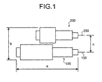
- Fig. 1 is a top view of an optical transmitter and an optical receiver used in an optical communication system according to an embodiment of the present invention.
- the optical communication system is based on the XFP standard.
- the length a of an optical transmitter 100 is 28 millimeters, the total breadth b of the optical transmitter 100 and the optical receiver 200 is 12 millimeters, and the distance c between optical axes of the optical transmitter 100 and the optical receiver 200 is 6 millimeters. These values satisfy the XFP standard.
- Fig. 2 is perspective view of an XFP standardized optical transmitter and receiver 300 that uses the optical transmitter and the optical receiver according to the embodiment.
- the XFP standardized optical transmitter and receiver 300 includes a case 301.
- the case 301 houses the optical transmitter 100 and the optical receiver 200.
- the case 301 includes an optical receiver insertion port 302 and an optical transmitter insertion port 303.
- the optical receiver 200 is inserted into the optical receiver insertion port 302, and the optical transmitter 100 is inserted into the optical transmitter insertion port 303.
- the width d of the case 301 is 18.35 ⁇ 0.1 millimeters.
- the distance e which is the between optical axes of the optical receiver insertion port 302 and the optical transmitter insertion port 303 is 6.0 millimeters.
- a board 304 is inserted into an extension slot or the like of a computer device that carries out optical communications at 10 Gigabits per second.
- a connector 306 and other circuitry are arranged on the board 304.
- the XFP standardized optical transmitter and receiver 300 can be connected to the connector 306 by inserting the XFP standardized optical transmitter and receiver 300 into an insertion port 305 provided to the board 304.
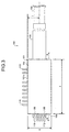
- Fig. 3 is an enlarged external view of the optical transmitter 100.
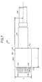
- Fig. 4 is an enlarged external view of the optical transmitter 100 from a different side.
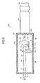
- Fig. 5 is a cross sectional view along the line A-A' shown in Fig. 3.
- Fig. 6 is a cross sectional view along the line B-B' shown in Fig. 4.
- the optical transmitter 100 includes a case 101.
- the case 101 is rectangular and hollow.
- the case includes an enclosure member 102 having a rectangular cross section (Refer to Fig. 6.), a lower member 103 that covers the lower surface of the enclosure member 102, and an upper member 104 that covers the upper surface of the enclosure member 102.
- This case 101 is made of a material having low heat conductivity, such as kovar.
- the lower member 103 is made of copper tungsten or the like having high heat conductivity.
- the case 101 houses a driver 108, a cooler 115, a laser generator 118, a first lens 123 and the like.
- an optical fiber tube 105 is jointed to the enclosure member 102.
- an optical fiber 150 is inserted and fixed thereto.
- a base 106 is of a roughly rectangular solid shape, and is arranged in the left half area in the figure of the lower member 103.
- This base 106 is made of copper tungsten and the like having a high heat conductivity.
- the left portion in the figure of the base 106 is formed to protrude outside.
- a high frequency board 107 is made of a ceramic material and the like such as alumina that has excellent high frequency properties, and is arranged onto the base 106.
- a roughly inverted u-shaped notched portion 107a, and a square hole 107b to meet the shape of a driver 108 are formed.
- the driver 108 has a function to drive and control a laser beam generator 118 to be described later herein, and is packaged onto the base 106 in a status contained in the square hole 107b. Meanwhile, heat generated in the driver 108 is spontaneously radiated via the base 106 and the lower member 103.
- wiring patterns are formed on the surface of the high frequency board 107.
- Relay terminals 109 are arranged on the base 106 at specified intervals, and part of each thereof protrudes outside from the enclosure member 102. These relay terminals 109 are connected via wires 111 to the respective wire patterns on the base 106.
- Terminals 112 are jointed to the relay terminals 109.
- Terminals 113 are arranged at specified intervals to protrude outside from the enclosure member 102, and are connected via wires 114 to the respective wiring patterns on the high frequency board 107.
- the cooler 115 shown in Fig. 5 is of roughly rectangular shape, and is arranged on the right of the base 106 in the lower member 103.
- This cooler 115 is a type that leads the heat generated in the laser beam generator 118, by use of the Peltier effect mentioned previously.
- This cooler 115 is made into a smaller size than that of the cooler used in the optical transmitter 10 mentioned previously (Refer to Fig. 11) through a contrivance to increase heat efficiency.
- the contrivance to increase heat efficiency is that a high heat conductivity member 116 is arranged onto the surface of the cooler 115, and further a low-heat-conductivity/high-weldability member 121 is arranged on the half portion of the high heat conductivity member 116, thereby heat efficiency (heat reduction) is increased in comparison with the conventional art.
- the high heat conductivity member 116 is made of a material (for example, copper tungsten) whose heat conductivity is higher than that of the conventional kovar (the material of the case 101), and is jointed onto the surface of the cooler 115.
- a support member 117 supports the laser beam generator 118.
- the support member 117 is made of a ceramic material or aluminum nitrogenous or the like.
- the support member 117 is jointed to the high heat conductivity member 116 by soldering or the like.
- This support member 117 is made of a material having high heat conductivity.
- the low-heat-conductivity/high-weldability member 121 is made of a material (for example, kovar) having heat conductivity lower than that of the high heat conductivity member 116, and having weldability by YAG welding higher than that of the high heat conductivity member 116.
- the low-heat-conductivity/high-weldability member 121 covers substantially half of the surface of the high heat conductivity member 116.
- This low-heat-conductivity/high-weldability member 121 has an area roughly half of that of the high heat conductivity member 116.
- the support member 117 is arranged in a position that is contained in the notched portion 107a (Refer to Fig. 6.).
- a support member 122 supports a first lens 123, and is made of SUS or kovar or the like. This support member 122 is jointed to the low-heat-conductivity/high-weldability member 121 by YAG welding. The low-heat-conductivity/high-weldability member 121 arranged between the support member 122 and the high heat conductivity material 116 allows firm fixing of the support member 122.
- the low-heat-conductivity/high-weldability member 121 functions as a heat barrier, and reduces the amount of heat, which is generated in the laser beam generator 118, conveyed toward the lens 123. Moreover, the low-heat-conductivity/high-weldability member 121 efficiency conveys the heat to the cooler 115.
- the laser beam generator 118 shown in Fig. 6 is positioned in the notched portion 107a and is arranged on the surface of the support member 117, and is driven and controlled by the driver 108. This laser generator 118 generates a laser beam toward the first lens 123.
- Wires 119 connect the wiring patterns formed on the high frequency board 107, and the wiring patterns formed on the surface of the support member 117. Accordingly, the driver 108 is electrically connected to the laser beam generator 118 via the wiring patterns of the high frequency board 107, wires 119 and the wiring patterns of the support member 117, and thereby drives and controls the laser beam generator 118.
- the first lens 123 is arranged in on the right of the laser beam generator 118, and converts the laser beam from the laser beam generator 118 into parallel light rays.
- a second lens 124 is arranged on the right of the first lens 123, and concentrates the parallel light rays from the first lens 123, and guides them to the incident surface of an optical fiber 150.
- a support member 125 is arranged in between the base 106 and the cooler 115, and is positioned in the notched portion 107a shown in Fig. 6.
- This support member 125 supports a measuring photo diode 126.
- the measuring photo diode 126 is a photo diode that measures the laser beam generated by the laser beam generator 118.
- a wire 127 connects the wiring patterns formed on the high frequency board 107, and the wiring patterns formed on the surface of the support member 125. Accordingly, the measuring photo diode 126 is electrically connected to the wiring patterns of the high frequency board 107 via the wiring patterns of the support member 125 and the wire 127.
- the laser beam generator 118 and the measuring photo diode 126 are arranged in the notched portion 107a, it becomes possible to make the size compact and still maintain high frequency properties.
- the optical transmitter 100 can be made smaller than the conventional optical transmitter 10 (Refer to Fig. 11.).
- the length direction size f is 13 millimeters
- the width direction size g is 6 millimeters
- the distance h from a side surface 101 a of the case 101 to the optical axis is 3 millimeters
- the height i is 6 millimeters.
- Fig. 7 is an enlarged external view of the optical receiver 200.
- Fig. 8 is an enlarged external view of the optical receiver 200 from a different direction.
- Fig. 9 is a cross sectional view along the line C-C' shown in Fig. 7.
- Fig. 10 is a cross sectional view along the line D-D' shown in Fig. 8.
- the optical receiver 200 includes a case 201.
- the case 201 is rectangular and hollow.
- the case 201 includes an enclosure member 202 of rectangular cross section (Refer to Fig. 10.), a lower member 203 that covers the lower surface of the enclosure member 202, and an upper member 204 that covers the upper surface of the enclosure member 202.
- This case 201 is made of a material having low heat conductivity, such as kovar.
- the case 201 houses a preamplifier 206, a photo diode 207 and the like.
- an optical fiber tube 205 is jointed to the enclosure member 202.
- an optical fiber 250 is inserted and fixed thereto.
- a base 217 is of a roughly rectangular shape, and is arranged in a portion that is on the right side in the lower member 203.
- a preamplifier 206 and a photo diode 207 are arranged to be detachable in unit of block. Therefore, in the optical receiver 200, the preamplifier 206 and the photo diode 207 may be exchanged in unit of block.
- a nonconforming block for example, the preamplifier 206
- a block to be changed for example, the photo diode 207
- the preamplifier 206 amplifies electric signals from the photo diodes 207.
- the photo diode 207 receives a laser beam that comes through the optical fiber 250, and converts the laser beam concerned into electric signals, and outputs the signals to the preamplifier 206.
- a wire 208 connects the preamplifier 206 and the photo diode 207.
- a lens 209 is arranged in the right area in the figure of the photo diode 207, and concentrates the laser beam that is ejected from the outgoing surface of the optical fiber 250, and leads the laser beam to the photo diode 207.
- a base 210 is arranged in the left area in the figure of the base 217.
- Relay terminals 211 are arranged on the base 210 at specified intervals.
- Wires 212 connect the relay terminals 211 and the respective terminals on the base 217.
- a base 213 is arranged in the left area in the figure of the base 210, and part thereof protrudes outside from the enclosure member 202 (Refer to Fig. 9.).
- Relay terminals 214 correspond to the relay terminals 211, and are arranged on the surface of the base 213 at specified intervals.
- Wires 215 connect the relay terminals 211 and the relay terminals 214.
- Terminals 216 are arranged at specified intervals to protrude outside from the enclosure member 202, and are connected to the relay terminals 214.
- the optical receiver 200 is made into a smaller size in comparison with the conventional optical receiver 20 (Refer to Fig. 11.).
- the length direction size j shown in Fig. 7 is 8 millimeters.
- the width direction size k is 6 millimeters.
- the distance I from a side surface 201 a of the case 201 to the optical axis is 3 millimeters.
- the height m shown in Fig. 8 is 6 millimeters.
- a laser beam is ejected from the laser beam generator 118.
- This laser beam is converted into parallel light rays by the first lens 123, which are concentrated by the second lens 124, and enter the incident surface of the optical fiber 150, and go through the optical fiber 150.
- heat generated in the laser beam generator 118 is conveyed to the cooler 115 via the support member 117 and the high heat conductivity member 116.
- the high heat conductivity member 116 is arranged on the entire surface of the cooler 115, and the heat barrier of the low-heat-conductivity/high-weldability member 121 is arranged, as a consequence, the heat generated in the laser beam generator 118 transfers to the cooler 115 at high efficiency.
- the laser beam that comes through the optical fiber 250 is ejected from the outgoing surface, and is concentrated by the lens 209, and converted into electric signals by the photo diode 207. Heat generated in the preamplifier 206 and the photo diode 207 is spontaneously radiated.
- the distance h from the side surface 101 a of the case 101 to the optical axis (Refer to Fig. 3.) is 3 millimeters
- the distance I from the side surface 201a of the case 201 to the optical axis (Refer to Fig. 7.) is 3 millimeters
- the distance c (Refer to Fig. 1.) becomes 6 millimeters, which conforms to the XFP standard explained previously.
- the width direction size k of the optical receiver 200 is 5 millimeters
- the distance I from the side surface 201 a of the case 201 to the optical axis is 2.5 millimeters.
- the width direction size g of the optical transmitter 100 may be expanded up to 7 millimeters, and the distance h from the side surface 101 a of the case 101 to the optical axis is made 3.5 millimeters.
- the distance c conforms to the XFP standard 6 millimeters (2.5 millimeters + 3.5 millimeters). It is preferred that the distance h (or l) from the side surface 101a (or the side surface 201a) of the case 101 (or the case 201) is made equal to or less than 3.5 millimeters, or in the range from 2.5 millimeters to 3.5 millimeters.
- the exemplary structure in which the low-heat-conductivity/high-weldability member 121 is arranged in between the high heat conductivity member 116 and the support member 122 shown in Fig. 5 has been explained, however, in the place of the low-heat-conductivity/high-weldability member 121, an adhesive that has a lower heat conductivity than that of the high heat conductivity member 116, and can physically join the high heat conductivity member 116 and the support member 122 firmly may be employed.
- the exemplary structure in which the low-heat-conductivity/high-weldability member 121 is arranged has been explained, however, when sufficient heat efficiency can be obtained, and the support member 122 can be firmly jointed to the high heat conductivity member 116, a structure may be made so that the support member 122 is jointed directly to the high heat conductivity member 116, without arranging the low-heat-conductivity/high-weldability member 121.
- the cooling method of the cooler 115 is the cooling method by Peltier effect, however, the present invention is not limited to this, but other cooling method may be employed.
- the optical transmitter 100 and the optical receiver 200 may be either a type with an optical fiber at delivery or a type without an optical fiber at delivery (receptacle).
- the first lens 123 shown in Fig. 5 on the cooler 115, but the first lens 123 (the support member 122) may be arranged in the right area in the figure from the cooler 115.
- the laser beam generator 118, the first lens 123, and the cooler 115 are arranged in the case 101, and the high heat conductivity member 116 that has a higher heat conductivity than that of the case 101, and leads heat generated in the laser beam generator 118 to the cooler 115 is arranged, therefore, it is possible to make the size of the cooler 115 small through high heat efficiency, and to obtain a compact size.
- the case 101 is made of kovar, and the high heat conductivity member 116 is made of copper tungsten, therefore, it is possible to make the size of the cooler 115 small through high heat efficiency, and to obtain a compact size.
- the low-heat-conductivity/high-weldability member 121 that is placed in between the high heat conductivity member 116 and the first lens 123, and has a higher heat conductivity than that of the high heat conductivity member 116 is arranged, therefore, it is possible to reduce the amount of the heat that is generated in the laser beam generator 118 and transfers to the lens 123 side, and to lead the heat to the cooler 115 at high efficiency.
- the support member 117 that supports the laser beam generator 118 and is jointed to the high heat conductivity member 116, and the support member 122 that supports the first lens 123 and is jointed to the low-heat-conductivity/high-weldability member 121 are arranged, consequently, the heat is led via the support member 117 to the cooler 115, therefore, it is possible to make the size of the cooler 115 small through high heat efficiency, and to obtain a compact size.
- the low-heat-conductivity/high-weldability member 121 that is placed in between the high heat conductivity member 116 and the support member 122, and has a lower heat conductivity than that of the high heat conductivity member 116 is arranged, therefore, it is possible to reduce the amount of the heat that is generated in the laser beam generator 118 and transfers to the lens 123 side, and to lead the heat to the cooler 115 at high efficiency.
- the high heat conductivity member 116 and the support member 122 are jointed with an adhesive that has a lower heat conductivity than that of the high heat conductivity member 116, therefore, it is possible to reduce the amount of the heat that is generated in the laser beam generator 118 and transfers to the lens 123 side, and to lead the heat to the cooler 115 at high efficiency.
- the low-heat-conductivity/high-weldability member 121 is made of kovar, therefore, it is possible to reduce the amount of the heat that is generated in the laser beam generator 118 and transfers to the lens 123 side, and to lead the heat to the cooler 115 at high efficiency.
- the high frequency board 107 in which the notched portion 107a for containing the laser beam generator 118 is formed, and the driver 108 that is placed on the high frequency board 107, and drives and controls the laser beam generator 118 are arranged, therefore, it is possible to make wires 119 shortest under the conditions for a compact size (for example, the width size g being 6 millimeters), and to maintain high frequency properties.
- the distance h from the side surface of the case 101 to the optical axis of the optical fiber 150 (Refer to Fig. 3.) is made equal to or less than 3.5 millimeters, therefore, it is possible to cope with the compact size of the optical transmitter 100 in a specified standard (for example, the XFP standard).
- the distance h from the side surface of the case 101 to the optical axis of the optical fiber 150 (Refer to Fig. 3.) is made 2.5 millimeters to 3.5 millimeters, therefore, it is possible to cope with the compact size of the optical transmitter 100 in a specified standard.
- the distance h from the side surface of the case 101 to the optical axis of the optical fiber 150 (Refer to Fig. 3.) is made 3 millimeters, therefore, it is possible to cope with the compact size of the optical transmitter 100 in a specified standard.
- the width direction size g of the case 101 (Refer to Fig. 3.) is made 6 millimeters, therefore, it is possible to cope with the compact size of the optical transmitter 100 in a specified standard.
- the photo diode 207 and the preamplifier 206 are arranged in the case 201, and the photo diode 207 and the preamplifier 206 are supported to be detachable in unit of block, therefore, it is possible to easily exchange a nonconforming block or a block to be exchanged, and to increase easy modifications in tests and designs.
- the cooler that cools down the heat generated in the photo diode 207 and the preamplifier 206 arranged in the case 201 is arranged, therefore, it is possible to use the photo diode 207 and the preamplifier 206 with a large amount of heat dissipation.
- the high heat conductivity member that is placed in between the photo diode 207 and the preamplifier 206, and has a higher heat conductivity than that of the case 201, and leads the heat generated in the photo diode 207 and the preamplifier 206 respectively to the cooler is arranged, therefore, it is possible to make the size of the cooler small through high heat efficiency, and to obtain a compact size.
- the case 201 is made of kovar, and the high heat conductivity member is made of copper tungsten, therefore, it is possible to make the size of the cooler small through high heat efficiency, and to obtain a compact size.
- the distance I from the side surface of the case 201 to the optical axis of the optical fiber 250 (Refer to Fig. 7.) is made equal to or less than 3.5 millimeters, therefore, it is possible to cope with the compact size of an optical receiver in a specified standard.
- the distance I from the side surface of the case 201 to the optical axis of the optical fiber 250 (Refer to Fig. 7.) is made 2.5 millimeters to 3.5 millimeters, therefore, it is possible to cope with the compact size of an optical receiver in a specified standard.
- the distance I from the side surface of the case 201 to the optical axis of the optical fiber 250 (Refer to Fig. 7.) is made 3 millimeters, therefore, it is possible to cope with the compact size of the optical receiver 200 in a specified standard.
- the width direction size k of the case 201 (Refer to Fig. 7.) is made 6 millimeters, therefore, it is possible to cope with the compact size of the optical receiver 200 in a specified standard.
- the XFP standardized optical transmitter and receiver 300 it is possible to obtain a compact size, to maintain high frequency properties, and to reduce exchange costs.
- a high heat conductivity member conveys the heat generated in the laser beam generating unit to the cooling unit, the heat can be conveyed efficiently.
- a small-sized cooling unit can be employed so that the overall size can be made compact.
- the low heat conductivity member that is placed in between the high heat conductivity member and the lens, and has a lower heat conductivity than that of the high heat conductivity member is arranged, therefore, there is an advantage that it is possible to reduce the amount of the heat that is generated in the laser beam generating unit and transfers to the lens side, and to lead the heat to the cooling unit at high efficiency.
- the first support member that supports the laser beam generating unit and is jointed to the high heat conductivity member, and the second support member that supports the lens and is jointed to the high heat conductivity member are arranged, consequently, the heat is led via the first support member to the cooling unit, therefore, there is an advantage that it is possible to make the size of the cooling unit small through high heat efficiency, and to obtain a compact size.
- the low heat conductivity member that is placed in between the high heat conductivity member and the second support member, and has a lower heat conductivity than that of the high heat conductivity member is arranged, therefore, there is an advantage that it is possible to reduce the amount of the heat that is generated in the laser beam generating unit and transfers to the lens side, and to lead the heat to the cooling unit at high efficiency.
- the high heat conductivity member and the second support member are jointed with an adhesive that has a lower heat conductivity than that of the high heat conductivity member, therefore, there is an advantage that it is possible to reduce the amount of the heat that is generated in the laser beam generating unit and transfers to the lens side, and to lead the heat to the cooling unit at high efficiency.
- the low heat conductivity member is made of kovar, therefore, there is an advantage that it is possible to reduce the amount of the heat that is generated in the laser beam generating unit and transfers to the lens side, and to lead the heat to the cooling unit at high efficiency.
- the board in which a notched portion for containing the laser beam generating unit is formed, and the driver that is arranged on the board, and drives and controls the laser beam generating unit are arranged, therefore, there is an advantage that it is possible to make lead wires shorter and achieve compact sizeain high frequency properties.
- the distance from the side surface of the case to the optical axis of the optical fiber is made equal to or less than 3.5 millimeters, therefore, there is an advantage that it is possible to cope with the compact size of an optical transmitter in a specified standard.
- the distance from the side surface of the case to the optical axis of the optical fiber is made 2.5 millimeters to 3.5 millimeters, therefore, there is an advantage that it is possible to cope with the compact size of an optical transmitter in a specified standard.
- the distance from the side surface of the case to the optical axis of the optical fiber is made 3 millimeters, therefore, there is an advantage that it is possible to cope with the compact size of an optical transmitter in a specified standard.
- the width direction size of the case is made 6 millimeters, therefore, there is an advantage that it is possible to cope with the compact size of an optical transmitter in a specified standard.
- the light receiving unit and the amplifying unit are arranged in the case, and the light receiving unit and the amplifying unit are supported to be detachable in unit of block, therefore, there is an advantage that it is possible to easily exchange a nonconforming block or a block to be exchanged, and to increase easy modifications in tests and designs.
- the cooling unit that cools down the heat generated in the light receiving unit and the amplifying unit arranged in the case is arranged, therefore, there is an advantage that it is possible to use a light receiving unit and an amplifying unit with a large amount of heat dissipation.
- the high heat conductivity member that is placed in between the light receiving unit and the amplifying unit, and has a higher heat conductivity than that of the case, and leads the heat generated in the light receiving unit and the amplifying unit respectively to the cooling unit is arranged, therefore, there is an advantage that it is possible to make the size of the cooling unit small through high heat efficiency, and to obtain a compact size.
- the case is made of kovar, and the high heat conductivity member is made of copper tungsten, therefore, there is an advantage that it is possible to make the size of the cooling unit small through high heat efficiency, and to obtain a compact size.
- the distance from the side surface of the case to the optical axis of the optical fiber is made equal to or less than 3.5 millimeters, therefore, there is an advantage that it is possible to cope with the compact size of an optical receiver in a specified standard.
- the distance from the side surface of the case to the optical axis of the optical fiber is made 2.5 millimeters to 3.5 millimeters, therefore, there is an advantage that it is possible to cope with the compact size of an optical receiver in a specified standard.
- the distance from the side surface of the case to the optical axis of the optical fiber is made 3 millimeters, therefore, there is an advantage that it is possible to cope with the compact size of an optical receiver in a specified standard.
- the width direction size of the case is made 6 millimeters, therefore, there is an advantage that it is possible to cope with the compact size of an optical receiver in a specified standard.
Landscapes
- Physics & Mathematics (AREA)
- General Physics & Mathematics (AREA)
- Optics & Photonics (AREA)
- Condensed Matter Physics & Semiconductors (AREA)
- Electromagnetism (AREA)
- Optical Couplings Of Light Guides (AREA)
- Light Receiving Elements (AREA)
- Semiconductor Lasers (AREA)
Priority Applications (1)
| Application Number | Priority Date | Filing Date | Title |
|---|---|---|---|
| EP05009047A EP1571714A3 (de) | 2003-10-31 | 2004-10-22 | Optischer Empfänger und optisches Kommunikationssystem |
Applications Claiming Priority (2)
| Application Number | Priority Date | Filing Date | Title |
|---|---|---|---|
| JP2003372730 | 2003-10-31 | ||
| JP2003372730A JP3977315B2 (ja) | 2003-10-31 | 2003-10-31 | 光通信器、光通信システムおよび光送受信器 |
Related Child Applications (1)
| Application Number | Title | Priority Date | Filing Date |
|---|---|---|---|
| EP05009047A Division EP1571714A3 (de) | 2003-10-31 | 2004-10-22 | Optischer Empfänger und optisches Kommunikationssystem |
Publications (2)
| Publication Number | Publication Date |
|---|---|
| EP1528417A2 true EP1528417A2 (de) | 2005-05-04 |
| EP1528417A3 EP1528417A3 (de) | 2005-08-24 |
Family
ID=34420242
Family Applications (2)
| Application Number | Title | Priority Date | Filing Date |
|---|---|---|---|
| EP04256552A Withdrawn EP1528417A3 (de) | 2003-10-31 | 2004-10-22 | Optischer Sender, optischer Empfänger, optisches Übertragungssystem, und optischer Sender/Empfänger |
| EP05009047A Withdrawn EP1571714A3 (de) | 2003-10-31 | 2004-10-22 | Optischer Empfänger und optisches Kommunikationssystem |
Family Applications After (1)
| Application Number | Title | Priority Date | Filing Date |
|---|---|---|---|
| EP05009047A Withdrawn EP1571714A3 (de) | 2003-10-31 | 2004-10-22 | Optischer Empfänger und optisches Kommunikationssystem |
Country Status (3)
| Country | Link |
|---|---|
| US (1) | US7561805B2 (de) |
| EP (2) | EP1528417A3 (de) |
| JP (1) | JP3977315B2 (de) |
Cited By (1)
| Publication number | Priority date | Publication date | Assignee | Title |
|---|---|---|---|---|
| GB2477740A (en) * | 2010-02-10 | 2011-08-17 | Oclaro Technology Plc | Reduced length optoelectronic device |
Families Citing this family (10)
| Publication number | Priority date | Publication date | Assignee | Title |
|---|---|---|---|---|
| WO2007123140A1 (ja) * | 2006-04-20 | 2007-11-01 | Nec Corporation | 通信装置及び通信装置の空冷方法 |
| JP4914775B2 (ja) * | 2007-06-11 | 2012-04-11 | ファイベスト株式会社 | 光モジュール |
| JP2010093747A (ja) * | 2008-10-10 | 2010-04-22 | Sony Corp | 固体撮像素子及び信号処理システム |
| EP2859391B1 (de) | 2012-04-19 | 2022-11-30 | OE Solutions America Inc. | Kühlungssystem für vorrichtungen und baugruppen |
| US9614619B1 (en) * | 2014-10-10 | 2017-04-04 | Google Inc. | Optical transceiver having separate transmitter and receiver lenses |
| US9641254B1 (en) | 2014-10-10 | 2017-05-02 | Google Inc. | Heat dissipation approach in chip on board assembly by using stacked copper microvias |
| US10901161B2 (en) | 2018-09-14 | 2021-01-26 | Toyota Motor Engineering & Manufacturing North America, Inc. | Optical power transfer devices with an embedded active cooling chip |
| US10707964B2 (en) * | 2018-10-03 | 2020-07-07 | Prime World International Holdings Ltd. | Optical transceiver and housing thereof |
| JP7370160B2 (ja) * | 2019-04-12 | 2023-10-27 | 日本ルメンタム株式会社 | 光伝送装置 |
| TWI757808B (zh) * | 2020-07-31 | 2022-03-11 | 華星光通科技股份有限公司 | 具多通道散熱結構之光發射器 |
Citations (1)
| Publication number | Priority date | Publication date | Assignee | Title |
|---|---|---|---|---|
| EP0911923A2 (de) | 1997-10-24 | 1999-04-28 | Nec Corporation | Halbleiterlaserbauelement |
Family Cites Families (29)
| Publication number | Priority date | Publication date | Assignee | Title |
|---|---|---|---|---|
| JPH03120884A (ja) | 1989-10-04 | 1991-05-23 | Hitachi Ltd | 半導体レーザモジュール |
| JPH08179170A (ja) | 1994-12-27 | 1996-07-12 | Hitachi Ltd | 熱電子冷却素子付半導体レーザモジュール |
| JPH10190141A (ja) * | 1996-12-20 | 1998-07-21 | Fujitsu Ltd | 光半導体モジュール |
| US6027256A (en) | 1997-02-07 | 2000-02-22 | Coherent, Inc. | Composite laser diode enclosure and method for making the same |
| JPH10223962A (ja) * | 1997-02-12 | 1998-08-21 | Furukawa Electric Co Ltd:The | 光ファイバアンプ用複合モジュール |
| US6155724A (en) * | 1997-03-04 | 2000-12-05 | Hamamatsu Photonics Kk | Light transmitting module for optical communication and light transmitting unit thereof |
| JPH11248973A (ja) | 1998-02-27 | 1999-09-17 | Ntt Electornics Corp | 光モジュール |
| JP2000277843A (ja) | 1999-03-23 | 2000-10-06 | Nec Corp | 半導体レーザモジュールとその製造方法 |
| US6609838B1 (en) * | 2000-01-20 | 2003-08-26 | Jds Uniphase Corporation | Removable small form factor fiber optic transceiver module chassis |
| JP2002082261A (ja) | 2000-07-07 | 2002-03-22 | Hitachi Cable Ltd | 光送信器、光受信器及び光送受信器 |
| US6677570B1 (en) * | 2000-09-22 | 2004-01-13 | Nortel Networks Limited | Wide dynamic range optical power detector |
| EP1215782A3 (de) * | 2000-12-15 | 2004-01-07 | The Furukawa Electric Co., Ltd. | Integriertes Modul für Synthese von Laserstrahlen für einen Halbleiterlasermodul und optischen Verstärker |
| JP2002261265A (ja) * | 2001-03-06 | 2002-09-13 | Sumitomo Electric Ind Ltd | 光通信装置 |
| US6826916B2 (en) * | 2001-04-24 | 2004-12-07 | The Furukawa Electric Co., Ltd. | Laser module, Peltier module, and Peltier module integrated heat spreader |
| EP1284530A3 (de) * | 2001-06-26 | 2003-11-26 | The Furukawa Electric Co., Ltd. | Optisches Modul |
| US6603093B2 (en) * | 2001-08-08 | 2003-08-05 | Intel Corporation | Method for alignment of optical components using laser welding |
| KR100413848B1 (ko) | 2001-09-15 | 2004-01-03 | 주식회사 래피더스 | 광모듈용 밀폐형 패키지 |
| US6623180B2 (en) * | 2001-10-19 | 2003-09-23 | Gtran, Inc. | High frequency optical module and method of making same |
| JP4001744B2 (ja) * | 2001-12-27 | 2007-10-31 | 三菱電機株式会社 | 受光素子キャリアおよび光受信装置 |
| JP2003215406A (ja) | 2002-01-21 | 2003-07-30 | Kyocera Corp | 半導体レーザモジュールとその製造方法 |
| US7215886B2 (en) * | 2002-02-04 | 2007-05-08 | Hitachi, Ltd. | Optical communication module |
| JP4015440B2 (ja) | 2002-02-26 | 2007-11-28 | 日本オプネクスト株式会社 | 光通信モジュール |
| US20050138934A1 (en) | 2002-02-14 | 2005-06-30 | Martin Weigert | Optoelectronic component with a peltier cooler |
| US6653557B2 (en) * | 2002-02-27 | 2003-11-25 | Jds Uniphase Corporation | Faraday cage and ceramic walls for shielding EMI |
| US6647039B2 (en) * | 2002-02-27 | 2003-11-11 | Jds Uniphase Corporation | Reconfigurable laser header |
| JP2003264331A (ja) | 2002-03-11 | 2003-09-19 | Opnext Japan Inc | 光モジュール |
| JP2003309312A (ja) * | 2002-04-15 | 2003-10-31 | Opnext Japan Inc | 光モジュール |
| US7120178B2 (en) * | 2002-06-15 | 2006-10-10 | Intel Corporation | Chip carrier apparatus and method |
| JP3982362B2 (ja) * | 2002-08-23 | 2007-09-26 | 住友電気工業株式会社 | 光データリンク |
-
2003
- 2003-10-31 JP JP2003372730A patent/JP3977315B2/ja not_active Expired - Fee Related
-
2004
- 2004-10-20 US US10/970,695 patent/US7561805B2/en not_active Expired - Lifetime
- 2004-10-22 EP EP04256552A patent/EP1528417A3/de not_active Withdrawn
- 2004-10-22 EP EP05009047A patent/EP1571714A3/de not_active Withdrawn
Patent Citations (1)
| Publication number | Priority date | Publication date | Assignee | Title |
|---|---|---|---|---|
| EP0911923A2 (de) | 1997-10-24 | 1999-04-28 | Nec Corporation | Halbleiterlaserbauelement |
Cited By (3)
| Publication number | Priority date | Publication date | Assignee | Title |
|---|---|---|---|---|
| GB2477740A (en) * | 2010-02-10 | 2011-08-17 | Oclaro Technology Plc | Reduced length optoelectronic device |
| GB2477740B (en) * | 2010-02-10 | 2014-06-25 | Oclaro Technology Ltd | Reduced length optoelectronic devices |
| US9488784B2 (en) | 2010-02-10 | 2016-11-08 | Oclaro Technology Limited | Reduced length optoelectronic devices |
Also Published As
| Publication number | Publication date |
|---|---|
| US7561805B2 (en) | 2009-07-14 |
| JP3977315B2 (ja) | 2007-09-19 |
| EP1571714A3 (de) | 2005-11-30 |
| EP1571714A2 (de) | 2005-09-07 |
| EP1528417A3 (de) | 2005-08-24 |
| US20050094686A1 (en) | 2005-05-05 |
| JP2005136327A (ja) | 2005-05-26 |
Similar Documents
| Publication | Publication Date | Title |
|---|---|---|
| US20030206703A1 (en) | Transmitters, receivers, and transceivers including an optical bench | |
| KR100615898B1 (ko) | 합파 레이저광원 및 노광장치 | |
| US5127072A (en) | Laser module with compliant optical fiber coupling | |
| JP2003142766A (ja) | 組込み式温度制御部付きコンパクトレーザーパッケージ | |
| US10656355B2 (en) | Heat dissipation structure of horizontal optical-communication sub-assembly | |
| EP1528417A2 (de) | Optischer Sender, optischer Empfänger, optisches Übertragungssystem, und optischer Sender/Empfänger | |
| US6736553B1 (en) | VCSEL array optical subassembly module with alignment mechanism | |
| JP2005167189A (ja) | 光−電気変換モジュール及びそれを用いた光トランシーバ | |
| KR100627701B1 (ko) | 병렬 광접속 모듈 | |
| JP2010122312A (ja) | 送受信レンズブロック及びそれを用いた光モジュール | |
| US20030128552A1 (en) | Light generating module | |
| US20180278014A1 (en) | Optical subassembly, optical module, and optical transmission equipment | |
| US20040091268A1 (en) | Transmitter optical sub-assembly | |
| JP2010122311A (ja) | レンズブロック及びそれを用いた光モジュール | |
| JP2009025458A (ja) | 光モジュール | |
| CN100470971C (zh) | 光学模块 | |
| JP2005292739A (ja) | 光モジュール | |
| US5123067A (en) | Optical head capable of being fitted into a hybrid circuit | |
| JP2004085756A (ja) | 光送受信モジュール | |
| JP2003241028A (ja) | 光送信モジュール | |
| JPS60221713A (ja) | 光電モジユ−ルケ−シング | |
| JP2005159036A (ja) | 光送受信モジュール | |
| JPH05175608A (ja) | 光半導体素子モジュール | |
| CN111258008A (zh) | 具有垂直地安装的监控光二极管的光发射次组件配置 | |
| JP2022037163A (ja) | 光サブアセンブリ、光モジュール、及び光伝送装置 |
Legal Events
| Date | Code | Title | Description |
|---|---|---|---|
| PUAI | Public reference made under article 153(3) epc to a published international application that has entered the european phase |
Free format text: ORIGINAL CODE: 0009012 |
|
| 17P | Request for examination filed |
Effective date: 20050105 |
|
| AK | Designated contracting states |
Kind code of ref document: A2 Designated state(s): AT BE BG CH CY CZ DE DK EE ES FI FR GB GR HU IE IT LI LU MC NL PL PT RO SE SI SK TR |
|
| AX | Request for extension of the european patent |
Extension state: AL HR LT LV MK |
|
| PUAL | Search report despatched |
Free format text: ORIGINAL CODE: 0009013 |
|
| AK | Designated contracting states |
Kind code of ref document: A3 Designated state(s): AT BE BG CH CY CZ DE DK EE ES FI FR GB GR HU IE IT LI LU MC NL PL PT RO SE SI SK TR |
|
| AX | Request for extension of the european patent |
Extension state: AL HR LT LV MK |
|
| AKX | Designation fees paid |
Designated state(s): DE FR GB IT |
|
| 17Q | First examination report despatched |
Effective date: 20060928 |
|
| RAP1 | Party data changed (applicant data changed or rights of an application transferred) |
Owner name: MACOM TECHNOLOGY SOLUTIONS HOLDINGS, INC. |
|
| GRAP | Despatch of communication of intention to grant a patent |
Free format text: ORIGINAL CODE: EPIDOSNIGR1 |
|
| STAA | Information on the status of an ep patent application or granted ep patent |
Free format text: STATUS: GRANT OF PATENT IS INTENDED |
|
| INTG | Intention to grant announced |
Effective date: 20190723 |
|
| RIN1 | Information on inventor provided before grant (corrected) |
Inventor name: NOTOMI, SEISHI Inventor name: AOKI, HIROATSU |
|
| STAA | Information on the status of an ep patent application or granted ep patent |
Free format text: STATUS: THE APPLICATION IS DEEMED TO BE WITHDRAWN |
|
| 18D | Application deemed to be withdrawn |
Effective date: 20191203 |