EP1521328B1 - Solar cell - Google Patents
Solar cell Download PDFInfo
- Publication number
- EP1521328B1 EP1521328B1 EP03762895A EP03762895A EP1521328B1 EP 1521328 B1 EP1521328 B1 EP 1521328B1 EP 03762895 A EP03762895 A EP 03762895A EP 03762895 A EP03762895 A EP 03762895A EP 1521328 B1 EP1521328 B1 EP 1521328B1
- Authority
- EP
- European Patent Office
- Prior art keywords
- solar cell
- electrolyte solution
- cell
- ions
- semiconductor
- Prior art date
- Legal status (The legal status is an assumption and is not a legal conclusion. Google has not performed a legal analysis and makes no representation as to the accuracy of the status listed.)
- Expired - Lifetime
Links
- 239000008151 electrolyte solution Substances 0.000 claims description 41
- 239000004065 semiconductor Substances 0.000 claims description 36
- 229910052709 silver Inorganic materials 0.000 claims description 23
- 239000004332 silver Substances 0.000 claims description 23
- -1 silver ions Chemical class 0.000 claims description 20
- 229910021645 metal ion Inorganic materials 0.000 claims description 19
- 238000010248 power generation Methods 0.000 claims description 16
- ZCYVEMRRCGMTRW-UHFFFAOYSA-N 7553-56-2 Chemical compound [I] ZCYVEMRRCGMTRW-UHFFFAOYSA-N 0.000 claims description 15
- 229910052740 iodine Inorganic materials 0.000 claims description 15
- 239000011630 iodine Substances 0.000 claims description 15
- BQCADISMDOOEFD-UHFFFAOYSA-N Silver Chemical compound [Ag] BQCADISMDOOEFD-UHFFFAOYSA-N 0.000 claims description 13
- 239000003792 electrolyte Substances 0.000 claims description 9
- 238000006479 redox reaction Methods 0.000 claims description 5
- 239000010410 layer Substances 0.000 description 24
- 238000000034 method Methods 0.000 description 23
- 239000000975 dye Substances 0.000 description 22
- WEVYAHXRMPXWCK-UHFFFAOYSA-N Acetonitrile Chemical compound CC#N WEVYAHXRMPXWCK-UHFFFAOYSA-N 0.000 description 12
- 230000007423 decrease Effects 0.000 description 11
- 239000000758 substrate Substances 0.000 description 10
- 239000003990 capacitor Substances 0.000 description 9
- 230000005611 electricity Effects 0.000 description 9
- 239000000243 solution Substances 0.000 description 9
- BASFCYQUMIYNBI-UHFFFAOYSA-N platinum Chemical compound [Pt] BASFCYQUMIYNBI-UHFFFAOYSA-N 0.000 description 8
- 238000006243 chemical reaction Methods 0.000 description 7
- 230000006870 function Effects 0.000 description 7
- 229910052751 metal Inorganic materials 0.000 description 7
- 239000002184 metal Substances 0.000 description 7
- 239000002904 solvent Substances 0.000 description 7
- 150000002500 ions Chemical class 0.000 description 6
- 230000008859 change Effects 0.000 description 5
- 230000000052 comparative effect Effects 0.000 description 5
- 229910044991 metal oxide Inorganic materials 0.000 description 5
- 150000004706 metal oxides Chemical class 0.000 description 5
- PXHVJJICTQNCMI-UHFFFAOYSA-N Nickel Chemical compound [Ni] PXHVJJICTQNCMI-UHFFFAOYSA-N 0.000 description 4
- GWEVSGVZZGPLCZ-UHFFFAOYSA-N Titan oxide Chemical compound O=[Ti]=O GWEVSGVZZGPLCZ-UHFFFAOYSA-N 0.000 description 4
- 238000010586 diagram Methods 0.000 description 4
- 239000011521 glass Substances 0.000 description 4
- HSZCZNFXUDYRKD-UHFFFAOYSA-M lithium iodide Chemical compound [Li+].[I-] HSZCZNFXUDYRKD-UHFFFAOYSA-M 0.000 description 4
- 229910052697 platinum Inorganic materials 0.000 description 4
- 229920006395 saturated elastomer Polymers 0.000 description 4
- 229910052782 aluminium Inorganic materials 0.000 description 3
- 239000002131 composite material Substances 0.000 description 3
- 239000004020 conductor Substances 0.000 description 3
- 239000000463 material Substances 0.000 description 3
- SZTSOGYCXBVMMT-UHFFFAOYSA-N 2,4-dimethyl-1-propylimidazole;hydroiodide Chemical compound [I-].CCC[NH+]1C=C(C)N=C1C SZTSOGYCXBVMMT-UHFFFAOYSA-N 0.000 description 2
- YEJRWHAVMIAJKC-UHFFFAOYSA-N 4-Butyrolactone Chemical compound O=C1CCCO1 YEJRWHAVMIAJKC-UHFFFAOYSA-N 0.000 description 2
- RYGMFSIKBFXOCR-UHFFFAOYSA-N Copper Chemical compound [Cu] RYGMFSIKBFXOCR-UHFFFAOYSA-N 0.000 description 2
- LFQSCWFLJHTTHZ-UHFFFAOYSA-N Ethanol Chemical compound CCO LFQSCWFLJHTTHZ-UHFFFAOYSA-N 0.000 description 2
- HBBGRARXTFLTSG-UHFFFAOYSA-N Lithium ion Chemical compound [Li+] HBBGRARXTFLTSG-UHFFFAOYSA-N 0.000 description 2
- 239000012327 Ruthenium complex Substances 0.000 description 2
- DKGAVHZHDRPRBM-UHFFFAOYSA-N Tert-Butanol Chemical compound CC(C)(C)O DKGAVHZHDRPRBM-UHFFFAOYSA-N 0.000 description 2
- XLOMVQKBTHCTTD-UHFFFAOYSA-N Zinc monoxide Chemical compound [Zn]=O XLOMVQKBTHCTTD-UHFFFAOYSA-N 0.000 description 2
- XAGFODPZIPBFFR-UHFFFAOYSA-N aluminium Chemical compound [Al] XAGFODPZIPBFFR-UHFFFAOYSA-N 0.000 description 2
- 150000001768 cations Chemical class 0.000 description 2
- 238000000576 coating method Methods 0.000 description 2
- 229910001429 cobalt ion Inorganic materials 0.000 description 2
- XLJKHNWPARRRJB-UHFFFAOYSA-N cobalt(2+) Chemical compound [Co+2] XLJKHNWPARRRJB-UHFFFAOYSA-N 0.000 description 2
- 238000007796 conventional method Methods 0.000 description 2
- 229910052802 copper Inorganic materials 0.000 description 2
- 239000010949 copper Substances 0.000 description 2
- 230000003247 decreasing effect Effects 0.000 description 2
- 238000000151 deposition Methods 0.000 description 2
- 230000008021 deposition Effects 0.000 description 2
- 238000010828 elution Methods 0.000 description 2
- PCHJSUWPFVWCPO-UHFFFAOYSA-N gold Chemical compound [Au] PCHJSUWPFVWCPO-UHFFFAOYSA-N 0.000 description 2
- 229910052737 gold Inorganic materials 0.000 description 2
- 239000010931 gold Substances 0.000 description 2
- 229910003437 indium oxide Inorganic materials 0.000 description 2
- PJXISJQVUVHSOJ-UHFFFAOYSA-N indium(iii) oxide Chemical compound [O-2].[O-2].[O-2].[In+3].[In+3] PJXISJQVUVHSOJ-UHFFFAOYSA-N 0.000 description 2
- MRELNEQAGSRDBK-UHFFFAOYSA-N lanthanum(3+);oxygen(2-) Chemical compound [O-2].[O-2].[O-2].[La+3].[La+3] MRELNEQAGSRDBK-UHFFFAOYSA-N 0.000 description 2
- 239000007788 liquid Substances 0.000 description 2
- 229910001416 lithium ion Inorganic materials 0.000 description 2
- 239000000434 metal complex dye Substances 0.000 description 2
- 230000005012 migration Effects 0.000 description 2
- 238000013508 migration Methods 0.000 description 2
- 239000000203 mixture Substances 0.000 description 2
- PLDDOISOJJCEMH-UHFFFAOYSA-N neodymium(3+);oxygen(2-) Chemical compound [O-2].[O-2].[O-2].[Nd+3].[Nd+3] PLDDOISOJJCEMH-UHFFFAOYSA-N 0.000 description 2
- 229910052759 nickel Inorganic materials 0.000 description 2
- 239000011255 nonaqueous electrolyte Substances 0.000 description 2
- 239000002245 particle Substances 0.000 description 2
- IEQIEDJGQAUEQZ-UHFFFAOYSA-N phthalocyanine Chemical compound N1C(N=C2C3=CC=CC=C3C(N=C3C4=CC=CC=C4C(=N4)N3)=N2)=C(C=CC=C2)C2=C1N=C1C2=CC=CC=C2C4=N1 IEQIEDJGQAUEQZ-UHFFFAOYSA-N 0.000 description 2
- 238000005240 physical vapour deposition Methods 0.000 description 2
- 150000004032 porphyrins Chemical class 0.000 description 2
- 239000000843 powder Substances 0.000 description 2
- 238000001556 precipitation Methods 0.000 description 2
- 230000008569 process Effects 0.000 description 2
- 239000011241 protective layer Substances 0.000 description 2
- 238000004544 sputter deposition Methods 0.000 description 2
- IATRAKWUXMZMIY-UHFFFAOYSA-N strontium oxide Chemical compound [O-2].[Sr+2] IATRAKWUXMZMIY-UHFFFAOYSA-N 0.000 description 2
- XOLBLPGZBRYERU-UHFFFAOYSA-N tin dioxide Chemical compound O=[Sn]=O XOLBLPGZBRYERU-UHFFFAOYSA-N 0.000 description 2
- 229910001887 tin oxide Inorganic materials 0.000 description 2
- OGIDPMRJRNCKJF-UHFFFAOYSA-N titanium oxide Inorganic materials [Ti]=O OGIDPMRJRNCKJF-UHFFFAOYSA-N 0.000 description 2
- UINDRJHZBAGQFD-UHFFFAOYSA-O 2-ethyl-3-methyl-1h-imidazol-3-ium Chemical compound CCC1=[NH+]C=CN1C UINDRJHZBAGQFD-UHFFFAOYSA-O 0.000 description 1
- QKPVEISEHYYHRH-UHFFFAOYSA-N 2-methoxyacetonitrile Chemical compound COCC#N QKPVEISEHYYHRH-UHFFFAOYSA-N 0.000 description 1
- CPELXLSAUQHCOX-UHFFFAOYSA-M Bromide Chemical compound [Br-] CPELXLSAUQHCOX-UHFFFAOYSA-M 0.000 description 1
- WKBOTKDWSSQWDR-UHFFFAOYSA-N Bromine atom Chemical compound [Br] WKBOTKDWSSQWDR-UHFFFAOYSA-N 0.000 description 1
- XMWRBQBLMFGWIX-UHFFFAOYSA-N C60 fullerene Chemical class C12=C3C(C4=C56)=C7C8=C5C5=C9C%10=C6C6=C4C1=C1C4=C6C6=C%10C%10=C9C9=C%11C5=C8C5=C8C7=C3C3=C7C2=C1C1=C2C4=C6C4=C%10C6=C9C9=C%11C5=C5C8=C3C3=C7C1=C1C2=C4C6=C2C9=C5C3=C12 XMWRBQBLMFGWIX-UHFFFAOYSA-N 0.000 description 1
- OKTJSMMVPCPJKN-UHFFFAOYSA-N Carbon Chemical compound [C] OKTJSMMVPCPJKN-UHFFFAOYSA-N 0.000 description 1
- JPVYNHNXODAKFH-UHFFFAOYSA-N Cu2+ Chemical compound [Cu+2] JPVYNHNXODAKFH-UHFFFAOYSA-N 0.000 description 1
- PQMOXTJVIYEOQL-UHFFFAOYSA-N Cumarin Natural products CC(C)=CCC1=C(O)C(C(=O)C(C)CC)=C(O)C2=C1OC(=O)C=C2CCC PQMOXTJVIYEOQL-UHFFFAOYSA-N 0.000 description 1
- KMTRUDSVKNLOMY-UHFFFAOYSA-N Ethylene carbonate Chemical compound O=C1OCCO1 KMTRUDSVKNLOMY-UHFFFAOYSA-N 0.000 description 1
- FYYHWMGAXLPEAU-UHFFFAOYSA-N Magnesium Chemical compound [Mg] FYYHWMGAXLPEAU-UHFFFAOYSA-N 0.000 description 1
- FSOGIJPGPZWNGO-UHFFFAOYSA-N Meomammein Natural products CCC(C)C(=O)C1=C(O)C(CC=C(C)C)=C(O)C2=C1OC(=O)C=C2CCC FSOGIJPGPZWNGO-UHFFFAOYSA-N 0.000 description 1
- 229930182559 Natural dye Natural products 0.000 description 1
- VEQPNABPJHWNSG-UHFFFAOYSA-N Nickel(2+) Chemical compound [Ni+2] VEQPNABPJHWNSG-UHFFFAOYSA-N 0.000 description 1
- 206010070834 Sensitisation Diseases 0.000 description 1
- GSEJCLTVZPLZKY-UHFFFAOYSA-N Triethanolamine Chemical compound OCCN(CCO)CCO GSEJCLTVZPLZKY-UHFFFAOYSA-N 0.000 description 1
- MCMNRKCIXSYSNV-UHFFFAOYSA-N ZrO2 Inorganic materials O=[Zr]=O MCMNRKCIXSYSNV-UHFFFAOYSA-N 0.000 description 1
- XHCLAFWTIXFWPH-UHFFFAOYSA-N [O-2].[O-2].[O-2].[O-2].[O-2].[V+5].[V+5] Chemical compound [O-2].[O-2].[O-2].[O-2].[O-2].[V+5].[V+5] XHCLAFWTIXFWPH-UHFFFAOYSA-N 0.000 description 1
- 238000010521 absorption reaction Methods 0.000 description 1
- 239000000987 azo dye Substances 0.000 description 1
- 239000011324 bead Substances 0.000 description 1
- 230000006399 behavior Effects 0.000 description 1
- 238000005452 bending Methods 0.000 description 1
- GDTBXPJZTBHREO-UHFFFAOYSA-N bromine Substances BrBr GDTBXPJZTBHREO-UHFFFAOYSA-N 0.000 description 1
- 229910052794 bromium Inorganic materials 0.000 description 1
- 229910052793 cadmium Inorganic materials 0.000 description 1
- BDOSMKKIYDKNTQ-UHFFFAOYSA-N cadmium atom Chemical compound [Cd] BDOSMKKIYDKNTQ-UHFFFAOYSA-N 0.000 description 1
- WLZRMCYVCSSEQC-UHFFFAOYSA-N cadmium(2+) Chemical compound [Cd+2] WLZRMCYVCSSEQC-UHFFFAOYSA-N 0.000 description 1
- 229910052799 carbon Inorganic materials 0.000 description 1
- 239000000919 ceramic Substances 0.000 description 1
- 229910000420 cerium oxide Inorganic materials 0.000 description 1
- 238000005229 chemical vapour deposition Methods 0.000 description 1
- 239000011248 coating agent Substances 0.000 description 1
- 229910017052 cobalt Inorganic materials 0.000 description 1
- 239000010941 cobalt Substances 0.000 description 1
- GUTLYIVDDKVIGB-UHFFFAOYSA-N cobalt atom Chemical compound [Co] GUTLYIVDDKVIGB-UHFFFAOYSA-N 0.000 description 1
- 150000001875 compounds Chemical class 0.000 description 1
- 230000006835 compression Effects 0.000 description 1
- 238000007906 compression Methods 0.000 description 1
- 229910001431 copper ion Inorganic materials 0.000 description 1
- ZYGHJZDHTFUPRJ-UHFFFAOYSA-N coumarin Chemical compound C1=CC=C2OC(=O)C=CC2=C1 ZYGHJZDHTFUPRJ-UHFFFAOYSA-N 0.000 description 1
- 230000001419 dependent effect Effects 0.000 description 1
- 238000007598 dipping method Methods 0.000 description 1
- 238000007606 doctor blade method Methods 0.000 description 1
- 238000004070 electrodeposition Methods 0.000 description 1
- SEACYXSIPDVVMV-UHFFFAOYSA-L eosin Y Chemical compound [Na+].[Na+].[O-]C(=O)C1=CC=CC=C1C1=C2C=C(Br)C(=O)C(Br)=C2OC2=C(Br)C([O-])=C(Br)C=C21 SEACYXSIPDVVMV-UHFFFAOYSA-L 0.000 description 1
- 238000011156 evaluation Methods 0.000 description 1
- 230000005284 excitation Effects 0.000 description 1
- 230000001747 exhibiting effect Effects 0.000 description 1
- 238000001125 extrusion Methods 0.000 description 1
- 239000010419 fine particle Substances 0.000 description 1
- 239000004088 foaming agent Substances 0.000 description 1
- 239000011245 gel electrolyte Substances 0.000 description 1
- 229910000449 hafnium oxide Inorganic materials 0.000 description 1
- WIHZLLGSGQNAGK-UHFFFAOYSA-N hafnium(4+);oxygen(2-) Chemical compound [O-2].[O-2].[Hf+4] WIHZLLGSGQNAGK-UHFFFAOYSA-N 0.000 description 1
- 239000012943 hotmelt Substances 0.000 description 1
- XMBWDFGMSWQBCA-UHFFFAOYSA-N hydrogen iodide Chemical compound I XMBWDFGMSWQBCA-UHFFFAOYSA-N 0.000 description 1
- 229910052738 indium Inorganic materials 0.000 description 1
- APFVFJFRJDLVQX-UHFFFAOYSA-N indium atom Chemical compound [In] APFVFJFRJDLVQX-UHFFFAOYSA-N 0.000 description 1
- 239000011810 insulating material Substances 0.000 description 1
- XMBWDFGMSWQBCA-UHFFFAOYSA-M iodide Chemical compound [I-] XMBWDFGMSWQBCA-UHFFFAOYSA-M 0.000 description 1
- 238000007733 ion plating Methods 0.000 description 1
- 230000001678 irradiating effect Effects 0.000 description 1
- 239000011244 liquid electrolyte Substances 0.000 description 1
- 229910052749 magnesium Inorganic materials 0.000 description 1
- 239000011777 magnesium Substances 0.000 description 1
- 238000004519 manufacturing process Methods 0.000 description 1
- DZVCFNFOPIZQKX-LTHRDKTGSA-M merocyanine Chemical compound [Na+].O=C1N(CCCC)C(=O)N(CCCC)C(=O)C1=C\C=C\C=C/1N(CCCS([O-])(=O)=O)C2=CC=CC=C2O\1 DZVCFNFOPIZQKX-LTHRDKTGSA-M 0.000 description 1
- 150000002739 metals Chemical class 0.000 description 1
- 125000001434 methanylylidene group Chemical group [H]C#[*] 0.000 description 1
- CQDGTJPVBWZJAZ-UHFFFAOYSA-N monoethyl carbonate Chemical compound CCOC(O)=O CQDGTJPVBWZJAZ-UHFFFAOYSA-N 0.000 description 1
- 239000002105 nanoparticle Substances 0.000 description 1
- 239000000978 natural dye Substances 0.000 description 1
- 229910001453 nickel ion Inorganic materials 0.000 description 1
- 229910000484 niobium oxide Inorganic materials 0.000 description 1
- URLJKFSTXLNXLG-UHFFFAOYSA-N niobium(5+);oxygen(2-) Chemical compound [O-2].[O-2].[O-2].[O-2].[O-2].[Nb+5].[Nb+5] URLJKFSTXLNXLG-UHFFFAOYSA-N 0.000 description 1
- QGLKJKCYBOYXKC-UHFFFAOYSA-N nonaoxidotritungsten Chemical compound O=[W]1(=O)O[W](=O)(=O)O[W](=O)(=O)O1 QGLKJKCYBOYXKC-UHFFFAOYSA-N 0.000 description 1
- 238000007254 oxidation reaction Methods 0.000 description 1
- BMMGVYCKOGBVEV-UHFFFAOYSA-N oxo(oxoceriooxy)cerium Chemical compound [Ce]=O.O=[Ce]=O BMMGVYCKOGBVEV-UHFFFAOYSA-N 0.000 description 1
- SIWVEOZUMHYXCS-UHFFFAOYSA-N oxo(oxoyttriooxy)yttrium Chemical compound O=[Y]O[Y]=O SIWVEOZUMHYXCS-UHFFFAOYSA-N 0.000 description 1
- BPUBBGLMJRNUCC-UHFFFAOYSA-N oxygen(2-);tantalum(5+) Chemical compound [O-2].[O-2].[O-2].[O-2].[O-2].[Ta+5].[Ta+5] BPUBBGLMJRNUCC-UHFFFAOYSA-N 0.000 description 1
- RVTZCBVAJQQJTK-UHFFFAOYSA-N oxygen(2-);zirconium(4+) Chemical compound [O-2].[O-2].[Zr+4] RVTZCBVAJQQJTK-UHFFFAOYSA-N 0.000 description 1
- 238000007747 plating Methods 0.000 description 1
- 229920000642 polymer Polymers 0.000 description 1
- 238000002360 preparation method Methods 0.000 description 1
- FVSKHRXBFJPNKK-UHFFFAOYSA-N propionitrile Chemical compound CCC#N FVSKHRXBFJPNKK-UHFFFAOYSA-N 0.000 description 1
- FOWDZVNRQHPXDO-UHFFFAOYSA-N propyl hydrogen carbonate Chemical compound CCCOC(O)=O FOWDZVNRQHPXDO-UHFFFAOYSA-N 0.000 description 1
- RUOJZAUFBMNUDX-UHFFFAOYSA-N propylene carbonate Chemical compound CC1COC(=O)O1 RUOJZAUFBMNUDX-UHFFFAOYSA-N 0.000 description 1
- WCYJXDMUQGVQQS-UHFFFAOYSA-N pyridine;ruthenium Chemical compound [Ru].C1=CC=NC=C1 WCYJXDMUQGVQQS-UHFFFAOYSA-N 0.000 description 1
- 150000004053 quinones Chemical class 0.000 description 1
- 230000005855 radiation Effects 0.000 description 1
- 230000009467 reduction Effects 0.000 description 1
- 238000006722 reduction reaction Methods 0.000 description 1
- 239000011347 resin Substances 0.000 description 1
- 229920005989 resin Polymers 0.000 description 1
- PYWVYCXTNDRMGF-UHFFFAOYSA-N rhodamine B Chemical compound [Cl-].C=12C=CC(=[N+](CC)CC)C=C2OC2=CC(N(CC)CC)=CC=C2C=1C1=CC=CC=C1C(O)=O PYWVYCXTNDRMGF-UHFFFAOYSA-N 0.000 description 1
- 150000003839 salts Chemical class 0.000 description 1
- 238000007650 screen-printing Methods 0.000 description 1
- 238000007789 sealing Methods 0.000 description 1
- 230000008313 sensitization Effects 0.000 description 1
- 230000001235 sensitizing effect Effects 0.000 description 1
- 239000002356 single layer Substances 0.000 description 1
- 238000005245 sintering Methods 0.000 description 1
- 238000002791 soaking Methods 0.000 description 1
- 238000003980 solgel method Methods 0.000 description 1
- 239000007784 solid electrolyte Substances 0.000 description 1
- 238000004528 spin coating Methods 0.000 description 1
- 239000007921 spray Substances 0.000 description 1
- 239000003115 supporting electrolyte Substances 0.000 description 1
- 229910001936 tantalum oxide Inorganic materials 0.000 description 1
- 238000002207 thermal evaporation Methods 0.000 description 1
- 229910001930 tungsten oxide Inorganic materials 0.000 description 1
- 229910001935 vanadium oxide Inorganic materials 0.000 description 1
- 239000011787 zinc oxide Substances 0.000 description 1
Images

Classifications
-
- H—ELECTRICITY
- H01—ELECTRIC ELEMENTS
- H01M—PROCESSES OR MEANS, e.g. BATTERIES, FOR THE DIRECT CONVERSION OF CHEMICAL ENERGY INTO ELECTRICAL ENERGY
- H01M14/00—Electrochemical current or voltage generators not provided for in groups H01M6/00 - H01M12/00; Manufacture thereof
- H01M14/005—Photoelectrochemical storage cells
-
- H—ELECTRICITY
- H01—ELECTRIC ELEMENTS
- H01M—PROCESSES OR MEANS, e.g. BATTERIES, FOR THE DIRECT CONVERSION OF CHEMICAL ENERGY INTO ELECTRICAL ENERGY
- H01M14/00—Electrochemical current or voltage generators not provided for in groups H01M6/00 - H01M12/00; Manufacture thereof
-
- H—ELECTRICITY
- H01—ELECTRIC ELEMENTS
- H01G—CAPACITORS; CAPACITORS, RECTIFIERS, DETECTORS, SWITCHING DEVICES OR LIGHT-SENSITIVE DEVICES, OF THE ELECTROLYTIC TYPE
- H01G9/00—Electrolytic capacitors, rectifiers, detectors, switching devices, light-sensitive or temperature-sensitive devices; Processes of their manufacture
- H01G9/20—Light-sensitive devices
- H01G9/2004—Light-sensitive devices characterised by the electrolyte, e.g. comprising an organic electrolyte
-
- H—ELECTRICITY
- H01—ELECTRIC ELEMENTS
- H01G—CAPACITORS; CAPACITORS, RECTIFIERS, DETECTORS, SWITCHING DEVICES OR LIGHT-SENSITIVE DEVICES, OF THE ELECTROLYTIC TYPE
- H01G9/00—Electrolytic capacitors, rectifiers, detectors, switching devices, light-sensitive or temperature-sensitive devices; Processes of their manufacture
- H01G9/20—Light-sensitive devices
- H01G9/2027—Light-sensitive devices comprising an oxide semiconductor electrode
- H01G9/2031—Light-sensitive devices comprising an oxide semiconductor electrode comprising titanium oxide, e.g. TiO2
-
- H—ELECTRICITY
- H01—ELECTRIC ELEMENTS
- H01L—SEMICONDUCTOR DEVICES NOT COVERED BY CLASS H10
- H01L31/00—Semiconductor devices sensitive to infrared radiation, light, electromagnetic radiation of shorter wavelength or corpuscular radiation and specially adapted either for the conversion of the energy of such radiation into electrical energy or for the control of electrical energy by such radiation; Processes or apparatus specially adapted for the manufacture or treatment thereof or of parts thereof; Details thereof
- H01L31/04—Semiconductor devices sensitive to infrared radiation, light, electromagnetic radiation of shorter wavelength or corpuscular radiation and specially adapted either for the conversion of the energy of such radiation into electrical energy or for the control of electrical energy by such radiation; Processes or apparatus specially adapted for the manufacture or treatment thereof or of parts thereof; Details thereof adapted as photovoltaic [PV] conversion devices
-
- Y—GENERAL TAGGING OF NEW TECHNOLOGICAL DEVELOPMENTS; GENERAL TAGGING OF CROSS-SECTIONAL TECHNOLOGIES SPANNING OVER SEVERAL SECTIONS OF THE IPC; TECHNICAL SUBJECTS COVERED BY FORMER USPC CROSS-REFERENCE ART COLLECTIONS [XRACs] AND DIGESTS
- Y02—TECHNOLOGIES OR APPLICATIONS FOR MITIGATION OR ADAPTATION AGAINST CLIMATE CHANGE
- Y02E—REDUCTION OF GREENHOUSE GAS [GHG] EMISSIONS, RELATED TO ENERGY GENERATION, TRANSMISSION OR DISTRIBUTION
- Y02E10/00—Energy generation through renewable energy sources
- Y02E10/50—Photovoltaic [PV] energy
- Y02E10/542—Dye sensitized solar cells
Definitions
- the invention relates to a photovoltaic power generation apparatus.
- the solar cell when light is converted to electricity in a solar cell, such as a dye sensitization solar cell, the solar cell generates electricity having a current that is proportional to the amount of incident light and a constant voltage that is dependent on the internal electric potential difference.
- the voltage varies in proportion to the amount of incident light due to recoupling of electric charges and the like. For example, as the amount of incident light decreases, the voltage decreases as well as the current.
- a stable supply of electrical power is crucial.
- the current-voltage output from the solar cell which varies in proportion to the amount of incident light should be converted to a stable current-voltage characteristic.
- a stabilized power supply circuit 1 such as a switching power supply, is provided.
- the output from the solar cell main body 2 can be stabilized by providing the output from the solar cell main body 2 to the stabilized power supply circuit 1; thus, a stable electrical power can be supplied to an external apparatus.
- the stabilized power supply circuit 1 To drive the stabilized power supply circuit 1, a certain electrical power must be supplied thereto. For this reason, the current-voltage output from the solar cell main body 2 should fall within a certain range. If sunlight is temporarily blocked, for example by clouds, the output power from the solar cell main body 2 will decrease temporarily, and the stabilized power supply circuit 1 will stop functioning since the electrical power required to drive the stabilized power supply circuit 1 is no longer supplied. As a result, a stable supply of electrical power will be no longer available.
- One method to overcome this shortcoming is to install in the solar cell a secondary cell or a large-capacity capacitor which has a voltage characteristic comparable to the generation voltage of the solar cell.
- this method when a large amount of light incident on the solar cell and an electrical power with a voltage higher than a predetermined voltage is generated, the secondary cell or the capacitor is charged whereas the secondary cell or the capacitor discharges when the amount of incident light is low and an electrical power with a voltage lower than the predetermined voltage is generated.
- this method it is possible to reduce the incidence of stopping of the stabilized power supply circuit 1.
- addition of such a device external to a solar cell may cause an increase in power loss caused by resistance and the like, and a solar cell can only supply a power as low as a value lower than the actual power generation capacity of the solar cell.
- addition of an external device may increase the price of the solar cell since the structure of a solar cell and a power generation apparatus using a solar cell may become complex. This method is not a viable option when a low-cost photovoltaic power generation apparatus is desired.
- Solar cells are used in a photovoltaic power generation apparatus in which multiple solar cell panels having a predetermined size are arranged. Although solar cell panels connected in parallel pose no problem, in a solar cell in which panels are connected in series for the purpose of reducing power loss caused by resistance or increasing an open-circuit voltage (output voltage), the output power of the apparatus as a whole will significantly decrease because not much current flows in those panels when light incident on some of the panels is blocked by clouds or obstacles.
- JP 09 306553 A discloses a photoelectric conversion secondary cell in which a composite semiconductor layer to which dye are absorbed is inserted between a transparent conductor which is formed on a surface of a transparent supporting medium and a counter electrode, a redox solution in which an oxidized species is colored and a reduced species is colorless is filed between the transparent conductor and the composite semiconductor layer, and a metallic species is filed between the counter electrode and the composite semiconductor layer.
- MAHESHWAR SHARON ET AL " SOLAR RECHARGEABLE BATTERY-PRINCIPLE AND MATERIALS*"ELECTROCHIMICA ACTA, ELSEVIER SCIENCE PUBLISHERS, BARKING, GB LNKD-DOI:10.1016/0013-4686 (91)85097-Q, vol. 36, no. 7, 1 January 1991 (1991-01-01), pages 1107-1126, XP000226178ISSN: 0013-4686 , discloses a solar cell comprising a semiconductor, a counter electrode, and an electrolyte solution (page 1115, Fig. 11).
- the electrolyte solution comprises silver ions, which may be reduced at the backside of the semiconductor electrode. They also may be dissolved from the semiconductor electrode. Therefore, the solar cell also works as a secondary cell.
- JP 10 208782 A describes a solar cell which can store electrical energy.
- the electrolyte of the cell comprises lithium ions taking part in a reduction/oxidation reaction.
- the invention is based on a photovoltaic power generation apparatus as per the preamble of claim 1. It is the objective of the invention to provide a photovoltaic power generation apparatus providing a stable electrical power.
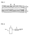
- FIG. 1 is a schematic cross-sectional view of a liquid junction solar cell, as an example of the solar cell according to a first embodiment of the present invention.
- a transparent conductive layer 12 is provided on one side of a transparent substrate 11.
- a transparent substrate 11 glass, or plastic, or the like, may be used.
- conductive metal oxide such as tin-doped indium oxide (ITO), fluorine-doped tin oxide (FTO), or the like, may be used.
- the transparent substrate 11 is not necessarily required, provided that a transparent conductive layer 12 that is sufficiently strong and provides a sufficient sealing performance is used.
- current collecting wirings 13 made of metal films, such as gold, platinum, silver, copper, aluminum, nickel, cadmium, or the like, are provided.
- the current collecting wirings 13 are disposed spaced apart from each other so that light can pass through between the current collecting wirings 13.
- any conventional method such as plating, physical vapor deposition (PVD; sputtering, ion plating, or the like), chemical vapor deposition (CVD; thermal deposition, plasma deposition, radiation deposition, or the like), spin coating, squeegee method, doctor blade method, screen printing, or the like, may be used.
- the resultant film may be patterned according to requirement to form the grid- or mesh-like current collecting wirings 13.
- a semiconductor layer 14 is provided as a protective layer of the wirings 13. Electric charges generated in the semiconductor layer 14 are collected by the current collecting wirings 13, and are pumped to the transparent electrically conductive film 12.
- any semiconducting material may be used, and a metal oxide or the like is preferably used.
- a metal oxide include titanium oxide, tin oxide, tungsten oxide, zinc oxide, zirconium dioxide, neodymium oxide, hafnium oxide, strontium oxide, indium oxide, cerium oxide, yttrium oxide, lanthanum oxide, vanadium oxide, niobium oxide, tantalum oxide, and the like.
- the semiconductor layer 14 is preferably a porous film.
- the porous film may be formed using a conventional method, such as a sol-gel method, migration electro-deposition of fine particles, a method using a foaming agent, coating with a mixture of polymer beads or the like followed by removal of the extra component, sintering method, or the like.
- a method in which semiconductor particles are sintered to form a porous sintered body is particularly preferable.
- porous semiconductor material may be subjected to a treatment to increase the surface area thereof.
- the sintered body may be loaded with dye on its surface.
- the dye any compounds that have an absorption band in the visible light range or near infrared range and exhibit an excitation behavior suitable for the semiconductor may be used.
- the dye examples include organic dyes, such as azo dyes, methine dye, fullerene derivatives, quinones, cumarin, eosine, rhodamine, merocyanine, or the like; metal complex dyes such as porphyrin, phthalocyanine, or the like; or ruthenium complex dyes; natural dyes such as those derived from plants, or the like.
- Preferable dyes are metal complex dyes, such as phthalocyanine, porphyrin or the like, or ruthenium complex dyes.
- a solar cell on which a dye is loaded is referred to as a dye-sensitized solar cell.
- a method for sensitizing with a dye is to dip a staked body of the transparent substrate 11, the transparent conductive layer 12, and the semiconductor layer 13 into a solution containing a dye, and then to dry or heat-dry the stacked body at room temperature to sensitize the semiconductor layer 13 with the dye.
- the present invention is not limited to this technique, and other methods including soaking methods, such as dipping methods, roller method, air knife method, or the like; coating methods, such as wire bar method, slide hopper method, extrusion method, curtain method, spin method, spray method, or the like, may be used.
- the transparent substrate 11, the transparent electrically conductive film 12, and the current collecting wirings 13, and the semiconductor layer 14 are stacked together to form a working electrode 15.
- a counter electrode 16 includes a substrate 17 and a conductive layer 18, and is a conductive substrate in which the conductive layer 18 is provided on the substrate 17.
- the substrate 17 is made of an insulating material, such as glass, ceramic, or the like.
- metals platinum, gold, silver, copper, aluminum, magnesium, indium, or the like
- carbon conductive metal oxide (ITO, FTO), or the like
- ITO, FTO conductive metal oxide
- platinum, ITO, and FTO are preferable.
- the counter electrode 16 may have a single-layer structure of a conductive layer made of a conductive material.
- the working electrode 15 and the counter electrode 16 described above are arranged so that they oppose each other, and the electrolyte solution 19 is filled between the two electrodes to form a single cell.
- the cell has flexibility, it is possible to use the cell while bending it or to use the cell in an environment in which it is repeatedly bent.
- the electrolyte solution 19 may be either a nonaqueous electrolyte solution prepared by dissolving an electrolyte into a nonaqueous solvent, or a fused salt obtained by fusing an electrolyte.
- a nonaqueous electrolyte solution is used.
- the electrolyte (supporting electrolyte) lithium ions, cobalt ions, tetraalkyl ions, imidazolium ions may be used, for example.
- the nonaqueous solvent is required to have properties to dissolve the electrolyte and to dissociate it into ions, and nonaqueous solvents having a relative dielectric constant ⁇ r of greater than 20 is preferable.
- nonaqueous solvent examples include, but are not limited to, ethanol, acetonitrile, methoxy acetonitrile, propionitrile, ethyl carbonate, propyl carbonate, ethylene carbonate, propylene carbonate, ⁇ -butyrolactone, ethylmethyl imidazolium, and any solvent that is conventionally used as a solvent for preparing an electrolyte solution for a solar cell.
- These nonaqueous solvents are selected according to desired properties, or they may be used in combination.
- the electrolyte solution 19 contains a redox couple.
- the redox couple include, but not limited to, iodine/iodine ion, bromine/bromine ion, and cobalt/cobalt ion pairs.
- the dye-sensitized solar cell when light is incident on the semiconductor layer 14 of the working electrode 15, the dye absorbs the light to emit electrons.
- the emitted electrons migrate to the semiconductor layer 14 and travel to the working electrode 15.
- the reduced ions are again oxidized on the dye. This process is repeated, and electric current flows to generate electricity.
- metal ions such as silver ions, copper ions, cadmium ions, aluminum ions, nickel ions, or the like, are dissolved in the electrolyte solution 19. These metal ions are selected according to desired properties, and they may be used in combination. The metal ions are dissolved into the electrolyte solution 19 until they are saturated. It may be possible to dissolve particles of an elemental metal in the electrolyte solution 19. However, in the case in which the current collecting wirings 13 made of metal films are provided as in the case of this example, metal ions spontaneously elute from the current collecting wirings 13 to the electrolyte solution 19 may be used as the metal ions.
- the current collecting wirings 13 Since the metal in the current collecting wirings 13 elutes to the electrolyte solution 19 until it is saturated, the current collecting wirings 13 should be provided, considering the amount of metal eluted to the electrolyte solution 19, and the sufficient thickness of the current collecting wirings 13 so that the wirings 13 function as a collector.
- an oxidation-reduction reaction of the metal ions will occur, in addition to the above-described oxidation-reduction reaction of the redox couple.
- the oxidation-reduction reaction of the metal ions proceeds in the same electrolyte solution as the solar cell, which functions as another cell in the solar cell. In other words, the solar cell itself functions as a secondary cell.
- the oxidation-reduction reaction of the metal ions defines a secondary cell, the electric potential of which is slightly lower than the electromotive force of the solar cell.
- the solubility to the electrolyte solution 19 the balance between elution and precipitation of the metal ions when reaching saturation (equilibrium), and the capability to retain the voltage, or the like, may be considered.
- silver ions are preferably used as the metal ions since silver ions satisfy all of the following qualities: a high solubility, the balance between elution and precipitation when the solution reaches a state of equilibrium, and the capability to retain the voltage.
- the metal ions should not hinder the migration of other electrolyte ions in the electrolyte solution 19 in the solar cell.
- the charge voltage of the above-described secondary cell is slightly lower than the generation voltage of the solar cell in this example.
- the solar cell is charged when sufficient light is incident on the solar cell and the charge voltage of the above-described secondary cell that is higher than the generation voltage is generated.
- the secondary cell discharges.
- the electrolyte solution 19 has a brown color of triiodide ions. Since triiodide ions are reduced to iodide ions when light is incident, the electrolyte solution 19 turns to a colorless solution of iodide ions.
- silver and triiodide ions react to convert to silver ions and iodide ions as described above formulae (1) to (3), the electrolyte solution is maintained as a colorless solution.
- the cell therefore, may be tinted according to requirement.
- an electrolyte solution bath containing the electrolyte solution 19 and the metal ions may be provided outside of the solar cell.
- the charge capacity of the secondary cell can be enhanced and the open-circuit voltage can be obtained for a longer period of time when light is blocked or the amount of the light is small.
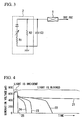
- FIG. 2 is a diagram illustrating an electric circuit of the above-described solar cell which is equipped with the ability to also function as a secondary cell, and the portion surrounded by the dotted line except for the secondary cells C1 and C2 is an equivalent circuit of the solar cell 2.
- R1 is the internal resistance
- R2 is the dielectric resistance. The part of the generated current flows in the dielectric resistance R2, which will be wasted as the leak current.
- the output from the solar cell is sent to the stabilized power supply circuit 1 as mentioned above.
- the secondary cells C1 and C2 are secondary cells functioning in this solar cell.
- the secondary cells C1 and C2 are charged by the generation voltage of the solar cell and discharge when the generation voltage of the solar cell drops.
- the electricity circuit shown in FIG. 3 is an electricity circuit of a solar cell in which a secondary cell or capacitor C3 is provided outside of the conventional solar cell 2.
- a secondary cell or capacitor C3 is provided outside of the conventional solar cell 2.
- the secondary cells C1 and C2 formed in the solar cell are charged without being influenced by the dielectric resistance R2.
- R2 the dielectric resistance
- An external secondary cell or capacitor may be provided to the solar cell. Since this solar cell includes an internal secondary cell internally, a small external secondary cell having a small capacity may be sufficient; thus it can be provided at a low cost. When the amount of incident light is low and the open-circuit voltage from the intrinsic solar cell is low, this external secondary cell or capacitor can be used to charge the internal secondary cell. Thus, efficiency of the utility of sunlight is further enhanced.
- the electrolyte solution of the present invention is not limited to a liquid electrolyte solution, and may be a solid electrolyte solution, such as a gel electrolyte solution.
- ion dissociative liquids such as triethanolamine, may be used.
- materials exhibiting opto-electric conversion characteristics such as an organic porous film, an inorganic porous film, or the like, may be used, in addition to a porous film of metal oxide.
- the photovoltaic power generation apparatus of the present invention includes one or more panels, and each of the panels has multiple solar cells mentioned above. When two or more panels are used, these solar cell panels may be connected in parallel or in series.
- recesses 30 may be provided to the counter electrode 16 of the solar cell in a longitudinal direction in the counter electrode 16 of the solar cell in order to facilitate the flow of the electrolyte solution 19, as shown in FIG. 5 .
- An electrolyte solution was obtained by dissolving 0.1 M of lithium iodide, 0.3 M of dimethylpropylimidazolium iodide, and 0.05 M of iodide were dissolved in acetonitrile, with respect to the entire electrolyte solution.
- 1.34% by weight of lithium iodide, 8.0% by weight of dimethylpropylimidazolium iodide, and 1.26% by weight of iodine were dissolved into 89.4% by weight of acetonitrile.
- a dye solution was obtained by dissolving 0.3 M of ruthenium pyridine complex into a mixture of 50% by weight of acetonitrile and 50% by weight of tert- butanol.
- a transparent electrically conductive film made of FTO was formed on a transparent glass substrate with a size of ten centimeters square, and mesh-like current collecting wirings having 90% of an open area ratio were formed on the transparent electrically conductive film using a sintered-type silver paste.
- a porous semiconductor film made of titanium oxide was formed as a protective layer of the wirings on the current collecting wirings
- titania nanoparticle paste was coated on the porous semiconductor film and sintered.
- the porous semiconductor film was dipped into a dye solution to sensitize the porous semiconductor film with the dye, and the porous semiconductor film was dried at room temperature to form a dye sensitized porous semiconductor film.
- the dye sensitized porous semiconductor film was used as a working electrode.
- a counter electrode was made by forming a staked body having a conductive film which is formed by sputtering platinum on a glass plate.
- the working electrode and the counter electrode were staked together, and they were adhered by hot melt resin or the like, or they were bonded by compression. Between the electrodes, an iodine-based electrolyte solution was filled and sealed to obtain a cell.
- the iodine-based electrolyte solution filled into the cell was changed from brown to colorless in about an hour because I 3 - ions were converted to I - ions, which confirmed that silver was dissolved from the current collecting wirings made of silver into the iodine-based electrolyte solution as silver ions.
- a cell was fabricated in a manner similar to that of Example 1, except that an iodine-based electrolyte was prepared by dissolving silver powders until they were saturated, and the current collecting wirings were not formed on the transparent electrically conductive film.
- a cell was fabricated in a manner similar to that of Example 1, except that an iodine-based electrolyte was prepared by dissolving nickel powders until they were saturated, and the current collecting wirings were not formed on the transparent electrically conductive film.
- a cell was fabricated in a manner similar to that of Example 1, except that the current collecting wirings were not formed on the transparent electrically conductive film.
- the cells of Examples 1 and 2 exhibited an excellent open-circuit voltage performance, which were comparable to the cell of the Comparative Example, which did not contain silver in the electrolyte solution. This confirms that the opto-electric conversion efficiency of a cell will not deteriorate if a large amount of silver is contained in the electrolyte solution.
- Curve 21 represents the change in the cell voltage of the cell in Example 1 with no-load (open) across the output terminals
- Curves 22 to 24 represent the change in the cell voltage when the current flowing across the terminals was increased when the resistances r2 to r4 across the output terminals of the cell in Example 1 were set to r2 > r3 > r4, and r2 was100 ⁇ , r3 was 10 ⁇ , r4 was 1 ⁇ .
- Curve 25 represents the change in the cell voltage of Comparative Example.
- Open-circuit voltages were almost the same for all of the cells as shown by Curves 21 to 25. It was confirmed that the open-circuit voltage dropped sharply by more than 50 to 100 mV when the light was blocked in Curves 21 to 24. After that, an open electrical power of about 500 mV was maintained in Curve 21 in which no current flowed whereas current decreased with in an increase in the current in Curves 22 to 24. As for Curve 25, the open-circuit voltage dropped sharply, and the open-circuit voltage was not maintained after light was blocked.
- the open-circuit voltage of the cell of Example 1 was evaluated in the similar manner by irradiating a light having an intensity of 100 W/m 2 using a solar simulator, and almost the same results were obtained, although the result is not shown in FIG. 4 .
- the solar cell of the present invention is equipped with a capability of being able to function as a secondary cell.
- the open-circuit voltage solar cell when used as a secondary cell is about 500 mV, which is a photoelectric property comparable to that of when light is incident. Furthermore, it was confirmed that the solar cell can be charged with a low amount of incident light, and that an electrical power of about 500 mV can be obtained, irrespective of the intensity of light.
- the solar cell of the present invention is equipped with a capability of being able to function as a secondary cell, the internal second cell discharges and the fluctuation of the output is reduced even when the amount of light incident on the solar cell is temporarily decreased and the output from the intrinsic solar cell drops; thus the output is stabilized.
- the secondary cell can be used to charge the internal secondary cell.
- efficiency of the utility of sunlight is enhanced compared to a conventional solar cell which is equipped with an external secondary cell or capacitor.
- the photovoltaic power generation apparatus of the present invention includes the solar cell described above, the stability of output and efficiency of the utility of sunlight is enhanced. Thus, it is possible to simplify accompanying electricity circuit or the like, and to provide the apparatus at a lower cost.
Applications Claiming Priority (3)
| Application Number | Priority Date | Filing Date | Title |
|---|---|---|---|
| JP2002199958 | 2002-07-09 | ||
| JP2002199958 | 2002-07-09 | ||
| PCT/JP2003/008653 WO2004006381A1 (ja) | 2002-07-09 | 2003-07-08 | 太陽電池 |
Publications (3)
| Publication Number | Publication Date |
|---|---|
| EP1521328A1 EP1521328A1 (en) | 2005-04-06 |
| EP1521328A4 EP1521328A4 (en) | 2010-05-12 |
| EP1521328B1 true EP1521328B1 (en) | 2013-03-06 |
Family
ID=30112495
Family Applications (1)
| Application Number | Title | Priority Date | Filing Date |
|---|---|---|---|
| EP03762895A Expired - Lifetime EP1521328B1 (en) | 2002-07-09 | 2003-07-08 | Solar cell |
Country Status (7)
| Country | Link |
|---|---|
| EP (1) | EP1521328B1 (ko) |
| JP (1) | JP4081084B2 (ko) |
| KR (1) | KR100681499B1 (ko) |
| CN (1) | CN1300894C (ko) |
| AU (1) | AU2003252477B2 (ko) |
| TW (2) | TW200703673A (ko) |
| WO (1) | WO2004006381A1 (ko) |
Families Citing this family (16)
| Publication number | Priority date | Publication date | Assignee | Title |
|---|---|---|---|---|
| JP4757433B2 (ja) * | 2003-03-24 | 2011-08-24 | 独立行政法人科学技術振興機構 | 太陽電池 |
| JP2005251736A (ja) * | 2004-02-02 | 2005-09-15 | Hitachi Maxell Ltd | 光電変換素子およびそれを用いた光電池、ならびに電子機器の筐体 |
| DE102004015769A1 (de) * | 2004-03-31 | 2005-11-03 | Fraunhofer-Gesellschaft zur Förderung der angewandten Forschung e.V. | Photoelektrochemisches Solarzellenmodul |
| JP2005353850A (ja) * | 2004-06-10 | 2005-12-22 | Ngk Spark Plug Co Ltd | 太陽電池用基板及び融雪機能付き太陽電池 |
| JP2006147261A (ja) * | 2004-11-17 | 2006-06-08 | Enplas Corp | 色素増感太陽電池の対向電極及び色素増感太陽電池 |
| JP4892197B2 (ja) * | 2005-04-01 | 2012-03-07 | 関西パイプ工業株式会社 | 色素増感型太陽電池用電極基板、色素増感型太陽電池用光電極および対向電極、ならびに色素増感型太陽電池 |
| TW200828607A (en) | 2006-12-11 | 2008-07-01 | Fujikura Ltd | Photoelectric conversion element |
| JP2009016174A (ja) * | 2007-07-04 | 2009-01-22 | Fujikura Ltd | 光電変換素子 |
| KR100997843B1 (ko) * | 2008-08-29 | 2010-12-01 | 주식회사 솔켐 | 전기방사법에 의해 제조된 고분자 전해질을 포함한 염료감응형 태양전지 소자 및 이의 제조방법 |
| KR101264111B1 (ko) * | 2010-06-04 | 2013-05-14 | 주식회사 나노신소재 | 투명도전막, 투명도전막용 타겟 및 투명도전막용 타겟의 제조방법 |
| JP5837405B2 (ja) * | 2011-11-28 | 2015-12-24 | 独立行政法人国立高等専門学校機構 | 光電変換素子及びその製造方法 |
| CN102610873A (zh) * | 2012-04-16 | 2012-07-25 | 常州大学 | 多孔纳米硅化学电池及其制备方法 |
| JP2013222661A (ja) * | 2012-04-18 | 2013-10-28 | Toshiba Corp | 光発電システムおよび蓄電装置 |
| JP5802819B1 (ja) * | 2014-11-12 | 2015-11-04 | 株式会社フジクラ | 低照度用色素増感光電変換素子の電解質、及び、これを用いた低照度用色素増感光電変換素子 |
| US9742194B2 (en) * | 2015-05-08 | 2017-08-22 | Solantro Semiconductor Corp. | Photovoltaic power system inverter detection |
| EP3151289A1 (en) * | 2015-10-01 | 2017-04-05 | LG Electronics Inc. | Solar cell |
Family Cites Families (10)
| Publication number | Priority date | Publication date | Assignee | Title |
|---|---|---|---|---|
| JP3025798B2 (ja) * | 1990-11-06 | 2000-03-27 | 日本電信電話株式会社 | 光化学2次電池及び光化学2次電池の製造方法 |
| JPH06215807A (ja) * | 1993-01-14 | 1994-08-05 | Nippon Telegr & Teleph Corp <Ntt> | 光2次電池 |
| JP3301454B2 (ja) * | 1993-10-28 | 2002-07-15 | 日本電信電話株式会社 | 光化学2次電池 |
| JP3304006B2 (ja) * | 1993-11-01 | 2002-07-22 | 日本電信電話株式会社 | 光化学2次電池 |
| JPH07245125A (ja) * | 1994-03-04 | 1995-09-19 | Miyazaki Univ | 発電可能な二次電池 |
| JPH09306553A (ja) * | 1996-05-08 | 1997-11-28 | Kagaku Gijutsu Shinko Jigyodan | 光電変換型二次電池 |
| JP3448444B2 (ja) * | 1997-01-29 | 2003-09-22 | 三洋電機株式会社 | 光蓄電池 |
| US6479745B2 (en) * | 2000-01-26 | 2002-11-12 | Sharp Kabushiki Kaisha | Dye-sensitized solar cell and method of manufacturing the same |
| TWI234885B (en) * | 2002-03-26 | 2005-06-21 | Fujikura Ltd | Electroconductive glass and photovoltaic cell using the same |
| WO2004032274A1 (ja) * | 2002-10-03 | 2004-04-15 | Fujikura Ltd. | 電極基板、光電変換素子、導電性ガラス基板およびその製造方法、並びに色素増感太陽電池 |
-
2003
- 2003-07-08 TW TW095125686A patent/TW200703673A/zh unknown
- 2003-07-08 JP JP2004519294A patent/JP4081084B2/ja not_active Expired - Fee Related
- 2003-07-08 AU AU2003252477A patent/AU2003252477B2/en not_active Ceased
- 2003-07-08 WO PCT/JP2003/008653 patent/WO2004006381A1/ja active IP Right Grant
- 2003-07-08 CN CNB038159732A patent/CN1300894C/zh not_active Expired - Fee Related
- 2003-07-08 KR KR1020047021645A patent/KR100681499B1/ko not_active IP Right Cessation
- 2003-07-08 EP EP03762895A patent/EP1521328B1/en not_active Expired - Lifetime
- 2003-07-08 TW TW092118596A patent/TWI314785B/zh not_active IP Right Cessation
Also Published As
| Publication number | Publication date |
|---|---|
| JP4081084B2 (ja) | 2008-04-23 |
| TWI314785B (en) | 2009-09-11 |
| WO2004006381A1 (ja) | 2004-01-15 |
| TW200402893A (en) | 2004-02-16 |
| KR20050029134A (ko) | 2005-03-24 |
| EP1521328A1 (en) | 2005-04-06 |
| TW200703673A (en) | 2007-01-16 |
| KR100681499B1 (ko) | 2007-02-09 |
| CN1300894C (zh) | 2007-02-14 |
| AU2003252477B2 (en) | 2007-04-05 |
| CN1666377A (zh) | 2005-09-07 |
| JPWO2004006381A1 (ja) | 2005-11-10 |
| EP1521328A4 (en) | 2010-05-12 |
| AU2003252477A1 (en) | 2004-01-23 |
Similar Documents
| Publication | Publication Date | Title |
|---|---|---|
| US7825330B2 (en) | Solar cell | |
| EP1521328B1 (en) | Solar cell | |
| JP4415448B2 (ja) | 光電変換素子 | |
| EP1528580B1 (en) | Dye-sensitized type solar cell | |
| EP2211418A1 (en) | Dye-sensitized solar cell module | |
| KR101670559B1 (ko) | 광전 변환 소자 및 광 전기 화학 전지, 이들에 사용되는 색소 | |
| EP2863472A1 (en) | Photoelectric conversion element | |
| JP2005251736A (ja) | 光電変換素子およびそれを用いた光電池、ならびに電子機器の筐体 | |
| JP5096064B2 (ja) | 色素増感型太陽電池モジュール | |
| EP1667275A1 (en) | Dye-sensitized solar cell and dye-sensitized solar cell module | |
| EP2256764A2 (en) | Dye-sensitized solar cell and organic solvent-free electrolyte for dye-sensitized solar cell | |
| JP2012156096A (ja) | 光電変換素子およびそれを用いた色素増感型太陽電池 | |
| JP4989034B2 (ja) | 半導体微粒子ペースト及びその製造方法、並びに光電変換素子 | |
| JP2003187883A (ja) | 光電変換素子 | |
| JP5467237B2 (ja) | 色素増感型光電変換素子およびそれを用いた色素増感型太陽電池の製造方法 | |
| JP2004119305A (ja) | 光電変換素子及びそれを用いた光電変換素子モジュール | |
| JP2001035552A (ja) | 電解質組成物、光電変換素子および光電気化学電池 | |
| JP2002246620A (ja) | 光電変換素子および光電池とその作成方法 | |
| US20050150544A1 (en) | Dye-sensitized solar cell | |
| JP2003163037A (ja) | 色素増感型光電気化学電池用電極およびそれを用いた色素増感型光電気化学電池 | |
| JP7413699B2 (ja) | 色素増感型太陽電池および太陽電池モジュール | |
| CN108231422B (zh) | 光电转换元件和具有该光电转换元件的电子部件 | |
| JP2011192452A (ja) | 光電変換素子およびそれを用いた色素増感型太陽電池 | |
| JP6415380B2 (ja) | 光電変換素子 | |
| JP2001035549A (ja) | 光電変換素子の製造方法 |
Legal Events
| Date | Code | Title | Description |
|---|---|---|---|
| PUAI | Public reference made under article 153(3) epc to a published international application that has entered the european phase |
Free format text: ORIGINAL CODE: 0009012 |
|
| 17P | Request for examination filed |
Effective date: 20041221 |
|
| AK | Designated contracting states |
Kind code of ref document: A1 Designated state(s): AT BE BG CH CY CZ DE DK EE ES FI FR GB GR HU IE IT LI LU MC NL PT RO SE SI SK TR |
|
| AX | Request for extension of the european patent |
Extension state: AL LT LV MK |
|
| DAX | Request for extension of the european patent (deleted) | ||
| RBV | Designated contracting states (corrected) |
Designated state(s): AT CH DE FI LI NL SE |
|
| A4 | Supplementary search report drawn up and despatched |
Effective date: 20100414 |
|
| 17Q | First examination report despatched |
Effective date: 20101110 |
|
| RIC1 | Information provided on ipc code assigned before grant |
Ipc: H01G 9/28 20060101ALI20121019BHEP Ipc: H01G 9/20 20060101ALI20121019BHEP Ipc: H01M 14/00 20060101AFI20121019BHEP Ipc: H01L 31/04 20060101ALI20121019BHEP |
|
| GRAP | Despatch of communication of intention to grant a patent |
Free format text: ORIGINAL CODE: EPIDOSNIGR1 |
|
| GRAS | Grant fee paid |
Free format text: ORIGINAL CODE: EPIDOSNIGR3 |
|
| GRAA | (expected) grant |
Free format text: ORIGINAL CODE: 0009210 |
|
| RIN1 | Information on inventor provided before grant (corrected) |
Inventor name: MATSUI, HIROSHI C/O FUJIKURA LTD. Inventor name: TANABE, NOBUO C/O FUJIKURA LTD. Inventor name: OKADA, KENICHI C/O FUJIKURA LTD. |
|
| AK | Designated contracting states |
Kind code of ref document: B1 Designated state(s): AT CH DE FI LI NL SE |
|
| REG | Reference to a national code |
Ref country code: CH Ref legal event code: EP Ref country code: AT Ref legal event code: REF Ref document number: 600071 Country of ref document: AT Kind code of ref document: T Effective date: 20130315 |
|
| REG | Reference to a national code |
Ref country code: DE Ref legal event code: R096 Ref document number: 60343451 Country of ref document: DE Effective date: 20130502 |
|
| REG | Reference to a national code |
Ref country code: AT Ref legal event code: MK05 Ref document number: 600071 Country of ref document: AT Kind code of ref document: T Effective date: 20130306 |
|
| PG25 | Lapsed in a contracting state [announced via postgrant information from national office to epo] |
Ref country code: SE Free format text: LAPSE BECAUSE OF FAILURE TO SUBMIT A TRANSLATION OF THE DESCRIPTION OR TO PAY THE FEE WITHIN THE PRESCRIBED TIME-LIMIT Effective date: 20130306 Ref country code: AT Free format text: LAPSE BECAUSE OF FAILURE TO SUBMIT A TRANSLATION OF THE DESCRIPTION OR TO PAY THE FEE WITHIN THE PRESCRIBED TIME-LIMIT Effective date: 20130306 |
|
| REG | Reference to a national code |
Ref country code: NL Ref legal event code: VDEP Effective date: 20130306 |
|
| PG25 | Lapsed in a contracting state [announced via postgrant information from national office to epo] |
Ref country code: FI Free format text: LAPSE BECAUSE OF FAILURE TO SUBMIT A TRANSLATION OF THE DESCRIPTION OR TO PAY THE FEE WITHIN THE PRESCRIBED TIME-LIMIT Effective date: 20130306 |
|
| PG25 | Lapsed in a contracting state [announced via postgrant information from national office to epo] |
Ref country code: NL Free format text: LAPSE BECAUSE OF FAILURE TO SUBMIT A TRANSLATION OF THE DESCRIPTION OR TO PAY THE FEE WITHIN THE PRESCRIBED TIME-LIMIT Effective date: 20130306 |
|
| PLBE | No opposition filed within time limit |
Free format text: ORIGINAL CODE: 0009261 |
|
| STAA | Information on the status of an ep patent application or granted ep patent |
Free format text: STATUS: NO OPPOSITION FILED WITHIN TIME LIMIT |
|
| 26N | No opposition filed |
Effective date: 20131209 |
|
| REG | Reference to a national code |
Ref country code: CH Ref legal event code: PL |
|
| REG | Reference to a national code |
Ref country code: DE Ref legal event code: R097 Ref document number: 60343451 Country of ref document: DE Effective date: 20131209 |
|
| PG25 | Lapsed in a contracting state [announced via postgrant information from national office to epo] |
Ref country code: CH Free format text: LAPSE BECAUSE OF NON-PAYMENT OF DUE FEES Effective date: 20130731 Ref country code: LI Free format text: LAPSE BECAUSE OF NON-PAYMENT OF DUE FEES Effective date: 20130731 |
|
| PGFP | Annual fee paid to national office [announced via postgrant information from national office to epo] |
Ref country code: DE Payment date: 20190625 Year of fee payment: 17 |
|
| REG | Reference to a national code |
Ref country code: DE Ref legal event code: R119 Ref document number: 60343451 Country of ref document: DE |
|
| PG25 | Lapsed in a contracting state [announced via postgrant information from national office to epo] |
Ref country code: DE Free format text: LAPSE BECAUSE OF NON-PAYMENT OF DUE FEES Effective date: 20210202 |