EP1518669B1 - Verfahren und Vorrichtung zum Verkleben von Substraten - Google Patents
Verfahren und Vorrichtung zum Verkleben von Substraten Download PDFInfo
- Publication number
- EP1518669B1 EP1518669B1 EP04019770.9A EP04019770A EP1518669B1 EP 1518669 B1 EP1518669 B1 EP 1518669B1 EP 04019770 A EP04019770 A EP 04019770A EP 1518669 B1 EP1518669 B1 EP 1518669B1
- Authority
- EP
- European Patent Office
- Prior art keywords
- substrate
- electrode
- radiation
- plasma
- nitrogen
- Prior art date
- Legal status (The legal status is an assumption and is not a legal conclusion. Google has not performed a legal analysis and makes no representation as to the accuracy of the status listed.)
- Expired - Lifetime
Links
Images




Classifications
-
- H—ELECTRICITY
- H01—ELECTRIC ELEMENTS
- H01J—ELECTRIC DISCHARGE TUBES OR DISCHARGE LAMPS
- H01J37/00—Discharge tubes with provision for introducing objects or material to be exposed to the discharge, e.g. for the purpose of examination or processing thereof
- H01J37/32—Gas-filled discharge tubes
- H01J37/32009—Arrangements for generation of plasma specially adapted for examination or treatment of objects, e.g. plasma sources
- H01J37/32082—Radio frequency generated discharge
- H01J37/321—Radio frequency generated discharge the radio frequency energy being inductively coupled to the plasma
-
- H—ELECTRICITY
- H10—SEMICONDUCTOR DEVICES; ELECTRIC SOLID-STATE DEVICES NOT OTHERWISE PROVIDED FOR
- H10P—GENERIC PROCESSES OR APPARATUS FOR THE MANUFACTURE OR TREATMENT OF DEVICES COVERED BY CLASS H10
- H10P14/00—Formation of materials, e.g. in the shape of layers or pillars
- H10P14/20—Formation of materials, e.g. in the shape of layers or pillars of semiconductor materials
-
- B—PERFORMING OPERATIONS; TRANSPORTING
- B32—LAYERED PRODUCTS
- B32B—LAYERED PRODUCTS, i.e. PRODUCTS BUILT-UP OF STRATA OF FLAT OR NON-FLAT, e.g. CELLULAR OR HONEYCOMB, FORM
- B32B38/00—Ancillary operations in connection with laminating processes
- B32B38/0008—Electrical discharge treatment, e.g. corona, plasma treatment; wave energy or particle radiation
-
- H—ELECTRICITY
- H10—SEMICONDUCTOR DEVICES; ELECTRIC SOLID-STATE DEVICES NOT OTHERWISE PROVIDED FOR
- H10P—GENERIC PROCESSES OR APPARATUS FOR THE MANUFACTURE OR TREATMENT OF DEVICES COVERED BY CLASS H10
- H10P10/00—Bonding of wafers, substrates or parts of devices
- H10P10/12—Bonding of semiconductor wafers or semiconductor substrates to semiconductor wafers or semiconductor substrates
- H10P10/128—Bonding of semiconductor wafers or semiconductor substrates to semiconductor wafers or semiconductor substrates by direct semiconductor to semiconductor bonding
-
- B—PERFORMING OPERATIONS; TRANSPORTING
- B32—LAYERED PRODUCTS
- B32B—LAYERED PRODUCTS, i.e. PRODUCTS BUILT-UP OF STRATA OF FLAT OR NON-FLAT, e.g. CELLULAR OR HONEYCOMB, FORM
- B32B2310/00—Treatment by energy or chemical effects
- B32B2310/08—Treatment by energy or chemical effects by wave energy or particle radiation
-
- B—PERFORMING OPERATIONS; TRANSPORTING
- B32—LAYERED PRODUCTS
- B32B—LAYERED PRODUCTS, i.e. PRODUCTS BUILT-UP OF STRATA OF FLAT OR NON-FLAT, e.g. CELLULAR OR HONEYCOMB, FORM
- B32B2310/00—Treatment by energy or chemical effects
- B32B2310/14—Corona, ionisation, electrical discharge, plasma treatment
-
- B—PERFORMING OPERATIONS; TRANSPORTING
- B32—LAYERED PRODUCTS
- B32B—LAYERED PRODUCTS, i.e. PRODUCTS BUILT-UP OF STRATA OF FLAT OR NON-FLAT, e.g. CELLULAR OR HONEYCOMB, FORM
- B32B2457/00—Electrical equipment
- B32B2457/14—Semiconductor wafers
Definitions
- This invention relates to a method for bonding substrates and an apparatus for bonding substrates, and a method for irradiating a particle beam and an apparatus for the irradiation which can be utilized therefor.
- the method for bonding substrates and the apparatus for bonding substrates according to this invention are adapted to irradiate a plurality of kinds of particle beams with the object of exalting the strength of bonding substrates.
- the method for irradiation and the apparatus for irradiation according to this invention are adapted to effect the irradiation of the plurality of kinds of particles beams by the use of one device.
- the technique which is called "plasma assist bonding” has been attracting attention.
- the technique which comprises irradiating the surfaces of substrates with an oxygen plasma (O + plasma), causing the oxygen plasma to react with the water component in the atmosphere thereby forming a hydroxyl group (OH group) on the surfaces of the substrates, and mutually bonding the substrates having a hydroxyl group formed thereon has been known to the art.
- U.S. Patent No. 6,180,496 discloses a technique for bonding substrates by bringing into mutual contact the surfaces thereof which have been irradiated with a plasma in a chamber having a bonding apparatus mounted thereon.
- Patent US 6,060,403 discloses a method and apparatus for bonding two substrates using nitrogen radical irradiation by means of a radiation unit. Prior to the nitrogen radical irradiation, the substrates may be provided with an oxide film by means of ion implantation.
- An object of this invention resides in providing two methods for bonding substrates and an apparatus therefor which are enabled to exalt the strength of bonding the substrates by irradiating the surfaces of the substrates with a plurality of kinds of particle beams, as defined in method claims 1 and 13 and in apparatus claim 9.
- the apparatus for bonding substrates in the present embodiment performs not only a function of irradiating the surfaces of the individual substrates with an oxygen particle beam but also a function of irradiating the surfaces of the individual substrates with a nitrogen particle beam. After the irradiation of the oxygen particle beam and the nitrogen particle beam, the substrates are stacked and the surfaces thereof are bonded.
- particle beam as used herein embraces particle beams of all forms including ion beam, neutral atom beam, plasma, and radical.
- ion beam neutral atom beam
- plasma and radical.
- the apparatus for bonding substrates in the present embodiment is preferred to possess a construction such that the irradiation of plasma and the radiation of radical may be executed in one device.
- Fig. 1 is a diagram schematically illustrating the construction of the apparatus for bonding substrates in the present embodiment.
- An apparatus 10 for bonding substrates is provided with a chamber 100.
- the chamber 100 is provided with an irradiation mechanism (irradiation unit) and bonding mechanism (bonding unit).
- the irradiation mechanism irradiates the surfaces of the substrates introduced therein with both an oxygen plasma (O + ) and a nitrogen radical (N radical).
- the bonding mechanism stacks the individual substrates 800a, 800b and bonds the surfaces thereof after they have been irradiated with the oxygen plasma and the nitrogen radical.
- the bonding mechanism is equipped with a loading cylinder 721 and work rollers 722 which are moved by the operation of the loading cylinder 721 in the direction of nipping the first substrate 800a and the second substrate 800b.
- the work rollers 722 admit the first substrate 800a and the second substrate 800b in their stacked form into a nipped state and compress the first substrate 800a and the second substrate 800b into a bonded state.
- the bonding mechanism does not need to be limited to the construction described above but may adopt a varying construction which is capable of bonding the surfaces of the first substrate 800a and the second substrate 800b.
- Fig. 2 is a diagram illustrating in type section the construction of an irradiation mechanism in the apparatus for bonding substrates in the present embodiment.
- the first substrate 800a, a first electrode 110, a second electrode 120, and the second substrate 800b are disposed sequentially in the order mentioned as illustrated in Fig. 2 .
- the first substrate 800a and the second substrate 800b are supported respectively by a first supporting part 130 and a second supporting part 140.
- the first electrode 110 and the second electrode 120 are formed of an electric conductor such as metal and are respectively provided with a plurality of openings 111, 121 (the first opening 111 and the second opening 121).
- the first supporting part 130 and the second supporting part 140 also function as a first substrate electrode and a second substrate electrode for applying voltage to the first substrate 800a and the second substrate 800b.
- the chamber 100 is provided with a gas piping (feed means) 150 for feeding the raw material gases for the oxygen plasma and the nitrogen radical into the chamber 100.
- a gas piping (feed means) 150 for feeding the raw material gases for the oxygen plasma and the nitrogen radical into the chamber 100.
- the raw material gas (gas seed) for the oxygen plasma oxygen O 2 , for example, is used.
- the raw material gas for the nitrogen radical nitrogen N 2 , for example, is used.
- the substrate bonding apparatus 10 is furnished with one or a plurality of power sources 210.
- the power source 210 is intended to apply a high-frequency (RF) voltage of about 13 MHz to each of the first substrate 800a and the second substrate 800b.
- RF radio frequency
- a power source for applying a voltage of other frequency may be used so long as it is capable of generating a plasma.
- the substrate bonding apparatus 10 is furnished with a control part 300 (control means) for controlling the state of application of a voltage to the first electrode 110, the second electrode 120, the first substrate 800a, and the second substrate 800b and the state of grounding thereof.
- control part 300 control means for controlling the state of application of a voltage to the first electrode 110, the second electrode 120, the first substrate 800a, and the second substrate 800b and the state of grounding thereof.
- the state of application of a voltage to the first electrode 110, the second electrode 120, the first substrate 800a, and the second substrate 800b and the state of grounding thereof are switched.
- the treatment of irradiating the surfaces of the first substrate 800a and the second substrate 800b with a plasma, the treatment of irradiating the surface of the first substrate 800a with a radical, and the treatment of irradiating the surface of the second substrate 800b with a radical are properly switched.
- the contents of the control which is effected by the control part 300 will be described below.
- Fig. 3 is a diagram illustrating in type section the state which the irradiation mechanism assumes when it irradiates a plasma.
- the control part 300 effects such a control as to ground the first electrode 110 and the second electrode 120 and meanwhile apply a high-frequency voltage to each of the first substrate 800a and the second substrate 800b (precisely the first substrate electrode 130 and the second substrate electrode 140).
- an RF plasma is generated in the space between the first electrode 110 and the first substrate 800a.
- the term "plasma” refers to an aggregate of low-pressure ionized atoms, electrons, and a neutral fragment and this plasma retains electrical neutrality as a whole.
- the gas piping 150 feeds oxygen as a raw material gas and emits an oxygen plasma.
- a automatic C-bias voltage is generated between the plasma and the first substrate 800a and the first substrate 800a is irradiated with an oxygen ion.
- the first substrate 800 is irradiated with not only the oxygen ion but also a neutral radical formed in the plasma.
- the treatment of irradiating the plasma which is effected as described above may well be called a treatment for irradiating an accelerated oxygen ion and a neutral radical.
- Fig. 4 is a diagram illustrating in type section the state which the irradiation mechanism assumes when it irradiate the first substrate with a radical.
- the control part 300 carries out the following control.
- the control part 300 effects such a control as to ground the first electrode 110 and meanwhile apply a high-frequency voltage to the second electrode 120. That is, the control part 300 is enabled to induce generation of a plasma in the space between the first electrode 110 and the second electrode 120 by grounding the first electrode 110 and, at the same time, applying a high-frequency voltage to the second electrode 120.
- the gas piping 150 supplies nitrogen as a raw material gas. The nitrogen plasma is induced in the space.
- the space between the first electrode 110 and the second electrode 120 functions as a source of plasma.
- the first substrate 800a therefore, is disposed as separated from the source of plasma.
- the nitrogen plasma occurs in a state of existing in the neighborhood of the openings 111 of the first electrode 110, only the neutral nitrogen radical is passed through the plurality of openings 111 formed in the first electrode 110 and conveyed onward. Since the nitrogen radical is electrically neutral, it is irradiated by the diffusion mechanism onto the first substrate 800a without being accelerated.
- Fig. 5 is a diagram illustrating the state which the substrate bonding apparatus 10 assumes when it is irradiating the radical onto the second substrate.
- the control part 300 effects such a control as to ground the second electrode 120 and meantime apply a high-frequency voltage to the first electrode 110. That is, the control part 300 is required to ground the second electrode 120 and, at the same time, apply the high-frequency voltage to the first electrode 110 in order to induce generation of the nitrogen plasma in the space between the first electrode 110 and the second electrode 120. Then, the neutral nitrogen radical which has passed the openings 121 of the second electrode 120 is irradiated onto the second substrate 800b.
- the substrate bonding apparatus 10 in the present embodiment is enabled as a sole device to execute the radiation of a plasma and the radiation of a radical as described above. Then, by irradiating the nitrogen radical and further bringing the substrates 800a and 800b into mutual contact subsequently to the step of irradiating the oxygen plasma as described above, it is made possible to bond the first substrate 800a and the second substrate 800b strongly.
- Fig. 6 - Fig. 9 are diagrams illustrating a method for bonding substrates in the present embodiment.
- the first substrate 800a is actually shown as a substrate, it goes without saying that the second substrate 800b is processed similarly.
- the process is carried out in the air at normal room temperature.
- Fig. 6 is a diagram illustrating a substrate prior to undergoing the process. At the step shown in Fig. 6 , it is allowable for the surface of the first substrate 800a to be cleaned by exposure to inert gas particles.
- first irradiation step the process of irradiating the surface of the first substrate 800a with a plasma (first irradiation step) as illustrated in Fig. 7 is carried out.
- the process of irradiating the surface of the first substrate 800a with the oxygen plasma is carried out.
- the surface of the first substrate 800a is irradiated with the oxygen ion.
- the surface of the substrate reacts with the water component in the atmosphere.
- the surface of the first substrate 800a forms a hydroxyl group (OH group) thereon.
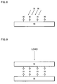
- the process of irradiating the surface of the first substrate 800a with a radical (second irradiation step) is carried out subsequently to the process of Fig. 7 .
- the step of irradiating the surface of the first substrate 800a with a nitrogen radical is carried out.
- the first irradiation step illustrated in Fig. 7 and the second irradiation step illustrated in Fig. 8 may be simultaneously carried out. Otherwise, the second irradiation step may be carried out after the first irradiation step has been completed.
- the radiation of the radical unlike the radiation of the plasma, inflicts only small damage on the surface of the substrate because it consists in radiating a particle beam which is electrically neutral and is not accelerated.
- first substrate 800a and the second substrate 800b are stacked and their surfaces are brought into mutual contact as illustrated in Fig. 9 and they are weighted as occasion demands. As a result, the first substrate 800a and the second substrate 800b can be bonded.
- the exaltation of the strength of bonding substrates in consequence of the combined use of plasma and radical is possibly related to the realization of a fine surface condition of some sort or other by the cooperation of the plasma radiation which includes accelerated particles and exerts a strong influence on the surfaces of the substrates and the radical radiation which inflicts only small damage to the surfaces of the substrates.
- the first embodiment represents the case of disposing the first substrate 800a, the first electrode 110, the second electrode 120, and the second substrate 800b sequentially in the order mentioned and simultaneously irradiating the first substrate 800a and the second substrate 800b with a plasma.
- the process illustrated in the first embodiment proves preferable from the viewpoint of realizing a highly productivity, this invention does not need to be limited to that process.
- the second embodiment represents the case of performing plasma radiation and radical radiation separately on the individual substrates.
- Like members used also in the first embodiment will be designated herein by like reference numerals. Further, since the supply of raw material gases and the process of bonding substrates in the present case are similar to those in the first embodiment, their detailed descriptions will be omitted here.
- Fig. 10 is a diagram illustrating in type section the construction of an irradiation mechanism in the substrate bonding equipment according to the present embodiment.
- Fig. 10 depicts the case of performing plasma radiation and radical radiation on the first substrate 800a, the second substrate 80bis processed similarly.
- the first substrate 800a, the first electrode 110 furnished with openings 111, and the second electrode 120 are disposed sequentially in the order mentioned as opposed to one another as illustrated in Fig. 10 .
- the second electrode is not required to be furnished with an opening.
- the control part 300 effects such a control as to ground the first electrode 110 and, at the same time, apply a high-frequency voltage to the first substrate 800a (more precisely a substrate electrode).
- a high-frequency voltage is generated in the space between the first electrode 110 and the first substrate 800a and the surface of the first substrate 800a is irradiated with this oxygen plasma.
- the control part 300 effects such a control as to ground the first electrode 110 and, at the same time, apply the high-frequency voltage to the second electrode.
- a nitrogen plasma is generated in the space between the first electrode 110 and the second electrode 120 and the first substrate 800a is irradiated with a neutral nitrogen radical which has passed the openings of the first electrode 110 in consequence of the generation of the nitrogen plasma.
- the same plasma radiation and radical radiation are carried out also on the second substrate 800b. Then, the first substrate 800a and the second substrate 800b are stacked and their surfaces are brought into mutual contact and they are bonded as weighted as occasion demands. Thus, also in the present embodiment, strong bonding of substrates can be realized.
- the first embodiment and the second embodiment represent the cases of inducing generation of oxygen plasma and nitrogen plasma by applying the high-frequency (RF) voltage during the plasma radiation and the radical radiation.
- RF high-frequency
- the method of excitation to be used for the generation of plasma does not need to be limited to the recourse to the high frequency (RF). It goes without saying that the excitation may be attained by using a varying means such as, for example, low frequency, micro-wave, helicon wave, or surface wave.
- the plasma required for the sake of the plasma radiation is generated by the application of the high-frequency (RF) voltage.
- the plasma is generated by the application of a micro-wave and, during the course of this plasma generation, the substrate is irradiated with the radical which has passed the prescribed openings.
- the supply of the raw material gases and the process for mutually stacking the substrates and weighting them for strong union are the same as those in the first embodiment. Their detailed descriptions, therefore, will be omitted here.
- Fig. 11 is a diagram illustrating in type section the construction of an irradiation mechanism in the substrate bonding apparatus of the present embodiment.
- the first substrate 800a Inside the chamber 100 shown in Fig. 11 , the first substrate 800a, the first electrode 110 which is a conductor plate furnished with a plurality of openings, and a dielectric plate 410 are disposed sequentially in the order mentioned.
- a micro-wave guide tube 420 To the dielectric plate 410, a micro-wave guide tube 420 is connected through the medium of a slot antenna part 430.
- the micro-wave guide tube 420 discharges a role of transmitting a micro-wave having a frequency of about 2.45 GHz to the dielectric plate 410 through the medium of the slot antenna part 430.
- a plasma is generated.
- the substrate bonding apparatus By the substrate bonding apparatus according to the present embodiment, the following process is carried out.
- the first electrode 110 is grounded and, at the same time, the first substrate 800a (precisely the substrate electrode) is subjected to application of the high-frequency voltage.
- the high-frequency voltage a voltage 200 V in force and 13 MHz in frequency, for example, is used.
- the first electrode 110 is grounded and, at the same time, a micro-wave is transmitted to the dielectric plate 410 by the micro-wave guide tube 420.
- a nitrogen plasma is generated in the space between the first electrode 110 and the dielectric plate 420.
- the nitrogen radical which has passed the openings of the first electrode 110 is made to irradiate the first substrate 800a.
- Fig. 11 illustrates in type section the case of effecting radical radiation.
- radiation of a nitrogen radical can be effected subsequently to the radiation of an oxygen plasma.
- the first substrate 800a and the second substrate 800b which have undergone these radiations can be mutually bonded strongly by stacking them and bringing their surfaces into close mutual contact.
- the first embodiment described above represents the case of using the first electrode 110 and the second electrode 120 thereby effecting the radiation of an oxygen plasma and the radiation of a nitrogen radical with one device.
- the present embodiment represents the case of not only radiating an oxygen plasma and radiating a nitrogen radical but also radiating such a neutral atom beam of an inert gas as an argon atom beam.
- Fig. 12 is a diagram illustrating in type section the construction of an irradiation mechanism in a substrate bonding apparatus of the present embodiment.
- the first substrate 800a, the first electrode 110, the second electrode 120 and the second substrate 800b are disposed sequentially in the order mentioned.
- the first electrode 110 and the second electrode 120 are provided respectively with a plurality of openings 111 and 121 (the first openings 111 and the second openings 121).
- the first supporting part 130 and the second supporting part 140 which are intended to support the first substrate 800a and the second substrate 800b function as a first substrate electrode and a second substrate electrode for applying voltage respectively to the first substrate 800a and the second substrate 800b. These points are similar to those involved in the first embodiment.
- the chamber 100 is provided therein with a surrounding wall member 510 and the first electrode 110 and the second electrode 120 are so disposed as to close the opposite terminals of the surrounding wall member 510.
- the surrounding wall member 510 is formed of such an electrically conductive substance as metal.
- the mutual fit between the surrounding wall member 510 and the first electrode 110 and that between the surrounding wall member 510 and the second electrode 120 are each attained through the medium of an insulating member 520. Consequently, the surrounding wall member 510, the first electrode 110, and the second electrode 120 are electrically insulated separated.
- a pair of stick inner electrodes 530 are disposed parallel as to the first electrode 110 and the second electrode 120. More specifically, the inner electrode 530 is disposed within the space which is enclosed with the first electrode 110, the second electrode 120, and the surrounding wall member 510.
- a second gas piping 540 for introducing a gas may be disposed inside the space.
- the substrate bonding apparatus 10 is furnished with the power source 210 which is intended to apply a voltage of such high frequency (RF) as, for example, about 13 MHz to each of the first substrate 800a and the second substrate 800b.
- the substrate bonding apparatus 10 is also furnished with a DC power source 550 intended to apply a direct current voltage to the pair of inner electrodes 530.
- control part 300 of the present embodiment not only controls the state of application of the voltage to the first electrode 110, the second electrode 120, the first substrate 800a, and the second substrate 800b and the state of grounding thereof but also controls the application of the voltage to the inner electrode 530 and the grounding of the surrounding wall member 510.
- control part 300 By the control which is effected by the control part 300, the state of application of the voltage to the first electrode 110, the second electrode 120, the first substrate 800a, the second substrate 800b, the inner electrode 530, and the surrounding wall member 510 and the state of grounding thereof are switched.
- this control part 300 it is made possible not only to switch the process for plasma radiation and the process for radical radiation but also to switch the process for radiation of the inert gas neutral atom beam. That is, the apparatus of the present embodiment used as a sole device suffices for realizing three kinds of radiation process, i.e. the process for plasma radiation, the process for radical radiation, and the process for neutral atom beam radiation.
- the process for neutral atom beam radiation may be carried out for the purpose of cleaning the surfaces of the substrates prior to the process for oxygen plasma radiation and the process for nitrogen radical radiation.
- the contents of the control which is effected by the control part 300 will be described below.
- the present embodiment will be described as representing the case of radiating a argon neutral atom beam.
- Fig. 13 is a diagram illustrating in type section the state which the radiation mechanism assumes when it radiates a neutral atom beam.
- the control part 300 applies a direct current voltage to the inner electrode 530 and, at the same time, effects such a control as to ground the first electrode 110, the second electrode 120, and the surrounding wall member 510.
- the direct current voltage is applied to the inner electrode 530 while the supply of argon gas through the second gas piping is in process
- the argon gas transforms to a state of plasma and generates argon ion.
- the generated argon ion by the electrical field based on the direct current voltage, is advanced to the first electrode 110 and the second electrode 120, neutralized, and made to generate an argon neutral atom beam.
- the argon neutral atom beam thus generated is passed through the openings 111 and 112 formed respectively in the first electrode 110 and the second electrode 120 andmade to irradiate the first substrate 800a and the second substrate 800b.
- the process for the plasma radiation and the process for the radical radiation are fundamentally similar to those involved in the case of the first embodiment.
- the first electrode 110, the second electrode 120, and the surrounding wall member 510 are electrically insulated, the first electrode 110 and the second electrode 120 have no possibility of being short-circuited through the medium of the surrounding wall member 510.
- the direct current voltage is applied to one pair of inner electrodes 530 and, at the same time, the first electrode 110, the second electrode 120, and the surrounding wall member 510 are grounded.
- the inner electrode 530 assumes a state of being surrounded with grounded metal members.
- the argon gas is transformed by the direct current voltage to a state of plasma and finally the argon neutral atom beam is made to irradiate the first substrate 800a and the second substrate 800b. As a result, the surfaces of the first substrate 800a and the second substrate 800b are cleaned.
- the oxygen plasma and the nitrogen radical are continuously radiated by switching the state of application of the voltage to the first electrode 110, the second electrode 120, the first substrate 800a, and the second substrate 800b and the state of grounding them. Then, finally, by stacking the first substrate 800a and the second substrate 800b and bringing their surfaces into close contact, when necessary, in a weighted state, the first substrate 800a and the second substrate 800b are bonded.
- the first electrode 110 and the second electrode 120 which are used for radiating an oxygen plasma and a nitrogen radical may be concurrently used as part of the mechanism for generating a neutral atom beam.
- the necessity for separately attaching an extra source for the generation of a neutral atombeam generation for the purpose of cleaning the first substrate 800a and the second substrate 800b ceases to exist.
- the first embodiment has represented the case of effecting radiation of a plurality of kinds of particle beam by switching the state of application of voltage to the first electrode, the second electrode, the first substrate 800a, and the second substrate 800b and the state of grounding them.
- the present embodiment is illustrated by citing the case of using a coil for the generation of inductively coupled plasma (ICP) in the place of the first electrode and the second electrode.
- ICP inductively coupled plasma
- Fig. 14 is a diagram illustrating in type section the construction of a radiation mechanism of the substrate bonding apparatus of the present embodiment.
- the first substrate 800a, a coil 610 , and the second substrate 800b are disposed sequentially in the order mentioned as opposed to one another. Since the construction of the first supporting part 130, the second supporting part 140, and the gas piping 150 is the same as that in the case of the first embodiment, it will be omitted from the following detailed description.
- the coil 610 is wound around along the parallel surfaces of the first substrate 800a and the second substrate 800b. In other words, the winding axis of the coil 610 is perpendicular to the first substrate 800a and the second substrate 800b.
- the coil 610 of this construction is what is ordinarily called a columnar coil and it is formed by winding an electric wire in several turns or so or in a still larger number.
- the coil 610 is used for the purpose of generating a high-frequency induction field.
- the coil 610 is disposed in the proximity of the intermediate point between the first substrate 800a and the second substrate 800b.
- the coil 610 is preferred to be formed in a diameter larger than the diameters of the first substrate 800a and the second substrate 800b. In other words, the coil 610 is preferred to be formed in such a diameter that the first substrate 800a and the second substrate 800b may pass through the coil 610 of an annular shape without touching the coil 610 as shown by the arrow mark in Fig. 14 .
- the substrate bonding apparatus 10 is furnished with the power source 210 for applying a high-frequency (RF) voltage of about 13 MHz to each of the first substrate 800a and the second substrate 800b and a power source 620 for applying a high-frequency voltage of about 2 MHz to the coil 610.
- Power sources capable of applying voltages of other frequencies, when necessary, may be adopted in the place of the power source 210 and the power source 620 for the coil.
- the substrate bonding apparatus 10 is furnished with the control part 300 which is intended to control the state of application of voltage to the first substrate 800a, the second substrate 800b, and the coil 610 and the state of grounding them.
- the control part 300 By the control effected by this control part 300, the state of application of voltage to the first substrate 800a and the second substrate 800b and the state of grounding them is switched. Then, by this control part 300, the process for irradiating the surfaces of the first substrate 800a and the second substrate 800b with the RF plasma and the process for irradiating the surfaces of the first substrate 800a and the second substrate 800b with the ion and/or the radical generated from the inductively coupled plasma is properly switched. Now, the contents of the control which is effected by the control part 300 will be described below.
- Fig. 15 is a diagram illustrating in type section the state which the substrate bonding apparatus 10 assumes when the radiation of the RF plasma in process.
- the control part 300 effects such a control as to apply a high-frequency voltage to the coil 610 and, at the same time, apply a voltage to the first substrate 800a and the second substrate 800b.
- the inductively coupled plasma is generated as will be specifically described herein below and, by virtue of the automatic C-bias, induced to give rise to a potential difference between the coil 610 and the first electrode 800a and between the coil 610 and the second electrode 800b.
- the RF plasma is generated each in the space between the coil 610 and the first substrate 800a and in the space between the coil 610 and the second substrate 800b.
- the RF plasma is generated in the neighborhoods of the first substrate 800a and the second substrate 800b. Then, the generated RF plasma is made to irradiate the surfaces of the first substrate 800a and the second substrate 800b.
- the oxygen plasma is generated in the space between the coil 610 and the first substrate 800a and in the space between the coil 610 and the second substrate 800b and this oxygen plasma is induced to irradiate the surfaces of the first substrate 800a and the second substrate 800b.
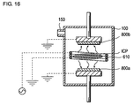
- Fig. 16 is a diagram illustrating in type section the state which the radiation mechanism assumes during the radiation of a radical and/or ion generated from an inductively coupled plasma.
- control part 300 effects such a control as to ground the first substrate 800a and the second substrate 800b and, at the same time, apply a high-frequency voltage to the coil 610.
- the application of the high-frequency voltage to the coil 610 results in generating a high-frequency induction field. Then, by the induction magnetic field which is generated by this high-frequency induction field, the electrons are accelerated and consequently enabled to generate a plasma (inductively coupled plasma) in the neighborhood of the coil 610. The ion and/or the radical or the like generated from the inductively coupled plasma are caused as by the diffusion mechanism to irradiate the surfaces of the first substrate 800a and the second substrate 800b.
- the nitrogen plasma is generated in the neighborhood of the coil 610 and the nitrogen ion and/or the nitrogen radical generated from the nitrogen plasma are induced to irradiate the surfaces of the first substrate 800a and the second substrate 800b.
- the first substrate 800a and the second substrate 800b are stacked and their surfaces which have undergone the irradiation are brought into close mutual contact to effect mutual bonding of the two substrates.
- the first substrate 800a and the second substrate 800b may be brought into mutual contact and then bonded by moving the first supporting part 130 and the second supporting part 140 in a vertical direction while keeping the first substrate 800a and the second substrate 800b held fast on the first supporting part 130 and the second supporting part 140. Since the diameter of the coil 610 is larger than the diameters of the first substrate 800a and the second substrate 800b, the first substrate 800a and the second substrate 800b can move past the inside of the coil 610. As a result, the first substrate 800a and the second substrate 800b can be bonded without suffering the first substrate 800a and the second substrate 800b to interfere with the coil 610.
- Table 1 is a diagram showing the results of a test for tensile strength performed in the present working example
- table 2 is a diagram showing the conditions for bonding substrates.
- the pressure of oxygen was set at 30 (Pa) and the pressure of nitrogen at 100 (Pa) as shown in table 2.
- the RF voltage a voltage 200 V in force and 13.4 MHz in frequency was used.
- the micro-wave power as set at 2000 W.
- the durations of the process of plasma radiation and radical radiation were each fixed at 60 seconds.
- Table 1 depicts a comparative example besides the present working example. Specifically, it shows (1) the case of sole radiation of oxygen radical, (2) the case of sole radiation of nitrogen radical, (3) the case of sole radiation of oxygen plasma, (4) the case of sole radiation of nitrogen plasma, (5) the case of sole radiation of argon ion beam, (6) the case of radiation of nitrogen plasma and subsequent radiation of oxygen radical, (7) the case of radiation of nitrogen plasma and subsequent radiation of oxygen plasma, (8) the case of radiation of oxygen radical and subsequent radiation of nitrogen radical, (9) the case of radiation of oxygen plasma and subsequent radiation of nitrogen radical (referred to as "Referential Example 1)," (10) the case of radiation of oxygen plasma and subsequent radiation of nitrogen radical (referred to as "Best Example"), (11) the case of plasma radiation of the mixture of oxygen and nitrogen (referred to as "Referential Example 2”) , and (12) the case of radical radiation of the mixture of oxygen and nitrogen.
- Table 1 shows (1) the case of sole radiation of oxygen radical, (2) the case of sole radiation of nitrogen radical, (3) the case of sole radiation of oxygen plasma,
- limit of adhesive agent refers to the case of suffering detachment of the adhesive part bonding the tensile strength tester and a substrate prior to exfoliation of the mutually bonded substrates. This detachment occurs when the substrates are in a state of being mutually bonded strongly.
- the parts which have the entry of "X" in table 1 each indicate a case of failing to bond the substrates.
- the substrates were not bonded when the oxygen plasma or the nitrogen plasma was solely radiated, when the oxygen radical or the nitrogen radical was solely radiated. They were not strongly bonded when the radiation of nitrogen plasma or nitrogen radical preceded the projection of oxygen plasma or oxygen radical.
- the substrates can be bonded comparatively strongly by subjecting them to the radiation of nitrogen radical or oxygen plasma simultaneously with or subsequently to the radiation of oxygen plasma and thereafter stacking the substrates mutually.
- the case of making the radiation "simultaneously" as mentioned herein embraces the case of mixing oxygen and nitrogen and subj ecting the produced mixture to plasma radiation (the case of Referential Example 2 mentioned above).
- the preceding description has demonstrated a novel substrate bonding technique which is expected to attain mutual bonding of substrates by performing the step for radiating nitrogen particle beam simultaneously with or subsequently to the step for radiating oxygen particle beam and thereafter stacking the substrates mutually. From a different point of view, that description may well be said to have demonstrated a novel substrate bonding technique which is expected to effect mutual bonding of the substrates by performing the radical radiation simultaneously with or subsequently to the plasma radiation and thereafter stacking the substrates mutually. Particularly, it has demonstrated an effective substrate bonding technique which consists in performing the radiation of nitrogen radical continuously after the step for radiating oxygen plasma has been completed and thereafter stacking the substrates mutually.
- the construction which is used in the first through fifth modes of embodiment with the object of irradiating substrates with plasma and radical, as novel apparatus and method for radiation by themselves, are expected to find utility not only in the field of bonding substrates but also in a wide range of fields. It enjoys prominent usefulness particularly because the radiation of plasma and the radiation of radical both can be easily and conveniently realized with one device by simply controlling the state of application of voltage to the first electrode, the second substrate, and the substrates and the state of grounding them.
- the preceding embodiment represents the case of performing the operation of bonding substrates in the air at room temperature.
- This invention does not need to limit the operation to these particular conditions.
- the operation of bonding substrates may be carried out in vacuum, for example. An experiment has shown that when silicon substrates are mutually bonded in vacuum (100°C, seven hours), they are bonded so strongly that they will not be separated from each other even by a pull with a force exceeding 27.3 MPa.
Landscapes
- Physics & Mathematics (AREA)
- Engineering & Computer Science (AREA)
- Plasma & Fusion (AREA)
- Thermal Sciences (AREA)
- Chemical & Material Sciences (AREA)
- Analytical Chemistry (AREA)
- Pressure Welding/Diffusion-Bonding (AREA)
- Plasma Technology (AREA)
- Lining Or Joining Of Plastics Or The Like (AREA)
Claims (13)
- Verfahren zum wechselseitigen Verbinden von Substraten (800), umfassend:einen ersten Bestrahlungsschritt zum Bestrahlen der Oberflächen der einzelnen Substrate (800) mit einem Sauerstoffplasma,einen zweiten Bestrahlungsschritt zum Bestrahlen der Oberflächen der Substrate (800) mit einem Stickstoffradikal gleichzeitig mit oder nach dem ersten Bestrahlungsschritt, undeinen Verbindungsschritt zum Stapeln der einzelnen Substrate (800) und zum Zusammenbringen derer Oberflächen in engen Kontakt im Anschluss an den ersten und zweiten Bestrahlungsschritt.
- Verfahren nach Anspruch 1, welches weiter einen Schritt zum Ausstrahlen eines neutralen Edelgas-Atomstrahls vor dem ersten Bestrahlungsschritt umfasst.
- Verfahren nach Anspruch 1 oder 2, wobei der erste Bestrahlungsschritt, der zweite Bestrahlungsschritt und der Verbindungsschritt im Vakuum ausgeführt werden.
- Verfahren nach einem der Ansprüche 1 bis 3, welches weiter einen Schritt zum nacheinander Anordnen eines Substrats, einer mit mindestens einer Öffnung (111) ausgestatteten ersten Elektrode (110) und einer zweiten Elektrode (120) in der genannten Reihenfolge umfasst,
wobei der erste Bestrahlungsschritt einen Schritt zum Erden der ersten Elektrode (110) enthält, während an dem Substrat eine Hochfrequenzspannung angelegt wird, damit das Erzeugen des Sauerstoffplasmas in einem Raum zwischen der ersten Elektrode (110) und dem Substrat induziert wird, und die Oberfläche des Substrats mit dem erzeugten Sauerstoffplasma bestrahlt wird, und
wobei der zweite Bestrahlungsschritt einen Schritt zum Erden der ersten Elektrode (110) enthält, während an der zweiten Elektrode (120) eine Hochfrequenzspannung angelegt wird, damit das Erzeugen des Stickstoffplasmas in einem Raum zwischen der ersten Elektrode (110) und der zweiten Elektrode (120) induziert wird, und einem Stickstoffradikal, das die mindestens eine Öffnung (111) der ersten Elektrode (110) durchlaufen hat, ermöglicht wird, in Folge der Erzeugung des Stickstoffplasmas, die Oberfläche des Substrats, zu bestrahlen. - Verfahren nach Anspruch 4, welches weiter einen Schritt zum Anlegen einer Spannung an eine innere Elektrode, die in einem Raum zwischen der ersten Elektrode (110) und der zweiten Elektrode (120) angeordnet ist, umfasst, während die erste Elektrode (110) und die zweite Elektrode (120) geerdet werden, und einem neutralen Edelgas-Atomstrahl, der die Öffnungen (111) in der ersten Elektrode (110) durchlaufen hat, ermöglicht wird, die Oberfläche des Substrats zu bestrahlen.
- Verfahren nach einem der Ansprüche 1 bis 3, welches weiter einen Schritt zum nacheinander Anordnen eines ersten Substrats (800a), einer mit einer ersten Öffnung (111) ausgestatteten ersten Elektrode (110), einer mit einer zweiten Öffnung (121) ausgestatteten zweiten Elektrode (120) und eines zweiten Substrats (800b) in der genannten Reihenfolge umfasst,
wobei der erste Bestrahlungsschritt einen Schritt zum Erden der ersten Elektrode (110) und der zweiten Elektrode (120) enthält, während an dem ersten Substrat (800a) und dem zweiten Substrat (800b) eine Hochfrequenzspannung angelegt wird, damit das Erzeugen eines Sauerstoffplasmas in einem Raum zwischen der zweiten Elektrode (120) und dem zweiten Substrat (800b) induziert und gleichzeitig die Oberflächen des ersten Substrats (800a) und des zweiten Substrats (800b) mit dem Sauerstoffplasma bestrahlt wird,
wobei der zweite Bestrahlungsschritt einen Schritt zum Erden der ersten Elektrode (110) enthält, während an der zweiten Elektrode (120) eine Hochfrequenzspannung angelegt wird, damit das Erzeugen eines Stickstoffplasmas in einem Raum zwischen der ersten Elektrode (110) und der zweiten Elektrode (120) induziert und einem Stickstoffradikal, das die erste Öffnung (111) der ersten Elektrode (110) durchlaufen hat, ermöglicht wird, in Folge der Stickstoffplasmaerzeugung, die Oberfläche des ersten Substrats (800a) zu bestrahlen, und
einem Schritt zum Erden des zweiten Substrats (800), während an der ersten Elektrode (110) eine Hochfrequenzspannung angelegt wird, damit die Erzeugung eines Stickstoffplasmas in einem Raum zwischen der ersten Elektrode (110) und der zweiten Elektrode (120) induziert wird und einem Stickstoffradikal, das die zweite Öffnung (121) der zweiten Elektrode (120) durchlaufen hat, ermöglicht wird, in Folge der Stickstoffplasmaerzeugung die Oberfläche des zweiten Substrats (800b) zu bestrahlen. - Verfahren nach einem der Ansprüche 1 bis 3, welches weiter einen Schritt zum einander entgegengesetzten Anordnen eines Substrats und einer Spule (610) umfasst,
wobei der erste Bestrahlungsschritt einen Schritt zum Anlegen einer Hochfrequenzspannung an das Substrat und an die Spule (610) enthält, damit die Erzeugung des Sauerstoffplasmas in einem Raum zwischen dem Substrat und der Spule (610) induziert und dem Sauerstoffplasma ermöglicht wird, die Oberfläche des Substrats zu bestrahlen,
wobei der zweite Bestrahlungsschritt einen Schritt zum Erden des Substrats enthält, während an der Spule (610) eine Hochfrequenzspannung angelegt wird, damit das Erzeugen eines induktiv gekoppelten Plasmas mit Stickstoff als Gaskeim in der Umgebung der Spule (610) induziert und dass einem Stickstoffion und/oder Stickstoffradikal, das in Folge des induktiv gekoppelten Plasmas erzeugt wurde, ermöglicht wird, die Oberfläche des Substrats zu bestrahlen. - Verfahren nach einem der Ansprüche 1 bis 3, welches weiter einen Schritt zum nacheinander Anordnen eines ersten Substrats (800a), einer Spule (610) und eines zweiten Substrats (800b) in der genannten Reihenfolge umfasst,
wobei der erste Schritt einen Schritt zum Anlegen einer Hochfrequenzspannung an dem ersten Substrat (800a), dem zweiten Substrat (800b) und der Spule (610) enthält, damit das Sauerstoffplasma in einem Raum zwischen dem ersten Substrat (800a) und der Spule (610) und in einem Raum zwischen dem zweiten Substrat (800b) und der Spule (610) induziert und dem Sauerstoffplasma ermöglicht wird, die Oberflächen des ersten Substrats (800a) und des zweiten Substrats (800b) zu bestrahlen, und
wobei der zweite Schritt einen Schritt zum Erden des ersten Substrats (800a) und des zweiten Substrats (800b) aufweist, während an der Spule (610) eine Hochfrequenzspannung angelegt wird, damit das Erzeugen eines induktiv gekoppelten Plasmas mit Stickstoff als Gaskeim in der Umgebung der Spule (610) induziert und einem in Folge des induktiv gekoppeltem Plasma erzeugten Stickstoffion und/oder Stickstoffradikal ermöglicht wird, die Oberflächen des ersten Substrats (800a) und des zweiten Substrats (800b) zu bestrahlen. - Substratverbindungsvorrichtung zum wechselseitigen Verbinden von Substraten (800), umfassend:eine erste Bestrahlungseinheit zum Bestrahlen der Oberflächen der einzelnen Substrate (800) mit einem Sauerstoffplasma,eine zweite Bestrahlungseinheit zum Bestrahlen der Oberflächen der einzelnen Substrate (800) mit einem Stickstoffradikal gleichzeitig mit oder nach dem Bestrahlen mit dem Sauerstoffplasma, undeine Verbindungseinheit zum Stapeln der einzelnen mit dem Sauerstoffplasma und dem Stickstoffradikal bestrahlten Substrate (800) und zum Zusammenbringen derer Oberflächen in engen Kontakt.
- Vorrichtung nach Anspruch 9, weiter umfassend:eine Kammer (100) zum Aufnehmen eines Substrats, eine mit einer Öffnung (111) ausgestattete erste Elektrode (110) und eine zweite Elektrode (120), die darin nacheinander in der genannten Reihenfolge angeordnet sind,eine Leitung zum Zuführen von Rohmaterialgasen jeweils für ein Sauerstoffplasma und Stickstoffradikal in die Kammer (100), undeine Steuereinheit (300) zum Steuern des Zustands einer elektrischen Verbindung des Substrats, der ersten Elektrode (110) und der zweiten Elektrode (120), wobei die Steuereinheit (300), bei der Einleitung einer Bestrahlung eines Sauerstoffplasmas, die erste Elektrode (110) erdet, während diese an dem Substrat eine Hochfrequenzspannung anlegt, damit diese das Erzeugen des Sauerstoffplasmas in einem Raum zwischen der ersten Elektrode (110) und dem Substrat induziert und die Oberfläche des Substrats mit dem Sauerstoffplasma bestrahlt, und diese, bei der Einleitung einer Bestrahlung eines Stickstoffradikals, die erste Elektrode (110) erdet, während sie an der zweiten Elektrode (120) eine Hochfrequenzspannung anlegt, damit sie das Erzeugen eines Stickstoffplasmas in einem Raum zwischen der ersten Elektrode (110) und der zweiten Elektrode (120) induziert und es dem in Folge der Stickstoffplasmaerzeugung durch die Öffnung (111) der ersten Elektrode durchgetretenen Stickstoffradikal ermöglicht, die Oberfläche des Substrats zu bestrahlen.
- Vorrichtung nach Anspruch 9, umfassend:eine Kammer (100) zum Aufnehmen eines ersten Substrats (800a), eine mit einer ersten Öffnung (111) ausgestattete erste Elektrode (110), eine mit einer zweiten Öffnung (121) ausgestattete zweite Elektrode (120) und ein zweites Substrat (800b), die darin nacheinander in der genannten Reihenfolge angeordnet sind,eine Leitung zum Zuführen von Rohmaterialgasen jeweils für das Sauerstoffpiasma und Stickstoffradikal in die Kammer (100), undeine Steuereinheit (300) zum Steuern des Zustands einer elektrischen Verbindung des ersten Substrats (800a), der ersten Elektrode (110), der zweiten Elektrode (120) und des zweiten Substrats (800b),wobei die Steuereinheit (300) bei der Einleitung einer Bestrahlung des Sauerstoffplasmas die erste Elektrode (110) und die zweite Elektrode (120) erdet, während diese an dem ersten Substrat (800a) und dem zweiten Substrat (800b) eine Hochfrequenzspannung anlegt, damit das Erzeugen des Sauerstoffplasmas in einem Raum zwischen der ersten Elektrode (110) und dem ersten Substrat (800a) und in einem Raum zwischen der zweiten Elektrode (120) und dem zweiten Substrat (800b) induziert und die Oberflächen des ersten Substrats (800a) und des zweiten Substrats (800b) mit dem Sauerstoffplasma bestrahlt, und diese, bei der Einleitung einer Bestrahlung der Oberfläche des ersten Substrats (800a), die erste Elektrode (110) erdet, während diese an der zweiten Elektrode (120) eine Hochfrequenzspannung anlegt, damit diese die Erzeugung der Stickstoffradikale in einem Raum zwischen der ersten Elektrode (110) und der zweiten Elektrode (120) induziert und einem durch die erste Öffnung (111) der ersten Elektrode (110) durchgetretenen Stickstoffradikal ermöglicht, die Oberfläche des ersten Substrats (800a) zu bestrahlen, und diese, bei der Einleitung einer Bestrahlung der Oberfläche des zweiten Substrats (800b) mit dem Stickstoffradikal, die zweite Elektrode (120) erdet, während diese an der ersten Elektrode (110) eine Hochfrequenzspannung anlegt, damit diese die Erzeugung des Stickstoffradikals in einem Raum zwischen der ersten Elektrode (110) und der zweiten Elektrode (120) induziert und dem die zweite Öffnung (121) der zweiten Elektrode durchlaufenen Stickstoffradikal ermöglicht, die Oberfläche des zweiten Substrats (800b) zu bestrahlen.
- Vorrichtung nach Anspruch 9, umfassend:eine Kammer (100) zum Aufnehmen eines ersten Substrats (800a), eine mit einer ersten Öffnung (111) ausgestattete erste Elektrode (110), eine mit einer zweiten Öffnung (121) ausgestatteten zweite Elektrode (120) und ein zweites Substrat (800b), die darin nacheinander in der genannten Reihenfolge angeordnet sind,eine Leitung zum Zuführen von Rohmaterialgasen jeweils für das Sauerstoffplasma und einem Stickstoffradikal in die Kammer (100), undeine Steuereinheit (300) zum Steuern des Zustands einer elektrischen Verbindung des ersten Substrats (800a), der ersten Elektrode (110), der zweiten Elektrode (120) und des zweiten Substrats (800b),wobei die Steuereinheit (300), bei der Einleitung einer Bestrahlung mit dem Sauerstoffplasma, die erste Elektrode (110) und die zweite Elektrode (120) erdet, während diese an dem ersten Substrat (800a) und dem zweiten Substrat (800b) eine Hochfrequenzspannung anlegt, damit das Erzeugen des Sauerstoffplasmas in einem Raum zwischen der ersten Elektrode (110) und dem ersten Substrat (800a) und in einem Raum zwischen der zweiten Elektrode (120) und dem zweiten Substrat (800b) induziert und diese dem Sauerstoffplasma ermöglicht, die Oberflächen des ersten Substrats (800a) und des zweiten Substrats (800b) zu bestrahlen, diese, bei der Einleitung einer Bestrahlung der Oberfläche des ersten Substrats (800a) mit dem Stickstoffradikal, die erste Elektrode (110) erdet, während diese an der zweiten Elektrode (120) eine Hochfrequenzspannung anlegt, damit diese die Erzeugung eines Stickstoffplasmas in einem Raum zwischen der ersten Elektrode (110) und der zweiten Elektrode (120) induziert und diese dem durch die erste Öffnung (111) der ersten Elektrode (110) durchlaufenen Stickstoffradikal ermöglicht, die Oberfläche des ersten Substrats (800a) zu bestrahlen, und diese, bei der Einleitung einer Bestrahlung der Oberfläche des zweiten Substrats (800b) mit dem Stickstoffradikal, die zweite Elektrode (120) erdet, während diese an die erste Elektrode (110) eine Hochfrequenzspannung anlegt, damit diese das Erzeugen des Stickstoffplasmas in einem Raum zwischen der ersten Elektrode (110) und der zweiten Elektrode (120) induziert und diese dem durch die zweite Öffnung (121) der zweiten Elektrode (120) durchlaufenen Stickstoffradikal ermöglicht, die Oberfläche des zweiten Substrats (800b) zu bestrahlen.
- Verfahren zum gegenseitigen Verbinden von Substraten (800), umfassend:einen ersten Bestrahlungsschritt zum Bestrahlen der Oberflächen der einzelnen Substrate (800) mit einem Sauerstoffplasma,einen zweiten Bestrahlungsschritt zum Bestrahlen der Oberflächen der Substrate (800) mit einem Stickstoffplasma gleichzeitig mit oder nach dem ersten Bestrahlungsschritt, undeinem Verbindungsschritt zum Stapeln der einzelnen Substrate (800) und Zusammenbringen derer Oberflächen in engen Kontakt im Anschluss an den ersten und zweiten Bestrahlungsschritt.
Applications Claiming Priority (2)
| Application Number | Priority Date | Filing Date | Title |
|---|---|---|---|
| JP2003308059A JP3980539B2 (ja) | 2003-08-29 | 2003-08-29 | 基板接合方法、照射方法、および基板接合装置 |
| JP2003308059 | 2003-08-29 |
Publications (3)
| Publication Number | Publication Date |
|---|---|
| EP1518669A2 EP1518669A2 (de) | 2005-03-30 |
| EP1518669A3 EP1518669A3 (de) | 2010-07-07 |
| EP1518669B1 true EP1518669B1 (de) | 2013-12-25 |
Family
ID=34191243
Family Applications (1)
| Application Number | Title | Priority Date | Filing Date |
|---|---|---|---|
| EP04019770.9A Expired - Lifetime EP1518669B1 (de) | 2003-08-29 | 2004-08-20 | Verfahren und Vorrichtung zum Verkleben von Substraten |
Country Status (4)
| Country | Link |
|---|---|
| US (1) | US7686912B2 (de) |
| EP (1) | EP1518669B1 (de) |
| JP (1) | JP3980539B2 (de) |
| KR (1) | KR101044391B1 (de) |
Cited By (2)
| Publication number | Priority date | Publication date | Assignee | Title |
|---|---|---|---|---|
| US12300661B2 (en) | 2020-03-31 | 2025-05-13 | Adeia Semiconductor Bonding Technologies Inc. | Reliable hybrid bonded apparatus |
| US12431460B2 (en) | 2017-04-21 | 2025-09-30 | Adeia Semiconductor Bonding Technologies Inc. | Die processing |
Families Citing this family (39)
| Publication number | Priority date | Publication date | Assignee | Title |
|---|---|---|---|---|
| WO2005055293A1 (ja) * | 2003-12-02 | 2005-06-16 | Bondtech Inc. | 接合方法及びこの方法により作成されるデバイス並びに表面活性化装置及びこの装置を備えた接合装置 |
| JP2007115825A (ja) * | 2005-10-19 | 2007-05-10 | Bondtech Inc | 表面活性化方法および表面活性化装置 |
| GB0609167D0 (en) * | 2006-05-10 | 2006-06-21 | Univ Open | Semiconductor bonding techniques |
| WO2007139994A2 (en) * | 2006-05-25 | 2007-12-06 | Objectvideo, Inc. | Intelligent video verification of point of sale (pos) transactions |
| WO2008090701A1 (ja) * | 2007-01-24 | 2008-07-31 | Konica Minolta Opto, Inc. | マイクロチップの製造方法、及びマイクロチップ基板の接合装置 |
| KR100841375B1 (ko) * | 2007-06-12 | 2008-06-26 | 삼성에스디아이 주식회사 | 접합방법 및 그를 이용한 유기전계발광표시장치의 제조방법 |
| KR100841376B1 (ko) * | 2007-06-12 | 2008-06-26 | 삼성에스디아이 주식회사 | 접합방법 및 그를 이용한 유기전계발광표시장치의 제조방법 |
| JP2009010263A (ja) * | 2007-06-29 | 2009-01-15 | Eiko Engineering Co Ltd | 基板接合装置 |
| KR100889625B1 (ko) | 2007-07-19 | 2009-03-20 | 삼성모바일디스플레이주식회사 | 접합방법 및 그를 이용한 유기전계발광표시장치의 제조방법 |
| JP5088681B2 (ja) * | 2007-10-15 | 2012-12-05 | セイコーエプソン株式会社 | 圧電振動子の製造方法 |
| FR2931585B1 (fr) * | 2008-05-26 | 2010-09-03 | Commissariat Energie Atomique | Traitement de surface par plasma d'azote dans un procede de collage direct |
| JP5985136B2 (ja) | 2009-03-19 | 2016-09-06 | ソニー株式会社 | 半導体装置とその製造方法、及び電子機器 |
| JP4659112B1 (ja) * | 2009-09-28 | 2011-03-30 | 三菱重工業株式会社 | 接合装置 |
| JP5212346B2 (ja) | 2009-12-11 | 2013-06-19 | 株式会社デンソー | プラズマ発生装置 |
| US8844793B2 (en) * | 2010-11-05 | 2014-09-30 | Raytheon Company | Reducing formation of oxide on solder |
| KR102353489B1 (ko) * | 2011-01-25 | 2022-01-19 | 에베 그룹 에. 탈너 게엠베하 | 웨이퍼들의 영구적 결합을 위한 방법 |
| DE102011013467A1 (de) * | 2011-03-09 | 2012-09-13 | Manz Ag | Vorrichtung und Verfahren zum plasmaunterstützten Behandeln zumindest zweier Substrate |
| KR101794390B1 (ko) | 2011-04-08 | 2017-12-01 | 에베 그룹 에. 탈너 게엠베하 | 웨이퍼 영구 접합 방법 |
| JP2013012564A (ja) * | 2011-06-29 | 2013-01-17 | Tokyo Electron Ltd | 表面改質装置、接合システム、表面改質方法、プログラム及びコンピュータ記憶媒体 |
| WO2014015899A1 (de) * | 2012-07-24 | 2014-01-30 | Ev Group E. Thallner Gmbh | Verfahren und vorrichtung zum permanenten bonden von wafern |
| WO2014115702A1 (ja) * | 2013-01-24 | 2014-07-31 | 株式会社日立国際電気 | 半導体装置の製造方法、基板処理装置および記録媒体 |
| CN109616408B (zh) | 2013-05-29 | 2023-07-25 | Ev 集团 E·索尔纳有限责任公司 | 用以接合衬底的装置及方法 |
| US9870922B2 (en) | 2014-04-25 | 2018-01-16 | Tadatomo Suga | Substrate bonding apparatus and substrate bonding method |
| DE102014011933A1 (de) * | 2014-08-14 | 2016-02-18 | Manz Ag | Plasmabehandlungsvorrichtung und Verfahren zur Oberflächenbehandlung von Substraten |
| JP6452199B2 (ja) * | 2015-07-16 | 2019-01-16 | 株式会社Kokusai Electric | 基板処理装置、半導体装置の製造方法およびプログラム |
| US11837444B2 (en) | 2016-11-07 | 2023-12-05 | Tadatomo Suga | Substrate joining method, substrate joining system and method for controlling hydrophilic treatment device |
| EP3367425A1 (de) * | 2017-02-28 | 2018-08-29 | IMEC vzw | Verfahren zum direkten verbinden von halbleitersubstraten |
| JP6867686B2 (ja) * | 2017-06-30 | 2021-05-12 | 株式会社 セルバック | 接合装置 |
| US10727219B2 (en) | 2018-02-15 | 2020-07-28 | Invensas Bonding Technologies, Inc. | Techniques for processing devices |
| US20210265300A1 (en) * | 2018-08-31 | 2021-08-26 | Bondtech Co., Ltd. | Bonding system and bonding method |
| KR102840203B1 (ko) | 2020-09-01 | 2025-08-01 | 삼성전자주식회사 | 기판 정렬 장치 및 이를 구비하는 기판 본딩 설비 |
| US12409644B2 (en) | 2020-09-30 | 2025-09-09 | Tadatomo Suga | Substrate bonding method and substrate bonding system |
| US12550799B2 (en) | 2021-03-31 | 2026-02-10 | Adeia Semiconductor Bonding Technologies Inc. | Direct bonding methods and structures |
| US12469683B2 (en) | 2021-09-27 | 2025-11-11 | Applied Materials Inc. | Water vapor plasma to enhance surface hydrophilicity |
| US12604771B2 (en) | 2021-10-28 | 2026-04-14 | Adeia Semiconductor Bonding Technologies Inc. | Direct bonding methods and structures |
| KR102494936B1 (ko) * | 2021-12-30 | 2023-02-06 | 세메스 주식회사 | 기판 처리 장치와 이를 포함하는 기판 접합 시스템 및 이를 이용한 기판 처리 방법 |
| KR20230105177A (ko) | 2022-01-03 | 2023-07-11 | 삼성전자주식회사 | 플라즈마 처리 장치, 이를 포함하는 기판 본딩 시스템 및 이를 이용한 기판 본딩 방법 |
| US20250096190A1 (en) * | 2023-09-20 | 2025-03-20 | Tokyo Electron Limited | Methods and devices for improving bond strength of diffusion barriers |
| JP2025144080A (ja) * | 2024-03-19 | 2025-10-02 | 株式会社Screenホールディングス | 基板接合方法および基板接合装置 |
Citations (2)
| Publication number | Priority date | Publication date | Assignee | Title |
|---|---|---|---|---|
| US6060403A (en) * | 1997-09-17 | 2000-05-09 | Kabushiki Kaisha Toshiba | Method of manufacturing semiconductor device |
| WO2003015151A1 (fr) * | 2001-08-02 | 2003-02-20 | Tokyo Electron Limited | Procede de traitement d'un materiau de base et materiau d'utlisation de dispositif electronique |
Family Cites Families (8)
| Publication number | Priority date | Publication date | Assignee | Title |
|---|---|---|---|---|
| US4598022A (en) * | 1983-11-22 | 1986-07-01 | Olin Corporation | One-step plasma treatment of copper foils to increase their laminate adhesion |
| JPH02178630A (ja) * | 1988-12-29 | 1990-07-11 | Sharp Corp | ポリイミド薄膜の製法及びその装置 |
| US5383993A (en) * | 1989-09-01 | 1995-01-24 | Nippon Soken Inc. | Method of bonding semiconductor substrates |
| JP2701709B2 (ja) * | 1993-02-16 | 1998-01-21 | 株式会社デンソー | 2つの材料の直接接合方法及び材料直接接合装置 |
| AU9296098A (en) * | 1997-08-29 | 1999-03-16 | Sharon N. Farrens | In situ plasma wafer bonding method |
| US6450116B1 (en) * | 1999-04-22 | 2002-09-17 | Applied Materials, Inc. | Apparatus for exposing a substrate to plasma radicals |
| US6902987B1 (en) * | 2000-02-16 | 2005-06-07 | Ziptronix, Inc. | Method for low temperature bonding and bonded structure |
| WO2005055293A1 (ja) * | 2003-12-02 | 2005-06-16 | Bondtech Inc. | 接合方法及びこの方法により作成されるデバイス並びに表面活性化装置及びこの装置を備えた接合装置 |
-
2003
- 2003-08-29 JP JP2003308059A patent/JP3980539B2/ja not_active Expired - Lifetime
-
2004
- 2004-08-20 EP EP04019770.9A patent/EP1518669B1/de not_active Expired - Lifetime
- 2004-08-27 US US10/928,851 patent/US7686912B2/en active Active
- 2004-08-28 KR KR1020040068233A patent/KR101044391B1/ko not_active Expired - Lifetime
Patent Citations (3)
| Publication number | Priority date | Publication date | Assignee | Title |
|---|---|---|---|---|
| US6060403A (en) * | 1997-09-17 | 2000-05-09 | Kabushiki Kaisha Toshiba | Method of manufacturing semiconductor device |
| WO2003015151A1 (fr) * | 2001-08-02 | 2003-02-20 | Tokyo Electron Limited | Procede de traitement d'un materiau de base et materiau d'utlisation de dispositif electronique |
| US20040235311A1 (en) * | 2001-08-02 | 2004-11-25 | Toshio Nakanishi | Base method treating method and electron device-use material |
Cited By (2)
| Publication number | Priority date | Publication date | Assignee | Title |
|---|---|---|---|---|
| US12431460B2 (en) | 2017-04-21 | 2025-09-30 | Adeia Semiconductor Bonding Technologies Inc. | Die processing |
| US12300661B2 (en) | 2020-03-31 | 2025-05-13 | Adeia Semiconductor Bonding Technologies Inc. | Reliable hybrid bonded apparatus |
Also Published As
| Publication number | Publication date |
|---|---|
| EP1518669A3 (de) | 2010-07-07 |
| US20050173057A1 (en) | 2005-08-11 |
| EP1518669A2 (de) | 2005-03-30 |
| KR101044391B1 (ko) | 2011-06-27 |
| US7686912B2 (en) | 2010-03-30 |
| JP3980539B2 (ja) | 2007-09-26 |
| KR20050022953A (ko) | 2005-03-09 |
| JP2005079353A (ja) | 2005-03-24 |
Similar Documents
| Publication | Publication Date | Title |
|---|---|---|
| US7686912B2 (en) | Method for bonding substrates and method for irradiating particle beam to be utilized therefor | |
| US5571366A (en) | Plasma processing apparatus | |
| US8662010B2 (en) | Plasma processing apparatus, plasma processing method, plasma film deposition apparatus, and plasma film deposition method | |
| US20010022293A1 (en) | Plasma processing equipment and plasma processing method using the same | |
| EP1323180A2 (de) | System, vorrichtung und verfahren zur waferbehandlung unter verwendung von monofrequenz-rf-leistung in einer plasma-bhandlungskammer | |
| JP3561080B2 (ja) | プラズマ処理装置及びプラズマ処理方法 | |
| KR101883247B1 (ko) | 플라스마 처리 장치 및 플라스마 처리 방법 | |
| TW200913019A (en) | Plasma doping apparatus and plasma doping method | |
| US20150194290A1 (en) | Plasma processing apparatus | |
| JP2928577B2 (ja) | プラズマ処理方法およびその装置 | |
| JPH08115901A (ja) | プラズマ処理方法およびプラズマ処理装置 | |
| JP3881307B2 (ja) | プラズマ処理装置 | |
| JP3276023B2 (ja) | プラズマ処理装置の制御方法 | |
| EP3748668B1 (de) | Reaktive ionenätzvorrichtung | |
| US20050258148A1 (en) | Plasma system with isolated radio-frequency powered electrodes | |
| JP2002531914A (ja) | プラズマ浸漬イオン注入用増強プラズマモード、方法およびシステム | |
| JP2002110649A (ja) | プラズマ処理装置 | |
| JPH07122398A (ja) | プラズマ処理装置 | |
| JP3082659B2 (ja) | プラズマ処理装置 | |
| JP3662211B2 (ja) | プラズマ処理装置 | |
| JP3687474B2 (ja) | プラズマ処理装置 | |
| JP4527833B2 (ja) | プラズマ処理装置および方法 | |
| JPH1167493A (ja) | プラズマ処理装置及びプラズマ処理方法 | |
| JPH05125547A (ja) | プラズマ処理装置 | |
| JP2002305184A (ja) | 半導体製造装置 |
Legal Events
| Date | Code | Title | Description |
|---|---|---|---|
| PUAI | Public reference made under article 153(3) epc to a published international application that has entered the european phase |
Free format text: ORIGINAL CODE: 0009012 |
|
| AK | Designated contracting states |
Kind code of ref document: A2 Designated state(s): AT BE BG CH CY CZ DE DK EE ES FI FR GB GR HU IE IT LI LU MC NL PL PT RO SE SI SK TR |
|
| AX | Request for extension of the european patent |
Extension state: AL HR LT LV MK |
|
| PUAL | Search report despatched |
Free format text: ORIGINAL CODE: 0009013 |
|
| AK | Designated contracting states |
Kind code of ref document: A3 Designated state(s): AT BE BG CH CY CZ DE DK EE ES FI FR GB GR HU IE IT LI LU MC NL PL PT RO SE SI SK TR |
|
| AX | Request for extension of the european patent |
Extension state: AL HR LT LV MK |
|
| RIC1 | Information provided on ipc code assigned before grant |
Ipc: B32B 38/00 20060101ALI20100531BHEP Ipc: H05H 1/24 20060101ALI20100531BHEP Ipc: H01J 37/32 20060101ALI20100531BHEP Ipc: H01L 21/18 20060101ALI20100531BHEP Ipc: B32B 37/18 20060101AFI20100531BHEP |
|
| 17P | Request for examination filed |
Effective date: 20101025 |
|
| AKX | Designation fees paid |
Designated state(s): AT BE BG CH CY CZ DE DK EE ES FI FR GB GR HU IE IT LI LU MC NL PL PT RO SE SI SK TR |
|
| 17Q | First examination report despatched |
Effective date: 20110324 |
|
| RAP1 | Party data changed (applicant data changed or rights of an application transferred) |
Owner name: BONDTECH CO., LTD. Owner name: SUGA, TADATOMO Owner name: AYUMI INDUSTRY CO., LTD. |
|
| GRAP | Despatch of communication of intention to grant a patent |
Free format text: ORIGINAL CODE: EPIDOSNIGR1 |
|
| INTG | Intention to grant announced |
Effective date: 20130719 |
|
| GRAS | Grant fee paid |
Free format text: ORIGINAL CODE: EPIDOSNIGR3 |
|
| GRAA | (expected) grant |
Free format text: ORIGINAL CODE: 0009210 |
|
| AK | Designated contracting states |
Kind code of ref document: B1 Designated state(s): AT BE BG CH CY CZ DE DK EE ES FI FR GB GR HU IE IT LI LU MC NL PL PT RO SE SI SK TR |
|
| REG | Reference to a national code |
Ref country code: GB Ref legal event code: FG4D |
|
| REG | Reference to a national code |
Ref country code: CH Ref legal event code: EP |
|
| REG | Reference to a national code |
Ref country code: DE Ref legal event code: R081 Ref document number: 602004044056 Country of ref document: DE Owner name: BONDTECH CO., LTD, KYOTO-SHI, JP Free format text: FORMER OWNERS: SUGA, TADATOMO, TOKIO/TOKYO, JP; AYUMI INDUSTRY CO., LTD., HIMEJI, HYOGO, JP Ref country code: DE Ref legal event code: R081 Ref document number: 602004044056 Country of ref document: DE Owner name: AYUMI INDUSTRY CO., LTD., HIMEJI, JP Free format text: FORMER OWNERS: SUGA, TADATOMO, TOKIO/TOKYO, JP; AYUMI INDUSTRY CO., LTD., HIMEJI, HYOGO, JP Ref country code: DE Ref legal event code: R081 Ref document number: 602004044056 Country of ref document: DE Owner name: SUGA, TADATOMO, JP Free format text: FORMER OWNERS: SUGA, TADATOMO, TOKIO/TOKYO, JP; AYUMI INDUSTRY CO., LTD., HIMEJI, HYOGO, JP |
|
| REG | Reference to a national code |
Ref country code: AT Ref legal event code: REF Ref document number: 646385 Country of ref document: AT Kind code of ref document: T Effective date: 20140115 |
|
| REG | Reference to a national code |
Ref country code: IE Ref legal event code: FG4D |
|
| REG | Reference to a national code |
Ref country code: DE Ref legal event code: R096 Ref document number: 602004044056 Country of ref document: DE Effective date: 20140213 |
|
| PG25 | Lapsed in a contracting state [announced via postgrant information from national office to epo] |
Ref country code: FI Free format text: LAPSE BECAUSE OF FAILURE TO SUBMIT A TRANSLATION OF THE DESCRIPTION OR TO PAY THE FEE WITHIN THE PRESCRIBED TIME-LIMIT Effective date: 20131225 Ref country code: SE Free format text: LAPSE BECAUSE OF FAILURE TO SUBMIT A TRANSLATION OF THE DESCRIPTION OR TO PAY THE FEE WITHIN THE PRESCRIBED TIME-LIMIT Effective date: 20131225 |
|
| REG | Reference to a national code |
Ref country code: NL Ref legal event code: VDEP Effective date: 20131225 |
|
| REG | Reference to a national code |
Ref country code: AT Ref legal event code: MK05 Ref document number: 646385 Country of ref document: AT Kind code of ref document: T Effective date: 20131225 |
|
| PG25 | Lapsed in a contracting state [announced via postgrant information from national office to epo] |
Ref country code: BE Free format text: LAPSE BECAUSE OF FAILURE TO SUBMIT A TRANSLATION OF THE DESCRIPTION OR TO PAY THE FEE WITHIN THE PRESCRIBED TIME-LIMIT Effective date: 20131225 Ref country code: EE Free format text: LAPSE BECAUSE OF FAILURE TO SUBMIT A TRANSLATION OF THE DESCRIPTION OR TO PAY THE FEE WITHIN THE PRESCRIBED TIME-LIMIT Effective date: 20131225 |
|
| PG25 | Lapsed in a contracting state [announced via postgrant information from national office to epo] |
Ref country code: CY Free format text: LAPSE BECAUSE OF FAILURE TO SUBMIT A TRANSLATION OF THE DESCRIPTION OR TO PAY THE FEE WITHIN THE PRESCRIBED TIME-LIMIT Effective date: 20131225 Ref country code: NL Free format text: LAPSE BECAUSE OF FAILURE TO SUBMIT A TRANSLATION OF THE DESCRIPTION OR TO PAY THE FEE WITHIN THE PRESCRIBED TIME-LIMIT Effective date: 20131225 Ref country code: PL Free format text: LAPSE BECAUSE OF FAILURE TO SUBMIT A TRANSLATION OF THE DESCRIPTION OR TO PAY THE FEE WITHIN THE PRESCRIBED TIME-LIMIT Effective date: 20131225 Ref country code: RO Free format text: LAPSE BECAUSE OF FAILURE TO SUBMIT A TRANSLATION OF THE DESCRIPTION OR TO PAY THE FEE WITHIN THE PRESCRIBED TIME-LIMIT Effective date: 20131225 Ref country code: AT Free format text: LAPSE BECAUSE OF FAILURE TO SUBMIT A TRANSLATION OF THE DESCRIPTION OR TO PAY THE FEE WITHIN THE PRESCRIBED TIME-LIMIT Effective date: 20131225 Ref country code: CZ Free format text: LAPSE BECAUSE OF FAILURE TO SUBMIT A TRANSLATION OF THE DESCRIPTION OR TO PAY THE FEE WITHIN THE PRESCRIBED TIME-LIMIT Effective date: 20131225 Ref country code: ES Free format text: LAPSE BECAUSE OF FAILURE TO SUBMIT A TRANSLATION OF THE DESCRIPTION OR TO PAY THE FEE WITHIN THE PRESCRIBED TIME-LIMIT Effective date: 20131225 Ref country code: SK Free format text: LAPSE BECAUSE OF FAILURE TO SUBMIT A TRANSLATION OF THE DESCRIPTION OR TO PAY THE FEE WITHIN THE PRESCRIBED TIME-LIMIT Effective date: 20131225 Ref country code: PT Free format text: LAPSE BECAUSE OF FAILURE TO SUBMIT A TRANSLATION OF THE DESCRIPTION OR TO PAY THE FEE WITHIN THE PRESCRIBED TIME-LIMIT Effective date: 20140428 |
|
| REG | Reference to a national code |
Ref country code: DE Ref legal event code: R097 Ref document number: 602004044056 Country of ref document: DE |
|
| PG25 | Lapsed in a contracting state [announced via postgrant information from national office to epo] |
Ref country code: DK Free format text: LAPSE BECAUSE OF FAILURE TO SUBMIT A TRANSLATION OF THE DESCRIPTION OR TO PAY THE FEE WITHIN THE PRESCRIBED TIME-LIMIT Effective date: 20131225 |
|
| PLBE | No opposition filed within time limit |
Free format text: ORIGINAL CODE: 0009261 |
|
| STAA | Information on the status of an ep patent application or granted ep patent |
Free format text: STATUS: NO OPPOSITION FILED WITHIN TIME LIMIT |
|
| 26N | No opposition filed |
Effective date: 20140926 |
|
| REG | Reference to a national code |
Ref country code: DE Ref legal event code: R097 Ref document number: 602004044056 Country of ref document: DE Effective date: 20140926 |
|
| PG25 | Lapsed in a contracting state [announced via postgrant information from national office to epo] |
Ref country code: LU Free format text: LAPSE BECAUSE OF FAILURE TO SUBMIT A TRANSLATION OF THE DESCRIPTION OR TO PAY THE FEE WITHIN THE PRESCRIBED TIME-LIMIT Effective date: 20140820 Ref country code: MC Free format text: LAPSE BECAUSE OF FAILURE TO SUBMIT A TRANSLATION OF THE DESCRIPTION OR TO PAY THE FEE WITHIN THE PRESCRIBED TIME-LIMIT Effective date: 20131225 |
|
| REG | Reference to a national code |
Ref country code: CH Ref legal event code: PL |
|
| GBPC | Gb: european patent ceased through non-payment of renewal fee |
Effective date: 20140820 |
|
| PG25 | Lapsed in a contracting state [announced via postgrant information from national office to epo] |
Ref country code: CH Free format text: LAPSE BECAUSE OF NON-PAYMENT OF DUE FEES Effective date: 20140831 Ref country code: LI Free format text: LAPSE BECAUSE OF NON-PAYMENT OF DUE FEES Effective date: 20140831 |
|
| REG | Reference to a national code |
Ref country code: IE Ref legal event code: MM4A |
|
| PG25 | Lapsed in a contracting state [announced via postgrant information from national office to epo] |
Ref country code: SI Free format text: LAPSE BECAUSE OF FAILURE TO SUBMIT A TRANSLATION OF THE DESCRIPTION OR TO PAY THE FEE WITHIN THE PRESCRIBED TIME-LIMIT Effective date: 20131225 |
|
| PG25 | Lapsed in a contracting state [announced via postgrant information from national office to epo] |
Ref country code: GB Free format text: LAPSE BECAUSE OF NON-PAYMENT OF DUE FEES Effective date: 20140820 |
|
| REG | Reference to a national code |
Ref country code: FR Ref legal event code: PLFP Year of fee payment: 12 |
|
| PG25 | Lapsed in a contracting state [announced via postgrant information from national office to epo] |
Ref country code: IE Free format text: LAPSE BECAUSE OF NON-PAYMENT OF DUE FEES Effective date: 20140820 |
|
| REG | Reference to a national code |
Ref country code: DE Ref legal event code: R082 Ref document number: 602004044056 Country of ref document: DE Representative=s name: MEHLER ACHLER PATENTANWAELTE, DE Ref country code: DE Ref legal event code: R082 Ref document number: 602004044056 Country of ref document: DE Representative=s name: MEHLER ACHLER PATENTANWAELTE PARTNERSCHAFT MBB, DE Ref country code: DE Ref legal event code: R081 Ref document number: 602004044056 Country of ref document: DE Owner name: BONDTECH CO., LTD, KYOTO-SHI, JP Free format text: FORMER OWNERS: AYUMI INDUSTRY CO., LTD., HIMEJI, HYOGO, JP; BONDTECH CO., LTD, UJI-CITY, KYOTO, JP; SUGA, TADATOMO, TOKYO, JP Ref country code: DE Ref legal event code: R081 Ref document number: 602004044056 Country of ref document: DE Owner name: AYUMI INDUSTRY CO., LTD., HIMEJI, JP Free format text: FORMER OWNERS: AYUMI INDUSTRY CO., LTD., HIMEJI, HYOGO, JP; BONDTECH CO., LTD, UJI-CITY, KYOTO, JP; SUGA, TADATOMO, TOKYO, JP Ref country code: DE Ref legal event code: R081 Ref document number: 602004044056 Country of ref document: DE Owner name: SUGA, TADATOMO, JP Free format text: FORMER OWNERS: AYUMI INDUSTRY CO., LTD., HIMEJI, HYOGO, JP; BONDTECH CO., LTD, UJI-CITY, KYOTO, JP; SUGA, TADATOMO, TOKYO, JP |
|
| REG | Reference to a national code |
Ref country code: FR Ref legal event code: CA Effective date: 20160222 |
|
| PG25 | Lapsed in a contracting state [announced via postgrant information from national office to epo] |
Ref country code: BG Free format text: LAPSE BECAUSE OF FAILURE TO SUBMIT A TRANSLATION OF THE DESCRIPTION OR TO PAY THE FEE WITHIN THE PRESCRIBED TIME-LIMIT Effective date: 20131225 |
|
| PG25 | Lapsed in a contracting state [announced via postgrant information from national office to epo] |
Ref country code: GR Free format text: LAPSE BECAUSE OF FAILURE TO SUBMIT A TRANSLATION OF THE DESCRIPTION OR TO PAY THE FEE WITHIN THE PRESCRIBED TIME-LIMIT Effective date: 20140326 Ref country code: IT Free format text: LAPSE BECAUSE OF FAILURE TO SUBMIT A TRANSLATION OF THE DESCRIPTION OR TO PAY THE FEE WITHIN THE PRESCRIBED TIME-LIMIT Effective date: 20131225 |
|
| PG25 | Lapsed in a contracting state [announced via postgrant information from national office to epo] |
Ref country code: HU Free format text: LAPSE BECAUSE OF FAILURE TO SUBMIT A TRANSLATION OF THE DESCRIPTION OR TO PAY THE FEE WITHIN THE PRESCRIBED TIME-LIMIT; INVALID AB INITIO Effective date: 20040820 Ref country code: TR Free format text: LAPSE BECAUSE OF FAILURE TO SUBMIT A TRANSLATION OF THE DESCRIPTION OR TO PAY THE FEE WITHIN THE PRESCRIBED TIME-LIMIT Effective date: 20131225 |
|
| REG | Reference to a national code |
Ref country code: FR Ref legal event code: PLFP Year of fee payment: 13 |
|
| REG | Reference to a national code |
Ref country code: FR Ref legal event code: PLFP Year of fee payment: 14 |
|
| REG | Reference to a national code |
Ref country code: FR Ref legal event code: PLFP Year of fee payment: 15 |
|
| REG | Reference to a national code |
Ref country code: DE Ref legal event code: R082 Ref document number: 602004044056 Country of ref document: DE Representative=s name: WSL PATENTANWAELTE PARTNERSCHAFT MBB, DE |
|
| PGFP | Annual fee paid to national office [announced via postgrant information from national office to epo] |
Ref country code: FR Payment date: 20230822 Year of fee payment: 20 Ref country code: DE Payment date: 20230822 Year of fee payment: 20 |
|
| REG | Reference to a national code |
Ref country code: DE Ref legal event code: R071 Ref document number: 602004044056 Country of ref document: DE |