EP1517339A2 - Systéme optique d'éclairage et appareil d'exposition - Google Patents
Systéme optique d'éclairage et appareil d'exposition Download PDFInfo
- Publication number
- EP1517339A2 EP1517339A2 EP04001822A EP04001822A EP1517339A2 EP 1517339 A2 EP1517339 A2 EP 1517339A2 EP 04001822 A EP04001822 A EP 04001822A EP 04001822 A EP04001822 A EP 04001822A EP 1517339 A2 EP1517339 A2 EP 1517339A2
- Authority
- EP
- European Patent Office
- Prior art keywords
- light
- exposure apparatus
- optical system
- arc
- reflection mask
- Prior art date
- Legal status (The legal status is an assumption and is not a legal conclusion. Google has not performed a legal analysis and makes no representation as to the accuracy of the status listed.)
- Withdrawn
Links
- 230000003287 optical effect Effects 0.000 title claims abstract description 82
- 238000005286 illumination Methods 0.000 title claims abstract description 40
- 238000003384 imaging method Methods 0.000 claims abstract description 43
- 230000000873 masking effect Effects 0.000 claims description 28
- 238000000034 method Methods 0.000 claims description 16
- 210000001747 pupil Anatomy 0.000 claims description 10
- 239000000758 substrate Substances 0.000 claims description 3
- 230000007246 mechanism Effects 0.000 claims description 2
- 239000004065 semiconductor Substances 0.000 description 9
- 238000004519 manufacturing process Methods 0.000 description 7
- 239000000463 material Substances 0.000 description 7
- 238000009826 distribution Methods 0.000 description 6
- 230000005284 excitation Effects 0.000 description 6
- 239000007788 liquid Substances 0.000 description 6
- 239000002184 metal Substances 0.000 description 4
- 230000008569 process Effects 0.000 description 4
- 238000001816 cooling Methods 0.000 description 3
- 230000009467 reduction Effects 0.000 description 3
- 238000012360 testing method Methods 0.000 description 3
- 238000012546 transfer Methods 0.000 description 3
- 238000001444 catalytic combustion detection Methods 0.000 description 2
- 238000013461 design Methods 0.000 description 2
- 238000005530 etching Methods 0.000 description 2
- 239000011521 glass Substances 0.000 description 2
- 239000002245 particle Substances 0.000 description 2
- 238000000926 separation method Methods 0.000 description 2
- 241000276498 Pollachius virens Species 0.000 description 1
- 239000006096 absorbing agent Substances 0.000 description 1
- 238000009825 accumulation Methods 0.000 description 1
- 230000005540 biological transmission Effects 0.000 description 1
- 230000015572 biosynthetic process Effects 0.000 description 1
- 230000008859 change Effects 0.000 description 1
- 238000006243 chemical reaction Methods 0.000 description 1
- 230000001427 coherent effect Effects 0.000 description 1
- 239000013078 crystal Substances 0.000 description 1
- 238000011161 development Methods 0.000 description 1
- 238000010586 diagram Methods 0.000 description 1
- 230000000694 effects Effects 0.000 description 1
- 239000007943 implant Substances 0.000 description 1
- 238000007689 inspection Methods 0.000 description 1
- 238000005468 ion implantation Methods 0.000 description 1
- 239000004973 liquid crystal related substance Substances 0.000 description 1
- 238000010297 mechanical methods and process Methods 0.000 description 1
- 230000003647 oxidation Effects 0.000 description 1
- 238000007254 oxidation reaction Methods 0.000 description 1
- 238000004806 packaging method and process Methods 0.000 description 1
- 238000000206 photolithography Methods 0.000 description 1
- 229920002120 photoresistant polymer Polymers 0.000 description 1
- 230000005855 radiation Effects 0.000 description 1
- 238000011084 recovery Methods 0.000 description 1
- 238000004064 recycling Methods 0.000 description 1
- 238000007789 sealing Methods 0.000 description 1
- 229910052710 silicon Inorganic materials 0.000 description 1
- 239000010703 silicon Substances 0.000 description 1
- 230000001960 triggered effect Effects 0.000 description 1
- XLYOFNOQVPJJNP-UHFFFAOYSA-N water Substances O XLYOFNOQVPJJNP-UHFFFAOYSA-N 0.000 description 1
Images


Classifications
-
- G—PHYSICS
- G03—PHOTOGRAPHY; CINEMATOGRAPHY; ANALOGOUS TECHNIQUES USING WAVES OTHER THAN OPTICAL WAVES; ELECTROGRAPHY; HOLOGRAPHY
- G03F—PHOTOMECHANICAL PRODUCTION OF TEXTURED OR PATTERNED SURFACES, e.g. FOR PRINTING, FOR PROCESSING OF SEMICONDUCTOR DEVICES; MATERIALS THEREFOR; ORIGINALS THEREFOR; APPARATUS SPECIALLY ADAPTED THEREFOR
- G03F7/00—Photomechanical, e.g. photolithographic, production of textured or patterned surfaces, e.g. printing surfaces; Materials therefor, e.g. comprising photoresists; Apparatus specially adapted therefor
- G03F7/20—Exposure; Apparatus therefor
-
- G—PHYSICS
- G03—PHOTOGRAPHY; CINEMATOGRAPHY; ANALOGOUS TECHNIQUES USING WAVES OTHER THAN OPTICAL WAVES; ELECTROGRAPHY; HOLOGRAPHY
- G03F—PHOTOMECHANICAL PRODUCTION OF TEXTURED OR PATTERNED SURFACES, e.g. FOR PRINTING, FOR PROCESSING OF SEMICONDUCTOR DEVICES; MATERIALS THEREFOR; ORIGINALS THEREFOR; APPARATUS SPECIALLY ADAPTED THEREFOR
- G03F7/00—Photomechanical, e.g. photolithographic, production of textured or patterned surfaces, e.g. printing surfaces; Materials therefor, e.g. comprising photoresists; Apparatus specially adapted therefor
- G03F7/70—Microphotolithographic exposure; Apparatus therefor
- G03F7/70058—Mask illumination systems
- G03F7/702—Reflective illumination, i.e. reflective optical elements other than folding mirrors, e.g. extreme ultraviolet [EUV] illumination systems
-
- G—PHYSICS
- G21—NUCLEAR PHYSICS; NUCLEAR ENGINEERING
- G21K—TECHNIQUES FOR HANDLING PARTICLES OR IONISING RADIATION NOT OTHERWISE PROVIDED FOR; IRRADIATION DEVICES; GAMMA RAY OR X-RAY MICROSCOPES
- G21K2201/00—Arrangements for handling radiation or particles
- G21K2201/06—Arrangements for handling radiation or particles using diffractive, refractive or reflecting elements
Definitions
- the present invention relates generally to an exposure apparatus, and more particularly to an exposure apparatus that uses a light source in an extreme ultraviolet (“EUV”) or X-ray region with a wavelength between 10 nm and 200 nm to expose an object, such as a single crystal substrate for a semiconductor wafer, and a glass plate for a liquid crystal display (“LCD").
- EUV extreme ultraviolet
- LCD liquid crystal display
- a reduction projection exposure method that uses, for example, EUV light or X-ray have been proposed as one of methods for manufacturing semiconductor circuit devices having a fine pattern (see, for example, Japanese Patent Application Publication No. 10-70058 (or its U.S. counterpart, U.S. Patent No. 6, 504, 896B1), Japanese Patent Application Publication No. 2003-045774 (or its U.S. counterpart, U.S. Patent Application Publication No. 2003031017A1), and Japanese Patent Application Publication No. 2003-045784 (or its U.S. counterpart, U.S. Patent Application Publication No. 2003031017A1).
- This method uses the EUV light to illuminate a mask (or a reticle) that forms a circuit pattern, and projects a reduced size of the pattern on the mask, onto a wafer surface, and to expose photoresist on the wafer surface for pattern transfer.
- FIG. 12 schematically shows principal part of a conventional EUV reduction projection exposure apparatus 1000.
- 1001 denotes an EUV light emission point
- 1002 denotes EUV light
- 1003 denotes a filter
- 1004 denotes a first rotational paraboloid mirror
- 1005 denotes a reflection-type or reflection integrator
- 1006 denotes a second rotational paraboloid mirror
- 1007 denotes a reflection mask
- 1008 denotes plural mirrors that constitute a projection optical system
- 1009 denotes a wafer
- 1010 denotes a mask stage
- 1011 denotes a wafer stage
- 1012 denotes an arc aperture
- 1013 denotes a laser light source
- 1014 denotes a laser condensing optical system
- 1017 denotes a vacuum container.
- FIG. 14 is a plane view showing a relationship between an illuminated area 1015 on the mask 1007 and an arc area 1016 to be exposed.
- the exposure apparatus 1000 thus includes a light source section 1013, 1014 that generates the EUV light, an illumination optical system (i.e., the first rotational paraboloid mirror 1004, the reflection integrator 1005 and the second rotational paraboloid mirror 1006), the reflection mask 1007, the projection optical system 1008, the wafer 1009, the mask mounted stage 1010, the wafer mounted stage 1011, an alignment mechanism (not shown) for precise alignment between mask and wafer positions, the vacuum container 1017 that maintains vacuum of the entire optical system vacuum for reduced attenuations of the EUV light, and an exhaust apparatus (not shown).
- an illumination optical system i.e., the first rotational paraboloid mirror 1004, the reflection integrator 1005 and the second rotational paraboloid mirror 1006
- the reflection mask 1007 i.e., the first rotational paraboloid mirror 1004, the reflection integrator 1005 and the second rotational paraboloid mirror 1006
- the reflection mask 1007 i.e., the first rotational paraboloid mirror 1004, the reflection integrator 100
- the illumination optical system uses the first rotational paraboloid mirror 1004 to condense the EUV light 1002 from the emission point 1001 into the reflection integrator 1005 so as to form secondary light sources, and uses the second rotational paraboloid mirror 1006 to superimpose and condense the EUV light from these secondary light sources so as to uniformly illuminate the mask 1007.
- the reflection mask 1007 forms a pattern to be transferred, using a non-reflected part made of an EUV absorber on a multilayer mirror.
- the projection optical system 1008 images, on the wafer 1009, the EUV light that has information of a circuit pattern reflected by the reflection mask 1007.
- the projection optical system 1008 is configured to have excellent imaging performance in an off-axis, thin arc area (i.e. , apart from an optical-axis center).
- the aperture 1012 with the arc opening just prior to the wafer 1009 enables exposure to use only this thin arc area.
- the exposure scans the reflection mask 1007 and the wafer 1009 simultaneously and transfers a rectangular shot on the entire surface of the mask.
- the projection optical system 1008 is comprised of plural multilayer mirrors, and configured to project a reduced size of pattern on the mask 1007 onto the wafer 1009 surface.
- the projection optical system 1008 typically forms an image-side telecentric system, and usually provides an object side (or the reflection mask side) with a non-telecentric structure so as to avoid physical interference with the illumination light incident upon the reflection mask 1007.
- the laser condensing optical system 1014 condenses a laser beam from the laser light source 1013 onto a target (not shown) at the emission point 1001, generating a high-temperature plasma light source 1001.
- the EUV light 1002 thermally radiated from this plasma light source is reflected on the first rotational paraboloid mirror 1004 and turns into parallel EUV light. This light is reflected on the reflection integrator 1005 and forms a multiplicity of secondary light sources.
- the EUV light from these secondary light sources is reflected on the second rotational paraboloid mirror 1006 and illuminates the reflection mask 1007.
- Distances from the secondary light sources to the second rotational paraboloid mirror 1006 and from the secondary rotational paraboloid mirror 1006 to the reflection mask 1007 are set to be equal to a focal distance of the second rotational paraboloid mirror 1006.
- the projection optical system 1008 is configured to project an image of the secondary light sources onto an entrance pupil surface, and thereby meets the Kohler's illumination conditions.
- the EUV light that illuminates one point on the reflection mask 1007 is superimposed EUV beams emitted from all the secondary light sources.
- the illuminated area 1015 on the mask surface is similar, as shown in FIG. 13, to a plane shape of a concave or convex mirror as an element in the reflection integrator 1005, and it is an approximately rectangular shape that includes the arc shape 1016 to be actually exposed.
- the projection optical system 1008 is configured to project an image of the secondary light sources onto its pupil surface.
- the conventional EUV reduction projection exposure apparatus has been disadvantageous, because the aperture 1012 that defines an illuminated area is provided near the wafer 1009 and should be somewhat apart from the driving wafer during exposure. This separation defocuses the exposure area.
- an exemplary object of the present invention to provide an exposure apparatus, which clarifies an imaging system between an reticle and an aperture for defining an illuminated area, and includes an illumination optical system that has the imaging system.
- an exposure apparatus of one aspect according to the present invention includes an illumination optical system for illuminating a pattern of a reflection mask, by using light from a light source, wherein the illumination optical system includes a field stop that defines an illuminated area on the reflection mask, and has an opening, and an imaging system for directing the light from the opening in the field stop into the reflection mask, the imaging system being a coaxial optical system, and a projection optical system for projecting the pattern on the reflection mask onto a substrate, wherein a principal ray of the imaging system at a side of the reflection mask forming an inclination angle to a common axis of the coaxial optical system, the inclination angle being approximately equal to an angle between a principal ray of the projection optical system at the side of the reflection mask and a normal to a surface of the reflection mask.
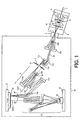
- FIG. 1 is a schematic view of an embodiment according to the present invention.
- FIG. 2 is a view of an integrator that receives parallel light.
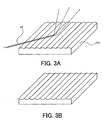
- FIG. 3A is a schematic view of a reflection integrator having plural convex cylindrical surfaces
- FIG. 3B is a schematic view of a reflection integrator having plural concave cylindrical surfaces.
- FIG. 4 is a view of a sectional shape of the integrator.
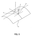
- FIG. 5 is a view for explaining an angular distribution of light reflected on a cylindrical surface.
- FIG. 6 is a view showing an arc area formed by the light reflected on the cylindrical surface.
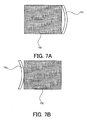
- FIG. 7A is a view in a scan exposure start state
- FIG. 7B is a view in a scan exposure end state.
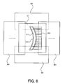
- FIG. 8 is a schematic view of a variable arc slit and a masking blade.
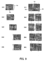
- FIG. 9 is a view showing actions of the masking blade during scan exposure.
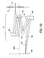
- FIG. 10 is a schematic view of a masking imaging system.
- FIG. 11A is a view showing an aperture stop corresponding to a large ⁇ mode in a normal illumination
- FIG. 11B is a view showing an aperture stop corresponding to a small ⁇ mode in a normal illumination
- FIG. 11C is a view showing an aperture stop corresponding to an annular illumination mode
- FIG. 11D is a view showing an aperture stop corresponding to a quadrupole illumination mode.
- FIG. 12 is a schematic view of a prior art illustration.
- FIG. 13 is a schematic perspective view of a conventional reflection integrator.
- FIG. 14 is a view of a conventional illuminated area and an arc area to be exposed.
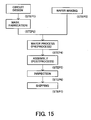
- FIG. 15 is a flowchart for explaining a method for fabricating devices (semiconductor chips such as ICs, LSIs, and the like, LCDs, CCDs, etc.).
- FIG. 16 is a detailed flowchart for Step 4 of wafer process shown in FIG. 15.
- FIG. 1 is a schematic view of an embodiment according to the present invention.
- 1 denotes an excitation laser beam.
- 2 denotes a plasma emission point.
- 3a denotes a nozzle that injects a liquid drop as a target for plasma generations, and 3b denotes a liquid-drop recovery part for recovering and recycling liquid drops that have not received excitation laser beam.
- 4 denotes a condenser mirror that receives light emitted from the plasma emission point.
- 6a denotes a filter that removes flying particles (or debris) from the plasma
- 6b denotes a wavelength filter that removes light other than the EUV light.
- 7 denotes a pinhole aperture arranged at or near the condensed point of the condenser mirror 4.
- 8 denotes a vacuum container that accommodates the plasma light source. These elements constitute a light source section.
- 5 denotes the EUV light condensed by the mirror 4.
- 9 denotes a connector that connects an exposure apparatus body to a plasma light source section in a vacuum state.
- 10a and 10b are part of a parallelizing optical system that receives the EUV light through the aperture 7, converts it into parallel light, and includes a concave mirror and a convex mirror.
- 11a is an integrator having plural cylindrical mirrors
- 11b and 11c are part of an optical system that includes a rotational paraboloid mirror for condensing the light from the integrator 11a into an arc shape.
- 12, 13 constitute a slit system (or a field stop) wherein 12 denotes a slit that has an arc opening and a partially variable width.
- 13 denotes a masking blade for restricting the illumination light to a desired exposed area, located on a surface conjugate to the reflection mask 16.
- 14 denotes a masking imaging system that images at a desired magnification with respect to the masking blade 13 as the object side and the reflection mask 16 as the image side, and forms an arc illuminated area on the reflection mask.
- 14a, 14b, 14c and 14d, respectively, denote a curved mirror in the masking imaging system 14, and 14e is a plane mirror that reflects light from the imaging system 14 to 14d to reflect the image-side light 14' of the masking imaging system 14 for entry into the reflection mask 16 at a predetermined angle.
- 15 denotes an aperture stop located at a pupil surface in the masking imaging system 14a to 14d.
- 17 denotes a mask stage that holds the reflection mask 16.
- 18 denotes a projection optical system that includes plural mirrors, forms a coaxial optical system, and provides an object side with non-telecentricity and an image side with telecentricity.
- 19 denotes a wafer that applies a photosensitive material.
- 20 denotes a wafer stage that holds the wafer 19
- 21 denotes a vacuum container that maintains the entire optical system in the vacuum atmosphere for reduced attenuation of the EUV light.
- the excitation pulse laser beam 1 irradiates liquid drops to generate the high-temperature plasma from the emission point 2, and the thermal radiation from this plasma generates the EUV light.
- the target may use Xe liquid drops as a target
- the target may use Xe gas injected into a vacuum, a cluster generated from an adiabatic expansion, solidified Xe gas that has been cooled on the metal surface, and a metal tape, such as Cu.
- the EUV light source can use an undulator, or a so-called discharge method, such as Z pinch method, a plasma focus, a capillary discharge, and hollow cathode triggered Z pinch.
- the EUV light irradiated from the plasma emission point 2 is condensed by the condenser mirror 4, such as a rotational spheroid mirror, and taken out as a EUV beam.
- the filter 6a removes flying particles (or debris) that fly ahead directly from the plasma and its vicinity, and the filter 6b removes an unnecessary wavelength component for the EUV exposure, as required.
- the light is condensed into the pinhole aperture 7 provided on a boundary surface between the vacuum container 8 that accommodates the plasma light source, and the vacuum container 21 that accommodates the exposure apparatus body.
- the connector 9 connects the vacuum container 8 that accommodates the light source to the vacuum container 21 that accommodates the exposure apparatus body.
- the EUV light 5 that has passed through the aperture 7 is converted into approximately parallel light 10' by the parallelizing optical system that includes a concave mirror 10a that has an opening at its center, and a convex mirror 10b that has a smaller diameter than the concave mirror 10a.
- the concave mirror 10a has an opening for light reflected by the convex mirror 10b, and its opening is located on the optical axis of the EUV light from the light source.
- These mirrors 10a and 10b have a reflective surface of approximately rotational symmetry with respect to the optical axis of the EUV light from the light source.
- the center axis approximately accords with the optical axis of the EUV light.
- the above condenser mirror 4, and the mirrors 10a and 10b form a reflective multilayer for effectively reflect the EUV light, and become at high temperature during exposure since they absorb the radiant energy from the high-temperature plasma 2. Therefore, they are made of a material with high thermal conductivity, such as metal, and have cooling means (not shown), such as water cooling, for continuous cooling during exposure.
- a reflective surface of each mirror in the optical system forms a reflective multilayer to effectively reflect the EUV light
- the mirror can be made of a material with high thermal conductivity, such as metal, as required.
- the EUV light 10' that has been converted into approximately parallel light enters the integrator 11a that has plural reflective cylindrical mirrors, and the plane mirror 11b and the rotational paraboloid mirror 11c condense, into an arc shape, divergent beams divided by each cylindrical surface, thereby forming an arc illuminated area that has uniform light intensity distribution on the opening in the arc slit 12.
- FIG. 3A is a typical perspective view of the reflection convex cylindrical integrator 11a having plural convex cylindrical surfaces which receives parallel light, and the approximately parallel EUV light 10' enters in the illustrated direction.
- FIG. 3B is a typical perspective view of a reflection concave cylindrical integrator having plural concave cylindrical surfaces that exhibit similar effects to FIG. 3A.
- the integrator 11a in FIG. 1 is a reflection convex cylindrical integrator, as shown in FIG. 3A, but it may be a reflection concave cylindrical integrator shown in FIG. 3B or a combination thereof.
- FIG. 4 is a typical sectional view of the reflection convex cylindrical integrator
- FIG. 5 is a view for explaining reflections of the EUV light on the cylindrical surface of the reflection convex cylindrical integrator
- FIG. 6 is an angular distribution diagram of the EUV light reflected the reflection convex cylindrical integrator.
- reference numeral 11a denotes the reflection convex cylindrical integrator.
- the secondary light source is formed near the integrator surface and the EUV light radiated from this secondary light source has a cone angular distribution. Then the arc illumination is available by reflecting the EUV light on the mirror that has a focal point at a position of this secondary light source, and illuminating the reflection mask or a surface conjugate with the reflection mask.
- this secondary light source exists as a real image outside the reflective surface, whereas when the integrator has a convex cylindrical surface, this secondary light source exits as a virtual image inside the reflective surface.
- the ray vector P2 exists as an arc 601 having a center angle of 4 ⁇ on the xy plane as shown in FIG. 6.
- the secondary light source emits the cone divergent light, which is then reflected on the mirror having the focal distance f and then converted into parallel light.
- the reflected light is a sheet beam having an arc section with a radius f x cos ⁇ and a center angle of 2 ⁇ . Therefore, as shown in FIG. 6, only the arc area 601 is illuminated with a radius of f x cos ⁇ and a center angle of 2 ⁇ on the illuminated surface.
- FIG. 2 a description will be given of the integrator 11a that arranges a multiplicity of cylindrical surfaces in parallel on a large area, and receives the parallel light 10' with a certain beam diameter in a direction shown in FIG. 1.
- 11a is the above integrator
- 11b is a plane mirror
- 11c is a rotational paraboloid mirror
- 12 is a slit having an arc opening.
- the rotational paraboloid mirror 11c is a mirror that is centrically symmetrical around a shaft 201AX, and has a reflective surface that is part of a surface formed by rotating a paraboloid having a focal point 202 around an axis 201AX.
- a distance between the focal point 202 and the mirror effective part's center point 204 is the focal distance f.
- a distance between the point 204 and the arc slit 12 is set to be approximately equal to the focal distance f.
- the rotational paraboloid mirror 11c is arranged so that its rotational axis 201AX is arranged parallel to the reflective surface on or near the reflective surface of the integrator 11a, and aligned with the cylindrical surfaces.
- the plane mirror 11b is located between the effective part's center point 204 and the focal point 202 on the rotational paraboloid mirror 11c, the point 202' that is symmetrical to the focal point 202 with respect to the reflective surface of the mirror 11b can be located approximately at a center position of the reflective surface's effective part on the integrator 11a.
- an optical path length from the position 204 to the position 202' is equal to the focal distance f.
- This arrangement provides the position 202' and the arc slit 12 with a separation by the focal distance f from the rotational paraboloid mirror 11b or a relationship of the Fourier conversion surface. Therefore, the approximately parallel EUV light 10' incident upon the integrator 11a as illustrated is condensed at or near the opening of the arc slit 12.
- the EUV light to the rotational paraboloid mirror 11c has a low incident angle ⁇ of the primary ray between 0° and 45°, more specifically, 20°.
- the arc illuminated area maintains uniform light intensity since the multiple cylindrical surfaces on the integrator 11a superimpose the light. In other words, this can achieve effective and uniform arc illumination.
- the masking blade 13 partially restricts the arc illuminated area formed near the opening in the arc slit 12, and the masking imaging system 14 enlarges or reduces the arc illuminated area at a desired magnification.
- the reflection mask 16 is illuminated with an arc shape by introducing the arc illuminated area at a desired incident angle into the reflection mask 16 held by the mask stage 17.
- the center of curvature of the arc illuminated area accords with the optical axis 18AX of the projection optical system 18.
- the circuit pattern is exposed when the projection optical system 18 projects, onto the wafer 19 that applies a photosensitive material, at a magnification suitable for exposure, the reflected EUV light having circuit pattern information from the reflection mask 16 that has been illuminated in an arc shape.
- the above wafer is fixed on the wafer stage 20, which serves to provide back and forth and up and down parallel movements on the paper surface under control of distance measuring equipment, such as a laser interferometer (not shown).
- the scan exposure over the entire surface requires, for example, the reflection mask 16 to be scanned at a speed v in a direction parallel to the paper surface and the wafer 19 to be simultaneously synchronously scanned at a speed v / M in the direction parallel to the paper, where M is a magnification of the projection optical system 18.
- the projection optical system 18 is comprised of plural multilayer reflective mirrors, and provided with excellent imaging performance in an off-axis, thin arc area.
- the projection optical system 18 is configured to project a reduced size of the pattern on the mask 16 onto the wafer 19 surface, and form an image-side (or wafer-side) telecentric system.
- the projection optical system 1008 provides an object side (or the reflection mask side) with a non-telecentric structure so as to avoid physical interference with the illumination light incident upon the reflection mask 16, and the instant embodiment inclines the image-side principal ray, for example, by about 6° relative to the normal direction of the mask 16.
- FIGS. 7A and 7B show scan exposure start and end states on the wafer surface, respectively.
- 701 denotes an arc illuminated area on the wafer surface.
- 702 denotes an exposed area as an object to be exposed.
- the exposure area 702 moves from left to right on the paper when the wafer stage is driven.
- the arc illuminated area 701 is configured to relatively scan the exposed area 702.
- the masking blade works so that the arc illuminated area 701 is prevented from illuminating part except for the exposure area 702 at the exposure start and exposure end. This will be described in the operation of the masking blade.
- the above is applicable to scan exposure in a relatively reverse direction to the scanned direction in this embodiment.
- 810 denotes a multiple movable edges for partially changing a slit width 811 in the arc slit 12.
- 811 denotes a slit opening for forming the arc illuminated area.
- 812 denotes an arc illuminated area formed by the above integrator 11a and mirror system 11b and 11c, and this illuminated area defines light that passes through the slit opening 811.
- the uneven exposure occurs if there is uneven light intensity in the arc slit when the scan exposure transfers a reduced size of the circuit pattern in the reflection mask 16 onto the wafer 19.
- One solution for this problem uses a drive system (not shown) to move the movable edges 810 to narrow only the slit width that provides relatively strong light intensity in the arc slit, and to reduce the light amount for the scan exposure by a desired amount. As a result, exposure with uniform intensity is available on the entire exposed surface as a result of accumulation.
- the masking blade 13 includes four light-shielding plates 801, 802, 803 and 804, the upper and lower light-shielding plates 803 and 804 shield light at both ends of the arc illuminated area 812 in the arc slit opening 812, and define a longitudinal width (or a scan width) of the exposed area 702 shown in FIG. 7A.
- the light-shielding plates 801 and 802 define a lateral width (or a scan length) in the exposed area 702 by moving in a lateral direction and opening and closing an aperture from the exposure start to the exposure end for one shot in the scan exposure, as described in detail below, with reference to FIG. 9.
- (A1) to (A5) time-sequentially represent scan exposure from a start to an end, while (B1) to (B5) show actions of light-shielding plates 801 and 802 in the masking blade 13 at states (A1) to (A5).
- the exposure is about to start at the state (A1), and the light-shielding plate 802 starts to move to the right at the state (B1) to open the aperture.
- the arc illuminated area 701 is light-shielded in this state, and not actually illuminated although illustrated.
- the scan exposure starts as shown in (A2)
- the light-shielding plate 802 moves as shown in the state (B2) so as to light-shield a projection the arc illuminated area 701 from the exposure area 702.
- the arc illuminated area 701 moves within the exposed area 702 for scan exposure
- the light-shielding plate 802 moves to the right as shown in (B3) to completely open the slit opening 811.
- the light-shielding plate 801 moves to the right so as to light-shield a projection of the arc illuminated area 701 from the exposed area 702.
- the light-shielding plate 801 moves and completely shields the slit opening 811. The above series of actions provides the scan exposure for a desired exposed area.
- the masking imaging system 14 is an imaging optical system that uses the above masking blade 13 as an image surface, and the reflection mask 16 (at a position 102 in the figure) as an image surface, and includes reflective multilayer mirrors.
- This imaging system is a coaxial optical system that serves to image and form an arc illuminated area suitable for the projection optical system 18 by applying a desired magnification to the object-side arc area that arranges the common axis (or optical axis) 10A nearly at a center.
- 14a, 14b, 14c and 14d are concave or convex spherical or aspheric mirrors that use the center axis 10AX for rotational symmetry, and are concave, concave, convex and concave from 14a in the instant embodiment.
- the pupil surface in the masking imaging system 14 is located on or near the reflective surface of the mirror 14b, at which the aperture stop 15 is located.
- the aperture stop 15 changes its opening pattern to change a convergent angle (or a so-called coherence factor ⁇ ) of the illumination light at the reflection mask side, or to provide modified illumination, as described in detail below:
- the incident light condenses into the image surface 102 through the above four mirrors and aperture stop 15.
- the image side has a non-telecentric structure, and an incident angle 101 upon the image surface 102 of the principal ray 103 (or an angle between the principal ray 103 and the rotationally symmetrical axis 10AX) is set to be approximately equal to the inclination angle of the object-side principal ray of the projection optical system 18 to the mask-surface normal.
- an angle between the mask-side principal ray of the imaging system 14a to 14d and the rotationally symmetrical axis 10AX, corresponding to each position on the reflection mask's illuminated area is set to be approximately equal to an angle between the mask-side principal ray of the projection optical system and the normal to the mask surface.
- the instant embodiment sets the incident angle 101 to be about 6°, equal to the angle between the mask-side principal ray of the projection optical system 18 and the normal to the mask surface. Since the optical axis 18X of the projection optical system is parallel to the normal to the mask surface, an angle between the optical axis 18X of the projection optical system and the mask-side principal ray of the projection optical system 18.
- the angle between the mask-side principal ray of the imaging system and the optical axis of the imaging system is approximately equal to the angle between the angle between the mask-side principal ray of the projection optical system and the normal to the mask surface.
- the imaging surface properly corrects defocus at the image side, and the spot diameter on the image surface is designed to be 5 mm or smaller, preferably 1 mm or smaller.
- the plane mirror 14e reflects the image-side light 14' of the masking imaging system 14 shown in FIG. 1 and angles it toward the reflection mask 16, an orientation of an arc illuminated area formed by the light 14' is reversed and the arc's center accords with an intersection between the center axis 18AX of the projection system 18 and the reflection mask.
- the above incident angle 101 enables the principal ray of the light 14' to approximately accord with the principal ray of the object-side light 18' of the projection optical system 18 with respect to a reflective surface on the reflection mask.
- FIGS. 11A to 11D are views of exemplary opening shapes of the aperture stop 15.
- a stop in FIG. 11A has a circular opening and corresponds to a large ⁇ mode in a normal illumination.
- a stop in FIG. 11B has a circular opening smaller than the stop in FIG. 11A and corresponds to a small ⁇ mode in a normal illumination.
- a stop in FIG. 11C has an annular opening and corresponds to the annular illumination mode.
- a stop in FIG. 11D has four openings and corresponds to the quadrupole illumination mode.
- FIG. 15 is a manufacture flow for explaining a fabrication of devices (i.e. , semiconductor chips such as IC and LSI, LCDs, CCDs, etc.).
- a fabrication of a semiconductor chip As an example.
- Step 1 circuit design
- Step 2 mask fabrication
- Step 3 wafer making
- Step 4 wafer process
- a pretreatment forms actual circuitry on the wafer through photolithography using the mask and wafer.
- Step 5 (assembly), which is also referred to as a posttreatment, forms into a semiconductor chip the wafer formed in Step 4 and includes an assembly step ( e.g., dicing, bonding), a packaging step (chip sealing), and the like.
- Step 6 (inspection) performs various tests for the semiconductor device made in Step 5, such as a validity test and a durability test. Through these steps, a semiconductor device is finished and shipped (Step 7).
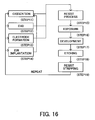
- FIG. 16 is a detailed flow of the above wafer process.
- Step 11 oxidation
- Step 12 CVD
- Step 13 electrode formation
- Step 14 ion implantation
- Step 15 resist process
- Step 16 exposure
- Step 17 development
- Step 18 etching
- Step 19 resist stripping
- the present invention is applicable to another illumination optical system that uses different light, for example, light in an EUV or E-ray region with a wavelength between 10 nm and 200 nm.
- No glass material is applicable as a lens for light with a wavelength between 20 and 50 nm, and the optical system should include mirrors only. Therefore, the present invention is effectively applicable to the illumination optical system that uses this region.
- An exposure apparatus includes an illumination optical system for illuminating a reflection mask that forms a pattern, by using light from a light source, wherein the illumination optical system includes a field stop that defines an illuminated area on the reflection mask, and has an opening, and an imaging system for introducing the light from the opening in the field stop into the reflection mask, the imaging system being a coaxial optical system, wherein a principal ray of the imaging system at a side of the reflection mask forming an inclination angle to a common axis of the coaxial optical system, the inclination angle being approximately equal to an angle between a principal ray of the projection optical system at the side of the reflection mask and a normal to a surface of the reflection mask.
Landscapes
- Physics & Mathematics (AREA)
- General Physics & Mathematics (AREA)
- Exposure And Positioning Against Photoresist Photosensitive Materials (AREA)
- Exposure Of Semiconductors, Excluding Electron Or Ion Beam Exposure (AREA)
Applications Claiming Priority (2)
| Application Number | Priority Date | Filing Date | Title |
|---|---|---|---|
| JP2003324639 | 2003-09-17 | ||
| JP2003324639A JP4241281B2 (ja) | 2003-09-17 | 2003-09-17 | 露光装置 |
Publications (2)
| Publication Number | Publication Date |
|---|---|
| EP1517339A2 true EP1517339A2 (fr) | 2005-03-23 |
| EP1517339A3 EP1517339A3 (fr) | 2009-06-10 |
Family
ID=34191311
Family Applications (1)
| Application Number | Title | Priority Date | Filing Date |
|---|---|---|---|
| EP04001822A Withdrawn EP1517339A3 (fr) | 2003-09-17 | 2004-01-28 | Systéme optique d'éclairage et appareil d'exposition |
Country Status (5)
| Country | Link |
|---|---|
| US (2) | US7110084B2 (fr) |
| EP (1) | EP1517339A3 (fr) |
| JP (1) | JP4241281B2 (fr) |
| KR (1) | KR100687655B1 (fr) |
| TW (1) | TWI267127B (fr) |
Families Citing this family (13)
| Publication number | Priority date | Publication date | Assignee | Title |
|---|---|---|---|---|
| JP4241295B2 (ja) * | 2003-09-26 | 2009-03-18 | キヤノン株式会社 | ステージ装置 |
| JP4458330B2 (ja) * | 2003-12-26 | 2010-04-28 | キヤノン株式会社 | 光源ユニットの多層膜ミラーを交換する方法 |
| JP2005317611A (ja) * | 2004-04-27 | 2005-11-10 | Canon Inc | 露光方法及び装置 |
| EP1875292A2 (fr) * | 2005-04-26 | 2008-01-09 | Carl Zeiss SMT AG | Systeme d'eclairage pour appareil d'exposition microlithographique |
| US8873021B2 (en) * | 2005-06-14 | 2014-10-28 | Koninklijke Philips N.V. | Debris mitigation system with improved gas distribution |
| US20070016163A1 (en) * | 2005-06-28 | 2007-01-18 | Microchips, Inc. | Medical and dental implant devices for controlled drug delivery |
| KR100729263B1 (ko) * | 2005-07-14 | 2007-06-15 | 삼성전자주식회사 | 기판 노광 장치 |
| JP4986754B2 (ja) * | 2007-07-27 | 2012-07-25 | キヤノン株式会社 | 照明光学系及びそれを有する露光装置 |
| JP2009176838A (ja) * | 2008-01-22 | 2009-08-06 | Canon Inc | 液浸露光装置及びデバイス製造方法 |
| DE102008001553B4 (de) * | 2008-05-05 | 2015-04-30 | Carl Zeiss Smt Gmbh | Komponente zur Einstellung einer scanintegrierten Beleuchtungsenergie in einer Objektebene einer Mikrolithographie-Projektionsbelichtungsanlage |
| US8227778B2 (en) * | 2008-05-20 | 2012-07-24 | Komatsu Ltd. | Semiconductor exposure device using extreme ultra violet radiation |
| JP5534910B2 (ja) * | 2009-04-23 | 2014-07-02 | ギガフォトン株式会社 | 極端紫外光源装置 |
| US12401779B1 (en) * | 2024-04-09 | 2025-08-26 | DISTANCE TECHNOLOGIES Oy | Calibrating optical combiner using structured light |
Family Cites Families (27)
| Publication number | Priority date | Publication date | Assignee | Title |
|---|---|---|---|---|
| DE3787035T2 (de) * | 1986-03-12 | 1994-03-10 | Matsushita Electric Ind Co Ltd | Optisches Projektionssystem für Präzisionskopien. |
| JPS6329930A (ja) | 1986-07-23 | 1988-02-08 | Nec Corp | 縮小投影露光装置 |
| JP3111476B2 (ja) * | 1991-01-08 | 2000-11-20 | 日本電気株式会社 | 照明光学装置 |
| US5581605A (en) * | 1993-02-10 | 1996-12-03 | Nikon Corporation | Optical element, production method of optical element, optical system, and optical apparatus |
| JP3371512B2 (ja) | 1994-02-23 | 2003-01-27 | 株式会社ニコン | 照明装置及び露光装置 |
| US5677939A (en) * | 1994-02-23 | 1997-10-14 | Nikon Corporation | Illuminating apparatus |
| KR0135834B1 (ko) * | 1994-10-28 | 1998-04-24 | 김광호 | 램프의 그림자를 없애기 위한 이중 반사경을 구비한 광원 장치 |
| US5737137A (en) * | 1996-04-01 | 1998-04-07 | The Regents Of The University Of California | Critical illumination condenser for x-ray lithography |
| JP3862347B2 (ja) * | 1996-04-11 | 2006-12-27 | キヤノン株式会社 | X線縮小露光装置およびこれを利用したデバイス製造方法 |
| JP3706691B2 (ja) * | 1996-08-26 | 2005-10-12 | キヤノン株式会社 | X線縮小投影露光装置及びこれを用いた半導体デバイス製造方法 |
| AU1053199A (en) * | 1997-11-14 | 1999-06-07 | Nikon Corporation | Exposure apparatus and method of manufacturing the same, and exposure method |
| JP4238390B2 (ja) * | 1998-02-27 | 2009-03-18 | 株式会社ニコン | 照明装置、該照明装置を備えた露光装置および該露光装置を用いて半導体デバイスを製造する方法 |
| JPH11345761A (ja) * | 1998-05-29 | 1999-12-14 | Nikon Corp | 走査型露光装置 |
| JP2000091220A (ja) * | 1998-09-08 | 2000-03-31 | Nikon Corp | 投影露光装置及び投影露光方法 |
| JP2000089000A (ja) | 1998-09-14 | 2000-03-31 | Nikon Corp | X線発生装置 |
| JP2000100685A (ja) | 1998-09-17 | 2000-04-07 | Nikon Corp | 露光装置及び該装置を用いた露光方法 |
| JP2003506881A (ja) | 1999-07-30 | 2003-02-18 | カール ツァイス シュティフトゥング トレイディング アズ カール ツァイス | Euv照明光学系の射出瞳における照明分布の制御 |
| JP2002023055A (ja) * | 2000-07-10 | 2002-01-23 | Nikon Corp | 結像光学系および該結像光学系を備えた露光装置 |
| JP2003015040A (ja) * | 2001-07-04 | 2003-01-15 | Nikon Corp | 投影光学系および該投影光学系を備えた露光装置 |
| TW594847B (en) * | 2001-07-27 | 2004-06-21 | Canon Kk | Illumination system, projection exposure apparatus and method for manufacturing a device provided with a pattern to be exposed |
| JP3605053B2 (ja) | 2001-07-27 | 2004-12-22 | キヤノン株式会社 | 照明光学系、露光装置及びデバイス製造方法 |
| JP3605055B2 (ja) * | 2001-07-31 | 2004-12-22 | キヤノン株式会社 | 照明光学系、露光装置及びデバイス製造方法 |
| JP2003227914A (ja) * | 2002-01-31 | 2003-08-15 | Canon Inc | Euv光用の波面分割素子及びそれを有する位相測定装置 |
| JP2003233005A (ja) * | 2002-02-07 | 2003-08-22 | Canon Inc | 反射型投影光学系、露光装置及びデバイス製造方法 |
| JP3720788B2 (ja) * | 2002-04-15 | 2005-11-30 | キヤノン株式会社 | 投影露光装置及びデバイス製造方法 |
| US20040080815A1 (en) * | 2002-07-12 | 2004-04-29 | Peter Muys | Lens with optimized heat transfer properties |
| JP2004138926A (ja) * | 2002-10-21 | 2004-05-13 | Nikon Corp | 投影光学系および該投影光学系を備えた露光装置 |
-
2003
- 2003-09-17 JP JP2003324639A patent/JP4241281B2/ja not_active Expired - Fee Related
-
2004
- 2004-01-28 EP EP04001822A patent/EP1517339A3/fr not_active Withdrawn
- 2004-01-29 TW TW093102016A patent/TWI267127B/zh not_active IP Right Cessation
- 2004-01-30 US US10/769,373 patent/US7110084B2/en not_active Expired - Fee Related
- 2004-01-30 US US10/768,896 patent/US7064806B2/en not_active Expired - Fee Related
- 2004-09-17 KR KR1020040074612A patent/KR100687655B1/ko not_active Expired - Fee Related
Non-Patent Citations (1)
| Title |
|---|
| None |
Also Published As
| Publication number | Publication date |
|---|---|
| KR100687655B1 (ko) | 2007-02-28 |
| US20050057738A1 (en) | 2005-03-17 |
| EP1517339A3 (fr) | 2009-06-10 |
| KR20050028848A (ko) | 2005-03-23 |
| US7064806B2 (en) | 2006-06-20 |
| US20050057737A1 (en) | 2005-03-17 |
| TWI267127B (en) | 2006-11-21 |
| TW200512805A (en) | 2005-04-01 |
| JP4241281B2 (ja) | 2009-03-18 |
| JP2005093693A (ja) | 2005-04-07 |
| US7110084B2 (en) | 2006-09-19 |
Similar Documents
| Publication | Publication Date | Title |
|---|---|---|
| US6919951B2 (en) | Illumination system, projection exposure apparatus and device manufacturing method | |
| US7126757B2 (en) | Illumination apparatus, exposure apparatus using the same, and device fabricating method | |
| US20060175556A1 (en) | Illumination optical system, exposure apparatus, and device manufacturing method | |
| JP3057998B2 (ja) | 照明装置及びそれを用いた投影露光装置 | |
| US20080143987A1 (en) | Exposure apparatus and device fabrication method | |
| JP3605055B2 (ja) | 照明光学系、露光装置及びデバイス製造方法 | |
| US7064806B2 (en) | Illumination optical system and exposure apparatus | |
| EP1591833A2 (fr) | Méthode d'exposition et appareil | |
| JP3605053B2 (ja) | 照明光学系、露光装置及びデバイス製造方法 | |
| US8149386B2 (en) | Illumination optical system, exposure apparatus using the same and device manufacturing method | |
| JP2005109304A (ja) | 照明光学系及び露光装置 | |
| US20050105290A1 (en) | Illumination optical system and exposure apparatus | |
| US7292316B2 (en) | Illumination optical system and exposure apparatus having the same | |
| EP1517338A2 (fr) | Système optique d'éclairage et appareil d'exposition | |
| JP2004140390A (ja) | 照明光学系、露光装置及びデバイス製造方法 | |
| JP2004170869A (ja) | 結像光学系、露光装置および露光方法 | |
| TWI245324B (en) | Projection optical system | |
| JP2005072513A (ja) | 露光装置および露光方法 |
Legal Events
| Date | Code | Title | Description |
|---|---|---|---|
| PUAI | Public reference made under article 153(3) epc to a published international application that has entered the european phase |
Free format text: ORIGINAL CODE: 0009012 |
|
| AK | Designated contracting states |
Kind code of ref document: A2 Designated state(s): AT BE BG CH CY CZ DE DK EE ES FI FR GB GR HU IE IT LI LU MC NL PT RO SE SI SK TR |
|
| AX | Request for extension of the european patent |
Extension state: AL LT LV MK |
|
| PUAL | Search report despatched |
Free format text: ORIGINAL CODE: 0009013 |
|
| AK | Designated contracting states |
Kind code of ref document: A3 Designated state(s): AT BE BG CH CY CZ DE DK EE ES FI FR GB GR HU IE IT LI LU MC NL PT RO SE SI SK TR |
|
| AX | Request for extension of the european patent |
Extension state: AL LT LV MK |
|
| 17P | Request for examination filed |
Effective date: 20091210 |
|
| AKX | Designation fees paid |
Designated state(s): DE IT NL |
|
| 17Q | First examination report despatched |
Effective date: 20100209 |
|
| STAA | Information on the status of an ep patent application or granted ep patent |
Free format text: STATUS: THE APPLICATION HAS BEEN WITHDRAWN |
|
| 18W | Application withdrawn |
Effective date: 20150327 |