EP1517339A2 - Illumination optical system and exposure apparatus - Google Patents
Illumination optical system and exposure apparatus Download PDFInfo
- Publication number
- EP1517339A2 EP1517339A2 EP04001822A EP04001822A EP1517339A2 EP 1517339 A2 EP1517339 A2 EP 1517339A2 EP 04001822 A EP04001822 A EP 04001822A EP 04001822 A EP04001822 A EP 04001822A EP 1517339 A2 EP1517339 A2 EP 1517339A2
- Authority
- EP
- European Patent Office
- Prior art keywords
- light
- exposure apparatus
- optical system
- arc
- reflection mask
- Prior art date
- Legal status (The legal status is an assumption and is not a legal conclusion. Google has not performed a legal analysis and makes no representation as to the accuracy of the status listed.)
- Withdrawn
Links
Images


Classifications
-
- G—PHYSICS
- G03—PHOTOGRAPHY; CINEMATOGRAPHY; ANALOGOUS TECHNIQUES USING WAVES OTHER THAN OPTICAL WAVES; ELECTROGRAPHY; HOLOGRAPHY
- G03F—PHOTOMECHANICAL PRODUCTION OF TEXTURED OR PATTERNED SURFACES, e.g. FOR PRINTING, FOR PROCESSING OF SEMICONDUCTOR DEVICES; MATERIALS THEREFOR; ORIGINALS THEREFOR; APPARATUS SPECIALLY ADAPTED THEREFOR
- G03F7/00—Photomechanical, e.g. photolithographic, production of textured or patterned surfaces, e.g. printing surfaces; Materials therefor, e.g. comprising photoresists; Apparatus specially adapted therefor
- G03F7/20—Exposure; Apparatus therefor
-
- G—PHYSICS
- G03—PHOTOGRAPHY; CINEMATOGRAPHY; ANALOGOUS TECHNIQUES USING WAVES OTHER THAN OPTICAL WAVES; ELECTROGRAPHY; HOLOGRAPHY
- G03F—PHOTOMECHANICAL PRODUCTION OF TEXTURED OR PATTERNED SURFACES, e.g. FOR PRINTING, FOR PROCESSING OF SEMICONDUCTOR DEVICES; MATERIALS THEREFOR; ORIGINALS THEREFOR; APPARATUS SPECIALLY ADAPTED THEREFOR
- G03F7/00—Photomechanical, e.g. photolithographic, production of textured or patterned surfaces, e.g. printing surfaces; Materials therefor, e.g. comprising photoresists; Apparatus specially adapted therefor
- G03F7/70—Microphotolithographic exposure; Apparatus therefor
- G03F7/70058—Mask illumination systems
- G03F7/702—Reflective illumination, i.e. reflective optical elements other than folding mirrors, e.g. extreme ultraviolet [EUV] illumination systems
-
- G—PHYSICS
- G21—NUCLEAR PHYSICS; NUCLEAR ENGINEERING
- G21K—HANDLING OF PARTICLES OR IONISING RADIATION NOT OTHERWISE PROVIDED FOR; IRRADIATION DEVICES; GAMMA RAY OR X-RAY MICROSCOPES
- G21K2201/00—Arrangements for handling radiation or particles
- G21K2201/06—Arrangements for handling radiation or particles using diffractive, refractive or reflecting elements
Definitions
- the present invention relates generally to an exposure apparatus, and more particularly to an exposure apparatus that uses a light source in an extreme ultraviolet (“EUV”) or X-ray region with a wavelength between 10 nm and 200 nm to expose an object, such as a single crystal substrate for a semiconductor wafer, and a glass plate for a liquid crystal display (“LCD").
- EUV extreme ultraviolet
- LCD liquid crystal display
- a reduction projection exposure method that uses, for example, EUV light or X-ray have been proposed as one of methods for manufacturing semiconductor circuit devices having a fine pattern (see, for example, Japanese Patent Application Publication No. 10-70058 (or its U.S. counterpart, U.S. Patent No. 6, 504, 896B1), Japanese Patent Application Publication No. 2003-045774 (or its U.S. counterpart, U.S. Patent Application Publication No. 2003031017A1), and Japanese Patent Application Publication No. 2003-045784 (or its U.S. counterpart, U.S. Patent Application Publication No. 2003031017A1).
- This method uses the EUV light to illuminate a mask (or a reticle) that forms a circuit pattern, and projects a reduced size of the pattern on the mask, onto a wafer surface, and to expose photoresist on the wafer surface for pattern transfer.
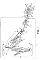
- FIG. 12 schematically shows principal part of a conventional EUV reduction projection exposure apparatus 1000.
- 1001 denotes an EUV light emission point
- 1002 denotes EUV light
- 1003 denotes a filter
- 1004 denotes a first rotational paraboloid mirror
- 1005 denotes a reflection-type or reflection integrator
- 1006 denotes a second rotational paraboloid mirror
- 1007 denotes a reflection mask
- 1008 denotes plural mirrors that constitute a projection optical system
- 1009 denotes a wafer
- 1010 denotes a mask stage
- 1011 denotes a wafer stage
- 1012 denotes an arc aperture
- 1013 denotes a laser light source
- 1014 denotes a laser condensing optical system
- 1017 denotes a vacuum container.
- FIG. 14 is a plane view showing a relationship between an illuminated area 1015 on the mask 1007 and an arc area 1016 to be exposed.
- the exposure apparatus 1000 thus includes a light source section 1013, 1014 that generates the EUV light, an illumination optical system (i.e., the first rotational paraboloid mirror 1004, the reflection integrator 1005 and the second rotational paraboloid mirror 1006), the reflection mask 1007, the projection optical system 1008, the wafer 1009, the mask mounted stage 1010, the wafer mounted stage 1011, an alignment mechanism (not shown) for precise alignment between mask and wafer positions, the vacuum container 1017 that maintains vacuum of the entire optical system vacuum for reduced attenuations of the EUV light, and an exhaust apparatus (not shown).
- an illumination optical system i.e., the first rotational paraboloid mirror 1004, the reflection integrator 1005 and the second rotational paraboloid mirror 1006
- the reflection mask 1007 i.e., the first rotational paraboloid mirror 1004, the reflection integrator 1005 and the second rotational paraboloid mirror 1006
- the reflection mask 1007 i.e., the first rotational paraboloid mirror 1004, the reflection integrator 100
- the illumination optical system uses the first rotational paraboloid mirror 1004 to condense the EUV light 1002 from the emission point 1001 into the reflection integrator 1005 so as to form secondary light sources, and uses the second rotational paraboloid mirror 1006 to superimpose and condense the EUV light from these secondary light sources so as to uniformly illuminate the mask 1007.
- the reflection mask 1007 forms a pattern to be transferred, using a non-reflected part made of an EUV absorber on a multilayer mirror.
- the projection optical system 1008 images, on the wafer 1009, the EUV light that has information of a circuit pattern reflected by the reflection mask 1007.
- the projection optical system 1008 is configured to have excellent imaging performance in an off-axis, thin arc area (i.e. , apart from an optical-axis center).
- the aperture 1012 with the arc opening just prior to the wafer 1009 enables exposure to use only this thin arc area.
- the exposure scans the reflection mask 1007 and the wafer 1009 simultaneously and transfers a rectangular shot on the entire surface of the mask.
- the projection optical system 1008 is comprised of plural multilayer mirrors, and configured to project a reduced size of pattern on the mask 1007 onto the wafer 1009 surface.
- the projection optical system 1008 typically forms an image-side telecentric system, and usually provides an object side (or the reflection mask side) with a non-telecentric structure so as to avoid physical interference with the illumination light incident upon the reflection mask 1007.
- the laser condensing optical system 1014 condenses a laser beam from the laser light source 1013 onto a target (not shown) at the emission point 1001, generating a high-temperature plasma light source 1001.
- the EUV light 1002 thermally radiated from this plasma light source is reflected on the first rotational paraboloid mirror 1004 and turns into parallel EUV light. This light is reflected on the reflection integrator 1005 and forms a multiplicity of secondary light sources.
- the EUV light from these secondary light sources is reflected on the second rotational paraboloid mirror 1006 and illuminates the reflection mask 1007.
- Distances from the secondary light sources to the second rotational paraboloid mirror 1006 and from the secondary rotational paraboloid mirror 1006 to the reflection mask 1007 are set to be equal to a focal distance of the second rotational paraboloid mirror 1006.
- the projection optical system 1008 is configured to project an image of the secondary light sources onto an entrance pupil surface, and thereby meets the Kohler's illumination conditions.
- the EUV light that illuminates one point on the reflection mask 1007 is superimposed EUV beams emitted from all the secondary light sources.
- the illuminated area 1015 on the mask surface is similar, as shown in FIG. 13, to a plane shape of a concave or convex mirror as an element in the reflection integrator 1005, and it is an approximately rectangular shape that includes the arc shape 1016 to be actually exposed.
- the projection optical system 1008 is configured to project an image of the secondary light sources onto its pupil surface.
- the conventional EUV reduction projection exposure apparatus has been disadvantageous, because the aperture 1012 that defines an illuminated area is provided near the wafer 1009 and should be somewhat apart from the driving wafer during exposure. This separation defocuses the exposure area.
- an exemplary object of the present invention to provide an exposure apparatus, which clarifies an imaging system between an reticle and an aperture for defining an illuminated area, and includes an illumination optical system that has the imaging system.
- an exposure apparatus of one aspect according to the present invention includes an illumination optical system for illuminating a pattern of a reflection mask, by using light from a light source, wherein the illumination optical system includes a field stop that defines an illuminated area on the reflection mask, and has an opening, and an imaging system for directing the light from the opening in the field stop into the reflection mask, the imaging system being a coaxial optical system, and a projection optical system for projecting the pattern on the reflection mask onto a substrate, wherein a principal ray of the imaging system at a side of the reflection mask forming an inclination angle to a common axis of the coaxial optical system, the inclination angle being approximately equal to an angle between a principal ray of the projection optical system at the side of the reflection mask and a normal to a surface of the reflection mask.
- FIG. 1 is a schematic view of an embodiment according to the present invention.
- FIG. 2 is a view of an integrator that receives parallel light.
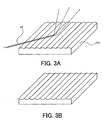
- FIG. 3A is a schematic view of a reflection integrator having plural convex cylindrical surfaces
- FIG. 3B is a schematic view of a reflection integrator having plural concave cylindrical surfaces.
- FIG. 4 is a view of a sectional shape of the integrator.
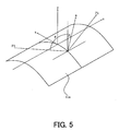
- FIG. 5 is a view for explaining an angular distribution of light reflected on a cylindrical surface.
- FIG. 6 is a view showing an arc area formed by the light reflected on the cylindrical surface.
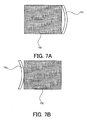
- FIG. 7A is a view in a scan exposure start state
- FIG. 7B is a view in a scan exposure end state.
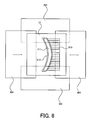
- FIG. 8 is a schematic view of a variable arc slit and a masking blade.
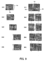
- FIG. 9 is a view showing actions of the masking blade during scan exposure.
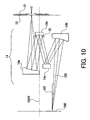
- FIG. 10 is a schematic view of a masking imaging system.
- FIG. 11A is a view showing an aperture stop corresponding to a large ⁇ mode in a normal illumination
- FIG. 11B is a view showing an aperture stop corresponding to a small ⁇ mode in a normal illumination
- FIG. 11C is a view showing an aperture stop corresponding to an annular illumination mode
- FIG. 11D is a view showing an aperture stop corresponding to a quadrupole illumination mode.
- FIG. 12 is a schematic view of a prior art illustration.
- FIG. 13 is a schematic perspective view of a conventional reflection integrator.
- FIG. 14 is a view of a conventional illuminated area and an arc area to be exposed.
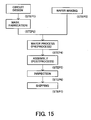
- FIG. 15 is a flowchart for explaining a method for fabricating devices (semiconductor chips such as ICs, LSIs, and the like, LCDs, CCDs, etc.).
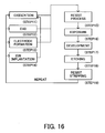
- FIG. 16 is a detailed flowchart for Step 4 of wafer process shown in FIG. 15.
- FIG. 1 is a schematic view of an embodiment according to the present invention.
- 1 denotes an excitation laser beam.
- 2 denotes a plasma emission point.
- 3a denotes a nozzle that injects a liquid drop as a target for plasma generations, and 3b denotes a liquid-drop recovery part for recovering and recycling liquid drops that have not received excitation laser beam.
- 4 denotes a condenser mirror that receives light emitted from the plasma emission point.
- 6a denotes a filter that removes flying particles (or debris) from the plasma
- 6b denotes a wavelength filter that removes light other than the EUV light.
- 7 denotes a pinhole aperture arranged at or near the condensed point of the condenser mirror 4.
- 8 denotes a vacuum container that accommodates the plasma light source. These elements constitute a light source section.
- 5 denotes the EUV light condensed by the mirror 4.
- 9 denotes a connector that connects an exposure apparatus body to a plasma light source section in a vacuum state.
- 10a and 10b are part of a parallelizing optical system that receives the EUV light through the aperture 7, converts it into parallel light, and includes a concave mirror and a convex mirror.
- 11a is an integrator having plural cylindrical mirrors
- 11b and 11c are part of an optical system that includes a rotational paraboloid mirror for condensing the light from the integrator 11a into an arc shape.
- 12, 13 constitute a slit system (or a field stop) wherein 12 denotes a slit that has an arc opening and a partially variable width.
- 13 denotes a masking blade for restricting the illumination light to a desired exposed area, located on a surface conjugate to the reflection mask 16.
- 14 denotes a masking imaging system that images at a desired magnification with respect to the masking blade 13 as the object side and the reflection mask 16 as the image side, and forms an arc illuminated area on the reflection mask.
- 14a, 14b, 14c and 14d, respectively, denote a curved mirror in the masking imaging system 14, and 14e is a plane mirror that reflects light from the imaging system 14 to 14d to reflect the image-side light 14' of the masking imaging system 14 for entry into the reflection mask 16 at a predetermined angle.
- 15 denotes an aperture stop located at a pupil surface in the masking imaging system 14a to 14d.
- 17 denotes a mask stage that holds the reflection mask 16.
- 18 denotes a projection optical system that includes plural mirrors, forms a coaxial optical system, and provides an object side with non-telecentricity and an image side with telecentricity.
- 19 denotes a wafer that applies a photosensitive material.
- 20 denotes a wafer stage that holds the wafer 19
- 21 denotes a vacuum container that maintains the entire optical system in the vacuum atmosphere for reduced attenuation of the EUV light.
- the excitation pulse laser beam 1 irradiates liquid drops to generate the high-temperature plasma from the emission point 2, and the thermal radiation from this plasma generates the EUV light.
- the target may use Xe liquid drops as a target
- the target may use Xe gas injected into a vacuum, a cluster generated from an adiabatic expansion, solidified Xe gas that has been cooled on the metal surface, and a metal tape, such as Cu.
- the EUV light source can use an undulator, or a so-called discharge method, such as Z pinch method, a plasma focus, a capillary discharge, and hollow cathode triggered Z pinch.
- the EUV light irradiated from the plasma emission point 2 is condensed by the condenser mirror 4, such as a rotational spheroid mirror, and taken out as a EUV beam.
- the filter 6a removes flying particles (or debris) that fly ahead directly from the plasma and its vicinity, and the filter 6b removes an unnecessary wavelength component for the EUV exposure, as required.
- the light is condensed into the pinhole aperture 7 provided on a boundary surface between the vacuum container 8 that accommodates the plasma light source, and the vacuum container 21 that accommodates the exposure apparatus body.
- the connector 9 connects the vacuum container 8 that accommodates the light source to the vacuum container 21 that accommodates the exposure apparatus body.
- the EUV light 5 that has passed through the aperture 7 is converted into approximately parallel light 10' by the parallelizing optical system that includes a concave mirror 10a that has an opening at its center, and a convex mirror 10b that has a smaller diameter than the concave mirror 10a.
- the concave mirror 10a has an opening for light reflected by the convex mirror 10b, and its opening is located on the optical axis of the EUV light from the light source.
- These mirrors 10a and 10b have a reflective surface of approximately rotational symmetry with respect to the optical axis of the EUV light from the light source.
- the center axis approximately accords with the optical axis of the EUV light.
- the above condenser mirror 4, and the mirrors 10a and 10b form a reflective multilayer for effectively reflect the EUV light, and become at high temperature during exposure since they absorb the radiant energy from the high-temperature plasma 2. Therefore, they are made of a material with high thermal conductivity, such as metal, and have cooling means (not shown), such as water cooling, for continuous cooling during exposure.
- a reflective surface of each mirror in the optical system forms a reflective multilayer to effectively reflect the EUV light
- the mirror can be made of a material with high thermal conductivity, such as metal, as required.
- the EUV light 10' that has been converted into approximately parallel light enters the integrator 11a that has plural reflective cylindrical mirrors, and the plane mirror 11b and the rotational paraboloid mirror 11c condense, into an arc shape, divergent beams divided by each cylindrical surface, thereby forming an arc illuminated area that has uniform light intensity distribution on the opening in the arc slit 12.
- FIG. 3A is a typical perspective view of the reflection convex cylindrical integrator 11a having plural convex cylindrical surfaces which receives parallel light, and the approximately parallel EUV light 10' enters in the illustrated direction.
- FIG. 3B is a typical perspective view of a reflection concave cylindrical integrator having plural concave cylindrical surfaces that exhibit similar effects to FIG. 3A.
- the integrator 11a in FIG. 1 is a reflection convex cylindrical integrator, as shown in FIG. 3A, but it may be a reflection concave cylindrical integrator shown in FIG. 3B or a combination thereof.
- FIG. 4 is a typical sectional view of the reflection convex cylindrical integrator
- FIG. 5 is a view for explaining reflections of the EUV light on the cylindrical surface of the reflection convex cylindrical integrator
- FIG. 6 is an angular distribution diagram of the EUV light reflected the reflection convex cylindrical integrator.
- reference numeral 11a denotes the reflection convex cylindrical integrator.
- the secondary light source is formed near the integrator surface and the EUV light radiated from this secondary light source has a cone angular distribution. Then the arc illumination is available by reflecting the EUV light on the mirror that has a focal point at a position of this secondary light source, and illuminating the reflection mask or a surface conjugate with the reflection mask.
- this secondary light source exists as a real image outside the reflective surface, whereas when the integrator has a convex cylindrical surface, this secondary light source exits as a virtual image inside the reflective surface.
- the ray vector P2 exists as an arc 601 having a center angle of 4 ⁇ on the xy plane as shown in FIG. 6.
- the secondary light source emits the cone divergent light, which is then reflected on the mirror having the focal distance f and then converted into parallel light.
- the reflected light is a sheet beam having an arc section with a radius f x cos ⁇ and a center angle of 2 ⁇ . Therefore, as shown in FIG. 6, only the arc area 601 is illuminated with a radius of f x cos ⁇ and a center angle of 2 ⁇ on the illuminated surface.
- FIG. 2 a description will be given of the integrator 11a that arranges a multiplicity of cylindrical surfaces in parallel on a large area, and receives the parallel light 10' with a certain beam diameter in a direction shown in FIG. 1.
- 11a is the above integrator
- 11b is a plane mirror
- 11c is a rotational paraboloid mirror
- 12 is a slit having an arc opening.
- the rotational paraboloid mirror 11c is a mirror that is centrically symmetrical around a shaft 201AX, and has a reflective surface that is part of a surface formed by rotating a paraboloid having a focal point 202 around an axis 201AX.
- a distance between the focal point 202 and the mirror effective part's center point 204 is the focal distance f.
- a distance between the point 204 and the arc slit 12 is set to be approximately equal to the focal distance f.
- the rotational paraboloid mirror 11c is arranged so that its rotational axis 201AX is arranged parallel to the reflective surface on or near the reflective surface of the integrator 11a, and aligned with the cylindrical surfaces.
- the plane mirror 11b is located between the effective part's center point 204 and the focal point 202 on the rotational paraboloid mirror 11c, the point 202' that is symmetrical to the focal point 202 with respect to the reflective surface of the mirror 11b can be located approximately at a center position of the reflective surface's effective part on the integrator 11a.
- an optical path length from the position 204 to the position 202' is equal to the focal distance f.
- This arrangement provides the position 202' and the arc slit 12 with a separation by the focal distance f from the rotational paraboloid mirror 11b or a relationship of the Fourier conversion surface. Therefore, the approximately parallel EUV light 10' incident upon the integrator 11a as illustrated is condensed at or near the opening of the arc slit 12.
- the EUV light to the rotational paraboloid mirror 11c has a low incident angle ⁇ of the primary ray between 0° and 45°, more specifically, 20°.
- the arc illuminated area maintains uniform light intensity since the multiple cylindrical surfaces on the integrator 11a superimpose the light. In other words, this can achieve effective and uniform arc illumination.
- the masking blade 13 partially restricts the arc illuminated area formed near the opening in the arc slit 12, and the masking imaging system 14 enlarges or reduces the arc illuminated area at a desired magnification.
- the reflection mask 16 is illuminated with an arc shape by introducing the arc illuminated area at a desired incident angle into the reflection mask 16 held by the mask stage 17.
- the center of curvature of the arc illuminated area accords with the optical axis 18AX of the projection optical system 18.
- the circuit pattern is exposed when the projection optical system 18 projects, onto the wafer 19 that applies a photosensitive material, at a magnification suitable for exposure, the reflected EUV light having circuit pattern information from the reflection mask 16 that has been illuminated in an arc shape.
- the above wafer is fixed on the wafer stage 20, which serves to provide back and forth and up and down parallel movements on the paper surface under control of distance measuring equipment, such as a laser interferometer (not shown).
- the scan exposure over the entire surface requires, for example, the reflection mask 16 to be scanned at a speed v in a direction parallel to the paper surface and the wafer 19 to be simultaneously synchronously scanned at a speed v / M in the direction parallel to the paper, where M is a magnification of the projection optical system 18.
- the projection optical system 18 is comprised of plural multilayer reflective mirrors, and provided with excellent imaging performance in an off-axis, thin arc area.
- the projection optical system 18 is configured to project a reduced size of the pattern on the mask 16 onto the wafer 19 surface, and form an image-side (or wafer-side) telecentric system.
- the projection optical system 1008 provides an object side (or the reflection mask side) with a non-telecentric structure so as to avoid physical interference with the illumination light incident upon the reflection mask 16, and the instant embodiment inclines the image-side principal ray, for example, by about 6° relative to the normal direction of the mask 16.
- FIGS. 7A and 7B show scan exposure start and end states on the wafer surface, respectively.
- 701 denotes an arc illuminated area on the wafer surface.
- 702 denotes an exposed area as an object to be exposed.
- the exposure area 702 moves from left to right on the paper when the wafer stage is driven.
- the arc illuminated area 701 is configured to relatively scan the exposed area 702.
- the masking blade works so that the arc illuminated area 701 is prevented from illuminating part except for the exposure area 702 at the exposure start and exposure end. This will be described in the operation of the masking blade.
- the above is applicable to scan exposure in a relatively reverse direction to the scanned direction in this embodiment.
- 810 denotes a multiple movable edges for partially changing a slit width 811 in the arc slit 12.
- 811 denotes a slit opening for forming the arc illuminated area.
- 812 denotes an arc illuminated area formed by the above integrator 11a and mirror system 11b and 11c, and this illuminated area defines light that passes through the slit opening 811.
- the uneven exposure occurs if there is uneven light intensity in the arc slit when the scan exposure transfers a reduced size of the circuit pattern in the reflection mask 16 onto the wafer 19.
- One solution for this problem uses a drive system (not shown) to move the movable edges 810 to narrow only the slit width that provides relatively strong light intensity in the arc slit, and to reduce the light amount for the scan exposure by a desired amount. As a result, exposure with uniform intensity is available on the entire exposed surface as a result of accumulation.
- the masking blade 13 includes four light-shielding plates 801, 802, 803 and 804, the upper and lower light-shielding plates 803 and 804 shield light at both ends of the arc illuminated area 812 in the arc slit opening 812, and define a longitudinal width (or a scan width) of the exposed area 702 shown in FIG. 7A.
- the light-shielding plates 801 and 802 define a lateral width (or a scan length) in the exposed area 702 by moving in a lateral direction and opening and closing an aperture from the exposure start to the exposure end for one shot in the scan exposure, as described in detail below, with reference to FIG. 9.
- (A1) to (A5) time-sequentially represent scan exposure from a start to an end, while (B1) to (B5) show actions of light-shielding plates 801 and 802 in the masking blade 13 at states (A1) to (A5).
- the exposure is about to start at the state (A1), and the light-shielding plate 802 starts to move to the right at the state (B1) to open the aperture.
- the arc illuminated area 701 is light-shielded in this state, and not actually illuminated although illustrated.
- the scan exposure starts as shown in (A2)
- the light-shielding plate 802 moves as shown in the state (B2) so as to light-shield a projection the arc illuminated area 701 from the exposure area 702.
- the arc illuminated area 701 moves within the exposed area 702 for scan exposure
- the light-shielding plate 802 moves to the right as shown in (B3) to completely open the slit opening 811.
- the light-shielding plate 801 moves to the right so as to light-shield a projection of the arc illuminated area 701 from the exposed area 702.
- the light-shielding plate 801 moves and completely shields the slit opening 811. The above series of actions provides the scan exposure for a desired exposed area.
- the masking imaging system 14 is an imaging optical system that uses the above masking blade 13 as an image surface, and the reflection mask 16 (at a position 102 in the figure) as an image surface, and includes reflective multilayer mirrors.
- This imaging system is a coaxial optical system that serves to image and form an arc illuminated area suitable for the projection optical system 18 by applying a desired magnification to the object-side arc area that arranges the common axis (or optical axis) 10A nearly at a center.
- 14a, 14b, 14c and 14d are concave or convex spherical or aspheric mirrors that use the center axis 10AX for rotational symmetry, and are concave, concave, convex and concave from 14a in the instant embodiment.
- the pupil surface in the masking imaging system 14 is located on or near the reflective surface of the mirror 14b, at which the aperture stop 15 is located.
- the aperture stop 15 changes its opening pattern to change a convergent angle (or a so-called coherence factor ⁇ ) of the illumination light at the reflection mask side, or to provide modified illumination, as described in detail below:
- the incident light condenses into the image surface 102 through the above four mirrors and aperture stop 15.
- the image side has a non-telecentric structure, and an incident angle 101 upon the image surface 102 of the principal ray 103 (or an angle between the principal ray 103 and the rotationally symmetrical axis 10AX) is set to be approximately equal to the inclination angle of the object-side principal ray of the projection optical system 18 to the mask-surface normal.
- an angle between the mask-side principal ray of the imaging system 14a to 14d and the rotationally symmetrical axis 10AX, corresponding to each position on the reflection mask's illuminated area is set to be approximately equal to an angle between the mask-side principal ray of the projection optical system and the normal to the mask surface.
- the instant embodiment sets the incident angle 101 to be about 6°, equal to the angle between the mask-side principal ray of the projection optical system 18 and the normal to the mask surface. Since the optical axis 18X of the projection optical system is parallel to the normal to the mask surface, an angle between the optical axis 18X of the projection optical system and the mask-side principal ray of the projection optical system 18.
- the angle between the mask-side principal ray of the imaging system and the optical axis of the imaging system is approximately equal to the angle between the angle between the mask-side principal ray of the projection optical system and the normal to the mask surface.
- the imaging surface properly corrects defocus at the image side, and the spot diameter on the image surface is designed to be 5 mm or smaller, preferably 1 mm or smaller.
- the plane mirror 14e reflects the image-side light 14' of the masking imaging system 14 shown in FIG. 1 and angles it toward the reflection mask 16, an orientation of an arc illuminated area formed by the light 14' is reversed and the arc's center accords with an intersection between the center axis 18AX of the projection system 18 and the reflection mask.
- the above incident angle 101 enables the principal ray of the light 14' to approximately accord with the principal ray of the object-side light 18' of the projection optical system 18 with respect to a reflective surface on the reflection mask.
- FIGS. 11A to 11D are views of exemplary opening shapes of the aperture stop 15.
- a stop in FIG. 11A has a circular opening and corresponds to a large ⁇ mode in a normal illumination.
- a stop in FIG. 11B has a circular opening smaller than the stop in FIG. 11A and corresponds to a small ⁇ mode in a normal illumination.
- a stop in FIG. 11C has an annular opening and corresponds to the annular illumination mode.
- a stop in FIG. 11D has four openings and corresponds to the quadrupole illumination mode.
- FIG. 15 is a manufacture flow for explaining a fabrication of devices (i.e. , semiconductor chips such as IC and LSI, LCDs, CCDs, etc.).
- a fabrication of a semiconductor chip As an example.
- Step 1 circuit design
- Step 2 mask fabrication
- Step 3 wafer making
- Step 4 wafer process
- a pretreatment forms actual circuitry on the wafer through photolithography using the mask and wafer.
- Step 5 (assembly), which is also referred to as a posttreatment, forms into a semiconductor chip the wafer formed in Step 4 and includes an assembly step ( e.g., dicing, bonding), a packaging step (chip sealing), and the like.
- Step 6 (inspection) performs various tests for the semiconductor device made in Step 5, such as a validity test and a durability test. Through these steps, a semiconductor device is finished and shipped (Step 7).
- FIG. 16 is a detailed flow of the above wafer process.
- Step 11 oxidation
- Step 12 CVD
- Step 13 electrode formation
- Step 14 ion implantation
- Step 15 resist process
- Step 16 exposure
- Step 17 development
- Step 18 etching
- Step 19 resist stripping
- the present invention is applicable to another illumination optical system that uses different light, for example, light in an EUV or E-ray region with a wavelength between 10 nm and 200 nm.
- No glass material is applicable as a lens for light with a wavelength between 20 and 50 nm, and the optical system should include mirrors only. Therefore, the present invention is effectively applicable to the illumination optical system that uses this region.
- An exposure apparatus includes an illumination optical system for illuminating a reflection mask that forms a pattern, by using light from a light source, wherein the illumination optical system includes a field stop that defines an illuminated area on the reflection mask, and has an opening, and an imaging system for introducing the light from the opening in the field stop into the reflection mask, the imaging system being a coaxial optical system, wherein a principal ray of the imaging system at a side of the reflection mask forming an inclination angle to a common axis of the coaxial optical system, the inclination angle being approximately equal to an angle between a principal ray of the projection optical system at the side of the reflection mask and a normal to a surface of the reflection mask.
Landscapes
- Physics & Mathematics (AREA)
- General Physics & Mathematics (AREA)
- Exposure And Positioning Against Photoresist Photosensitive Materials (AREA)
- Exposure Of Semiconductors, Excluding Electron Or Ion Beam Exposure (AREA)
Abstract
Description
- The present invention relates generally to an exposure apparatus, and more particularly to an exposure apparatus that uses a light source in an extreme ultraviolet ("EUV") or X-ray region with a wavelength between 10 nm and 200 nm to expose an object, such as a single crystal substrate for a semiconductor wafer, and a glass plate for a liquid crystal display ("LCD").
- A reduction projection exposure method that uses, for example, EUV light or X-ray have been proposed as one of methods for manufacturing semiconductor circuit devices having a fine pattern (see, for example, Japanese Patent Application Publication No. 10-70058 (or its U.S. counterpart, U.S. Patent No. 6, 504, 896B1), Japanese Patent Application Publication No. 2003-045774 (or its U.S. counterpart, U.S. Patent Application Publication No. 2003031017A1), and Japanese Patent Application Publication No. 2003-045784 (or its U.S. counterpart, U.S. Patent Application Publication No. 2003031017A1).
- This method uses the EUV light to illuminate a mask (or a reticle) that forms a circuit pattern, and projects a reduced size of the pattern on the mask, onto a wafer surface, and to expose photoresist on the wafer surface for pattern transfer.
- FIG. 12 schematically shows principal part of a conventional EUV reduction
projection exposure apparatus 1000. In FIG. 12, 1001 denotes an EUV light emission point, 1002 denotes EUV light, 1003 denotes a filter, 1004 denotes a first rotational paraboloid mirror, 1005 denotes a reflection-type or reflection integrator, 1006 denotes a second rotational paraboloid mirror, 1007 denotes a reflection mask, 1008 denotes plural mirrors that constitute a projection optical system, 1009 denotes a wafer, 1010 denotes a mask stage, 1011 denotes a wafer stage, 1012 denotes an arc aperture, 1013 denotes a laser light source, 1014 denotes a laser condensing optical system, and 1017 denotes a vacuum container. FIG. 14 is a plane view showing a relationship between anilluminated area 1015 on themask 1007 and anarc area 1016 to be exposed. - The
exposure apparatus 1000 thus includes alight source section rotational paraboloid mirror 1004, thereflection integrator 1005 and the second rotational paraboloid mirror 1006), thereflection mask 1007, the projectionoptical system 1008, the wafer 1009, the mask mountedstage 1010, the wafer mountedstage 1011, an alignment mechanism (not shown) for precise alignment between mask and wafer positions, thevacuum container 1017 that maintains vacuum of the entire optical system vacuum for reduced attenuations of the EUV light, and an exhaust apparatus (not shown). - The illumination optical system uses the first
rotational paraboloid mirror 1004 to condense theEUV light 1002 from theemission point 1001 into thereflection integrator 1005 so as to form secondary light sources, and uses the secondrotational paraboloid mirror 1006 to superimpose and condense the EUV light from these secondary light sources so as to uniformly illuminate themask 1007. - The
reflection mask 1007 forms a pattern to be transferred, using a non-reflected part made of an EUV absorber on a multilayer mirror. The projectionoptical system 1008 images, on the wafer 1009, the EUV light that has information of a circuit pattern reflected by thereflection mask 1007. - The projection
optical system 1008 is configured to have excellent imaging performance in an off-axis, thin arc area (i.e., apart from an optical-axis center). Theaperture 1012 with the arc opening just prior to the wafer 1009 enables exposure to use only this thin arc area. The exposure scans thereflection mask 1007 and the wafer 1009 simultaneously and transfers a rectangular shot on the entire surface of the mask. - The projection
optical system 1008 is comprised of plural multilayer mirrors, and configured to project a reduced size of pattern on themask 1007 onto the wafer 1009 surface. The projectionoptical system 1008 typically forms an image-side telecentric system, and usually provides an object side (or the reflection mask side) with a non-telecentric structure so as to avoid physical interference with the illumination light incident upon thereflection mask 1007. - The laser condensing
optical system 1014 condenses a laser beam from thelaser light source 1013 onto a target (not shown) at theemission point 1001, generating a high-temperatureplasma light source 1001. The EUVlight 1002 thermally radiated from this plasma light source is reflected on the firstrotational paraboloid mirror 1004 and turns into parallel EUV light. This light is reflected on thereflection integrator 1005 and forms a multiplicity of secondary light sources. - The EUV light from these secondary light sources is reflected on the second
rotational paraboloid mirror 1006 and illuminates thereflection mask 1007. Distances from the secondary light sources to the secondrotational paraboloid mirror 1006 and from the secondaryrotational paraboloid mirror 1006 to thereflection mask 1007 are set to be equal to a focal distance of the secondrotational paraboloid mirror 1006. - Since a focal point of the second
rotational paraboloid mirror 1006 is located at positions of the second light sources, the EUV light emitted from the secondary light sources irradiates as parallel light thereflection mask 1007. The projectionoptical system 1008 is configured to project an image of the secondary light sources onto an entrance pupil surface, and thereby meets the Kohler's illumination conditions. The EUV light that illuminates one point on thereflection mask 1007 is superimposed EUV beams emitted from all the secondary light sources. - The
illuminated area 1015 on the mask surface is similar, as shown in FIG. 13, to a plane shape of a concave or convex mirror as an element in thereflection integrator 1005, and it is an approximately rectangular shape that includes thearc shape 1016 to be actually exposed. The projectionoptical system 1008 is configured to project an image of the secondary light sources onto its pupil surface. - However, the conventional EUV reduction projection exposure apparatus has been disadvantageous, because the
aperture 1012 that defines an illuminated area is provided near the wafer 1009 and should be somewhat apart from the driving wafer during exposure. This separation defocuses the exposure area. - It is conceivable to provide a similar aperture near the
reflection mask 1007, but the same problem occurs. The problem would be serious because the similar aperture should be located near thereflection mask 1007 so that it does not shield necessary light incident upon and exiting from the reflection mask. - It is also conceivable to provide an imaging system between a reticle and an aperture for defining the illuminated area, its detailed structure has not been conventionally clarified.
- Accordingly, with the foregoing conventional problems in mind, it is an exemplary object of the present invention to provide an exposure apparatus, which clarifies an imaging system between an reticle and an aperture for defining an illuminated area, and includes an illumination optical system that has the imaging system.
- In order to achieve the above object, an exposure apparatus of one aspect according to the present invention includes an illumination optical system for illuminating a pattern of a reflection mask, by using light from a light source, wherein the illumination optical system includes a field stop that defines an illuminated area on the reflection mask, and has an opening, and an imaging system for directing the light from the opening in the field stop into the reflection mask, the imaging system being a coaxial optical system, and a projection optical system for projecting the pattern on the reflection mask onto a substrate, wherein a principal ray of the imaging system at a side of the reflection mask forming an inclination angle to a common axis of the coaxial optical system, the inclination angle being approximately equal to an angle between a principal ray of the projection optical system at the side of the reflection mask and a normal to a surface of the reflection mask.
- Other features and advantages of the present invention will be apparent from the following description taken in conjunction with the accompanying drawings, in which like reference characters designate the same or similar parts throughout the figures thereof.
- The accompanying drawings, which are incorporated in and constitute a part of the specification, illustrate embodiments of the invention and, together with the description, serve to explain the principles of the invention.
- FIG. 1 is a schematic view of an embodiment according to the present invention.
- FIG. 2 is a view of an integrator that receives parallel light.
- FIG. 3A is a schematic view of a reflection integrator having plural convex cylindrical surfaces, and FIG. 3B is a schematic view of a reflection integrator having plural concave cylindrical surfaces.
- FIG. 4 is a view of a sectional shape of the integrator.
- FIG. 5 is a view for explaining an angular distribution of light reflected on a cylindrical surface.
- FIG. 6 is a view showing an arc area formed by the light reflected on the cylindrical surface.
- FIG. 7A is a view in a scan exposure start state, and FIG. 7B is a view in a scan exposure end state.
- FIG. 8 is a schematic view of a variable arc slit and a masking blade.
- FIG. 9 is a view showing actions of the masking blade during scan exposure.
- FIG. 10 is a schematic view of a masking imaging system.
- FIG. 11A is a view showing an aperture stop corresponding to a large σ mode in a normal illumination, FIG. 11B is a view showing an aperture stop corresponding to a small σ mode in a normal illumination, FIG. 11C is a view showing an aperture stop corresponding to an annular illumination mode, and FIG. 11D is a view showing an aperture stop corresponding to a quadrupole illumination mode.
- FIG. 12 is a schematic view of a prior art illustration.
- FIG. 13 is a schematic perspective view of a conventional reflection integrator.
- FIG. 14 is a view of a conventional illuminated area and an arc area to be exposed.
- FIG. 15 is a flowchart for explaining a method for fabricating devices (semiconductor chips such as ICs, LSIs, and the like, LCDs, CCDs, etc.).
- FIG. 16 is a detailed flowchart for Step 4 of wafer process shown in FIG. 15.
- Preferred embodiments of the present invention will now be described in detail in accordance with the accompanying drawings.
- FIG. 1 is a schematic view of an embodiment according to the present invention. As illustrated, 1 denotes an excitation laser beam. 2 denotes a plasma emission point. 3a denotes a nozzle that injects a liquid drop as a target for plasma generations, and 3b denotes a liquid-drop recovery part for recovering and recycling liquid drops that have not received excitation laser beam. 4 denotes a condenser mirror that receives light emitted from the plasma emission point. 6a denotes a filter that removes flying particles (or debris) from the plasma, and 6b denotes a wavelength filter that removes light other than the EUV light. 7 denotes a pinhole aperture arranged at or near the condensed point of the condenser mirror 4. 8 denotes a vacuum container that accommodates the plasma light source. These elements constitute a light source section. 5 denotes the EUV light condensed by the mirror 4. 9 denotes a connector that connects an exposure apparatus body to a plasma light source section in a vacuum state.
- 10a and 10b are part of a parallelizing optical system that receives the EUV light through the aperture 7, converts it into parallel light, and includes a concave mirror and a convex mirror. 11a is an integrator having plural cylindrical mirrors, and 11b and 11c are part of an optical system that includes a rotational paraboloid mirror for condensing the light from the integrator 11a into an arc shape. 12, 13 constitute a slit system (or a field stop) wherein 12 denotes a slit that has an arc opening and a partially variable width. 13 denotes a masking blade for restricting the illumination light to a desired exposed area, located on a surface conjugate to the
reflection mask 16. 14 denotes a masking imaging system that images at a desired magnification with respect to themasking blade 13 as the object side and thereflection mask 16 as the image side, and forms an arc illuminated area on the reflection mask. 14a, 14b, 14c and 14d, respectively, denote a curved mirror in the maskingimaging system imaging system 14 to 14d to reflect the image-side light 14' of the maskingimaging system 14 for entry into thereflection mask 16 at a predetermined angle. 15 denotes an aperture stop located at a pupil surface in the maskingimaging system 14a to 14d. These elements constitute an illumination optical system for illuminating thereflection mask 16 with light from the light source section. - 17 denotes a mask stage that holds the
reflection mask 16. 18 denotes a projection optical system that includes plural mirrors, forms a coaxial optical system, and provides an object side with non-telecentricity and an image side with telecentricity. 19 denotes a wafer that applies a photosensitive material. 20 denotes a wafer stage that holds thewafer - The high power excitation
pulse laser beam 1, emitted from the excitation laser part that includes an excitation laser light source and condenser optical system (not shown), is configured to condense at a position of the emission point 2, and forms a plasma light source section. The liquid drop as the target of this laser plasma light source, such as Xe, is configured to be continuously injected at regular time intervals from thenozzle 3a, and pass the condensed point 2. When the thus-injected liquid drop is located at the position of the element 2, the excitationpulse laser beam 1 irradiates liquid drops to generate the high-temperature plasma from the emission point 2, and the thermal radiation from this plasma generates the EUV light. - While the instant embodiment uses Xe liquid drops as a target, the target may use Xe gas injected into a vacuum, a cluster generated from an adiabatic expansion, solidified Xe gas that has been cooled on the metal surface, and a metal tape, such as Cu. Alternatively, the EUV light source can use an undulator, or a so-called discharge method, such as Z pinch method, a plasma focus, a capillary discharge, and hollow cathode triggered Z pinch.
- The EUV light irradiated from the plasma emission point 2 is condensed by the condenser mirror 4, such as a rotational spheroid mirror, and taken out as a EUV beam. The
filter 6a removes flying particles (or debris) that fly ahead directly from the plasma and its vicinity, and thefilter 6b removes an unnecessary wavelength component for the EUV exposure, as required. Then, the light is condensed into the pinhole aperture 7 provided on a boundary surface between thevacuum container 8 that accommodates the plasma light source, and thevacuum container 21 that accommodates the exposure apparatus body. The connector 9 connects thevacuum container 8 that accommodates the light source to thevacuum container 21 that accommodates the exposure apparatus body. - The EUV light 5 that has passed through the aperture 7 is converted into approximately parallel light 10' by the parallelizing optical system that includes a
concave mirror 10a that has an opening at its center, and aconvex mirror 10b that has a smaller diameter than theconcave mirror 10a. Here, theconcave mirror 10a has an opening for light reflected by theconvex mirror 10b, and its opening is located on the optical axis of the EUV light from the light source. Thesemirrors - The above condenser mirror 4, and the
mirrors - Although not described specifically, a reflective surface of each mirror in the optical system forms a reflective multilayer to effectively reflect the EUV light, and the mirror can be made of a material with high thermal conductivity, such as metal, as required.
- The EUV light 10' that has been converted into approximately parallel light enters the integrator 11a that has plural reflective cylindrical mirrors, and the
plane mirror 11b and therotational paraboloid mirror 11c condense, into an arc shape, divergent beams divided by each cylindrical surface, thereby forming an arc illuminated area that has uniform light intensity distribution on the opening in the arc slit 12. - A detailed description will now be given of how the integrator 11a uniformly illuminates the arc area, with reference to another figure.
- FIG. 3A is a typical perspective view of the reflection convex cylindrical integrator 11a having plural convex cylindrical surfaces which receives parallel light, and the approximately parallel EUV light 10' enters in the illustrated direction. FIG. 3B is a typical perspective view of a reflection concave cylindrical integrator having plural concave cylindrical surfaces that exhibit similar effects to FIG. 3A. The integrator 11a in FIG. 1 is a reflection convex cylindrical integrator, as shown in FIG. 3A, but it may be a reflection concave cylindrical integrator shown in FIG. 3B or a combination thereof.
- FIG. 4 is a typical sectional view of the reflection convex cylindrical integrator, FIG. 5 is a view for explaining reflections of the EUV light on the cylindrical surface of the reflection convex cylindrical integrator, and FIG. 6 is an angular distribution diagram of the EUV light reflected the reflection convex cylindrical integrator. In each figure, reference numeral 11a denotes the reflection convex cylindrical integrator.
- As shown in FIG. 3A, when approximately parallel EUV light 11 is incident upon the integrator 11a having plural cylindrical surfaces, the secondary light source is formed near the integrator surface and the EUV light radiated from this secondary light source has a cone angular distribution. Then the arc illumination is available by reflecting the EUV light on the mirror that has a focal point at a position of this secondary light source, and illuminating the reflection mask or a surface conjugate with the reflection mask.
- In order to explain operations of the reflection integrator having plural cylindrical surfaces, a description will now be given of a behavior of the reflected light when the parallel light is incident upon one cylindrical mirror with reference to FIG. 5. It is now supposed that parallel light is incident upon one cylindrical surface at an angle e to a surface perpendicular to the center axis.
- When a ray vector of the incident parallel light is defined as P1 = (0, -cos, sin), and a normal vector on the cylindrical reflective surface is defined as n = (-sinα, cosα, 0), the ray vector of the reflected light becomes P2 = (-cos x sin2α, cos x cos2α, sin). The plotted ray vector of the reflected light in a phase space forms a circle with a radius of cos on an xy plane, as shown in FIG. 6. Therefore, the reflected light becomes cone divergent light, and the secondary light source is located on a vertex of this cone surface. When the integrator 11a has a concave cylindrical surface, this secondary light source exists as a real image outside the reflective surface, whereas when the integrator has a convex cylindrical surface, this secondary light source exits as a virtual image inside the reflective surface. As shown in FIG. 4, when the reflective surface is limited to part of the cylindrical surface and has a center angle of 2Φ, the ray vector P2 exists as an
arc 601 having a center angle of 4Φ on the xy plane as shown in FIG. 6. - Then, suppose a rotational paraboloid mirror having a focal distance f and a focal point at the secondary light source's position that is formed as a result of parallel light incident upon the above cylindrical mirror, and an illuminated surface located apart from this mirror by the distance f. The secondary light source emits the cone divergent light, which is then reflected on the mirror having the focal distance f and then converted into parallel light. The reflected light is a sheet beam having an arc section with a radius f x cos and a center angle of 2Φ. Therefore, as shown in FIG. 6, only the
arc area 601 is illuminated with a radius of f x cos and a center angle of 2Φ on the illuminated surface. - The foregoing description refers to one cylindrical mirror. Referring now to FIG. 2, a description will be given of the integrator 11a that arranges a multiplicity of cylindrical surfaces in parallel on a large area, and receives the parallel light 10' with a certain beam diameter in a direction shown in FIG. 1.
- In FIG. 2, 11a is the above integrator, 11b is a plane mirror, 11c is a rotational paraboloid mirror, and 12 is a slit having an arc opening. The
rotational paraboloid mirror 11c is a mirror that is centrically symmetrical around a shaft 201AX, and has a reflective surface that is part of a surface formed by rotating a paraboloid having afocal point 202 around an axis 201AX. A distance between thefocal point 202 and the mirror effective part'scenter point 204 is the focal distance f. A distance between thepoint 204 and the arc slit 12 is set to be approximately equal to the focal distance f. - The
rotational paraboloid mirror 11c is arranged so that its rotational axis 201AX is arranged parallel to the reflective surface on or near the reflective surface of the integrator 11a, and aligned with the cylindrical surfaces. As illustrated, theplane mirror 11b is located between the effective part'scenter point 204 and thefocal point 202 on therotational paraboloid mirror 11c, the point 202' that is symmetrical to thefocal point 202 with respect to the reflective surface of themirror 11b can be located approximately at a center position of the reflective surface's effective part on the integrator 11a. In other words, an optical path length from theposition 204 to the position 202' is equal to the focal distance f. - This arrangement provides the position 202' and the arc slit 12 with a separation by the focal distance f from the
rotational paraboloid mirror 11b or a relationship of the Fourier conversion surface. Therefore, the approximately parallel EUV light 10' incident upon the integrator 11a as illustrated is condensed at or near the opening of the arc slit 12. - The EUV light to the
rotational paraboloid mirror 11c has a low incident angle ζ of the primary ray between 0° and 45°, more specifically, 20°. Thereby, the defocus amount reduces when light is condensed in the arc slit 12 and condensing efficiency improves near the arc opening rather than the high incident angle. Thereby, the optical loss due to shielding reduces, and the illumination system's efficiency improves. - Since the light reflected on the mirror that arranges plural cylindrical surfaces in parallel has the same angular distribution as the above, the arc area is illuminated with a radius f x cosε near the arc slit 12, where e is a light incident angle to the integrator 11a. Since the light incident upon one point near the arc slit 12 results from the entire illuminated area that arranges plural cylindrical surfaces in parallel, the angular range ϒ, i.e., condensing NA, becomes ϒ = D / f, where D is a beam diameter of the approximately parallel EUV light 10'.
- In this case, the arc illuminated area maintains uniform light intensity since the multiple cylindrical surfaces on the integrator 11a superimpose the light. In other words, this can achieve effective and uniform arc illumination.
- Turning back to FIG. 1, a description will be given of the exposure apparatus of the instant embodiment. As illustrated, the
masking blade 13 partially restricts the arc illuminated area formed near the opening in the arc slit 12, and the maskingimaging system 14 enlarges or reduces the arc illuminated area at a desired magnification. As a consequence, thereflection mask 16 is illuminated with an arc shape by introducing the arc illuminated area at a desired incident angle into thereflection mask 16 held by themask stage 17. The center of curvature of the arc illuminated area accords with the optical axis 18AX of the projectionoptical system 18. - The circuit pattern is exposed when the projection
optical system 18 projects, onto thewafer 19 that applies a photosensitive material, at a magnification suitable for exposure, the reflected EUV light having circuit pattern information from thereflection mask 16 that has been illuminated in an arc shape. - The above wafer is fixed on the
wafer stage 20, which serves to provide back and forth and up and down parallel movements on the paper surface under control of distance measuring equipment, such as a laser interferometer (not shown). The scan exposure over the entire surface requires, for example, thereflection mask 16 to be scanned at a speed v in a direction parallel to the paper surface and thewafer 19 to be simultaneously synchronously scanned at a speed v / M in the direction parallel to the paper, where M is a magnification of the projectionoptical system 18. - The projection
optical system 18 is comprised of plural multilayer reflective mirrors, and provided with excellent imaging performance in an off-axis, thin arc area. The projectionoptical system 18 is configured to project a reduced size of the pattern on themask 16 onto thewafer 19 surface, and form an image-side (or wafer-side) telecentric system. The projectionoptical system 1008 provides an object side (or the reflection mask side) with a non-telecentric structure so as to avoid physical interference with the illumination light incident upon thereflection mask 16, and the instant embodiment inclines the image-side principal ray, for example, by about 6° relative to the normal direction of themask 16. - A detailed description will now be given of (1) scan exposure using the arc illumination, (2) a method of correcting uneven exposure by using the arc slit 12, (3) operations of the
masking blade 13 during the scan exposure, and (4) a structure of a masking imaging system in this order. - FIGS. 7A and 7B show scan exposure start and end states on the wafer surface, respectively. As illustrated, 701 denotes an arc illuminated area on the wafer surface. 702 denotes an exposed area as an object to be exposed. In this figure, the
exposure area 702 moves from left to right on the paper when the wafer stage is driven. The arc illuminatedarea 701 is configured to relatively scan the exposedarea 702. The masking blade works so that the arc illuminatedarea 701 is prevented from illuminating part except for theexposure area 702 at the exposure start and exposure end. This will be described in the operation of the masking blade. - The above is applicable to scan exposure in a relatively reverse direction to the scanned direction in this embodiment.
- A detailed description will be given of a method of correcting an uneven exposure with the arc slit 12 in the above scan exposure. As illustrated, 810 denotes a multiple movable edges for partially changing a
slit width 811 in the arc slit 12. 811 denotes a slit opening for forming the arc illuminated area. 812 denotes an arc illuminated area formed by the above integrator 11a andmirror system slit opening 811. - The uneven exposure occurs if there is uneven light intensity in the arc slit when the scan exposure transfers a reduced size of the circuit pattern in the
reflection mask 16 onto thewafer 19. One solution for this problem uses a drive system (not shown) to move themovable edges 810 to narrow only the slit width that provides relatively strong light intensity in the arc slit, and to reduce the light amount for the scan exposure by a desired amount. As a result, exposure with uniform intensity is available on the entire exposed surface as a result of accumulation. - The
masking blade 13 includes four light-shieldingplates plates area 812 in the arc slitopening 812, and define a longitudinal width (or a scan width) of the exposedarea 702 shown in FIG. 7A. - The light-shielding
plates area 702 by moving in a lateral direction and opening and closing an aperture from the exposure start to the exposure end for one shot in the scan exposure, as described in detail below, with reference to FIG. 9. - In FIG. 9, (A1) to (A5) time-sequentially represent scan exposure from a start to an end, while (B1) to (B5) show actions of light-shielding
plates masking blade 13 at states (A1) to (A5). - The exposure is about to start at the state (A1), and the light-shielding
plate 802 starts to move to the right at the state (B1) to open the aperture. The arc illuminatedarea 701 is light-shielded in this state, and not actually illuminated although illustrated. When the scan exposure starts as shown in (A2), the light-shieldingplate 802 moves as shown in the state (B2) so as to light-shield a projection the arc illuminatedarea 701 from theexposure area 702. As shown in (B3), the arc illuminatedarea 701 moves within the exposedarea 702 for scan exposure, the light-shieldingplate 802 moves to the right as shown in (B3) to completely open theslit opening 811. When the scan exposure nearly ends as shown in (A4), the light-shieldingplate 801, in turn, moves to the right so as to light-shield a projection of the arc illuminatedarea 701 from the exposedarea 702. When the scan exposure ends as shown in (A5), the light-shieldingplate 801 moves and completely shields theslit opening 811. The above series of actions provides the scan exposure for a desired exposed area. - Next follows a detailed description of the masking
imaging system 14 with reference to FIG. 10. The maskingimaging system 14 is an imaging optical system that uses theabove masking blade 13 as an image surface, and the reflection mask 16 (at aposition 102 in the figure) as an image surface, and includes reflective multilayer mirrors. This imaging system is a coaxial optical system that serves to image and form an arc illuminated area suitable for the projectionoptical system 18 by applying a desired magnification to the object-side arc area that arranges the common axis (or optical axis) 10A nearly at a center. - As illustrated, 14a, 14b, 14c and 14d are concave or convex spherical or aspheric mirrors that use the center axis 10AX for rotational symmetry, and are concave, concave, convex and concave from 14a in the instant embodiment. The pupil surface in the masking
imaging system 14 is located on or near the reflective surface of themirror 14b, at which theaperture stop 15 is located. Theaperture stop 15 changes its opening pattern to change a convergent angle (or a so-called coherence factor σ) of the illumination light at the reflection mask side, or to provide modified illumination, as described in detail below: - The EUV light condensed at a position of the
masking blade 13 arranged near the arc slit 12 enters the maskingimaging system 14 while the principal ray is parallel to or object-side telecentric to the rotationally symmetrical axis 10AX. The incident light condenses into theimage surface 102 through the above four mirrors andaperture stop 15. Notably, the image side has a non-telecentric structure, and anincident angle 101 upon theimage surface 102 of the principal ray 103 (or an angle between theprincipal ray 103 and the rotationally symmetrical axis 10AX) is set to be approximately equal to the inclination angle of the object-side principal ray of the projectionoptical system 18 to the mask-surface normal. In other words, an angle between the mask-side principal ray of theimaging system 14a to 14d and the rotationally symmetrical axis 10AX, corresponding to each position on the reflection mask's illuminated area is set to be approximately equal to an angle between the mask-side principal ray of the projection optical system and the normal to the mask surface. The instant embodiment sets theincident angle 101 to be about 6°, equal to the angle between the mask-side principal ray of the projectionoptical system 18 and the normal to the mask surface. Since the optical axis 18X of the projection optical system is parallel to the normal to the mask surface, an angle between the optical axis 18X of the projection optical system and the mask-side principal ray of the projectionoptical system 18. Therefore, the angle between the mask-side principal ray of the imaging system and the optical axis of the imaging system is approximately equal to the angle between the angle between the mask-side principal ray of the projection optical system and the normal to the mask surface. The imaging surface properly corrects defocus at the image side, and the spot diameter on the image surface is designed to be 5 mm or smaller, preferably 1 mm or smaller. - When the
plane mirror 14e reflects the image-side light 14' of the maskingimaging system 14 shown in FIG. 1 and angles it toward thereflection mask 16, an orientation of an arc illuminated area formed by the light 14' is reversed and the arc's center accords with an intersection between the center axis 18AX of theprojection system 18 and the reflection mask. Theabove incident angle 101 enables the principal ray of the light 14' to approximately accord with the principal ray of the object-side light 18' of the projectionoptical system 18 with respect to a reflective surface on the reflection mask. - A description will now be given of a method for varying a coherent factor σ and for providing a modified illumination, such as annular illumination, by switching the
aperture stop 15 in the maskingimaging system 14. The aperture stop 15 (or a pupil surface in the masking imaging system) and the pupil surface of the projectionoptical system 18 are conjugate with each other. Therefore, an opening pattern or a light transmission pattern in theaperture stop 15 corresponds to a light-source image on the projection optical system's pupil surface or an effective light source distribution. FIGS. 11A to 11D are views of exemplary opening shapes of theaperture stop 15. A stop in FIG. 11A has a circular opening and corresponds to a large σ mode in a normal illumination. A stop in FIG. 11B has a circular opening smaller than the stop in FIG. 11A and corresponds to a small σ mode in a normal illumination. A stop in FIG. 11C has an annular opening and corresponds to the annular illumination mode. A stop in FIG. 11D has four openings and corresponds to the quadrupole illumination mode. - It is possible to switch to a desired opening shape by preparing several opening patterns, for example, on a turret, and by rotating this turret using an aperture stop drive system (not shown). Instead of using the turret, other mechanical methods may be used, such as switching of plural aperture stops that are linearly arranged or use of an iris stop.
- A description will now be given of an embodiment of a device fabricating method using the exposure apparatus of the first embodiment. FIG. 15 is a manufacture flow for explaining a fabrication of devices (i.e., semiconductor chips such as IC and LSI, LCDs, CCDs, etc.). Here, a description will be given of a fabrication of a semiconductor chip as an example. Step 1 (circuit design) designs a semiconductor device circuit. Step 2 (mask fabrication) forms a mask having a designed circuit pattern. Step 3 (wafer making) manufactures a wafer using materials such as silicon. Step 4 (wafer process), which is referred to as a pretreatment, forms actual circuitry on the wafer through photolithography using the mask and wafer. Step 5 (assembly), which is also referred to as a posttreatment, forms into a semiconductor chip the wafer formed in Step 4 and includes an assembly step (e.g., dicing, bonding), a packaging step (chip sealing), and the like. Step 6 (inspection) performs various tests for the semiconductor device made in Step 5, such as a validity test and a durability test. Through these steps, a semiconductor device is finished and shipped (Step 7).
- FIG. 16 is a detailed flow of the above wafer process. Step 11 (oxidation) oxidizes the wafer's surface. Step 12 (CVD) forms an insulating film on the wafer's surface. Step 13 (electrode formation) forms electrodes on the wafer by vapor disposition and the like. Step 14 (ion implantation) implants ion into the wafer. Step 15 (resist process) applies a photosensitive material onto the wafer. Step 16 (exposure) uses the exposure apparatus of the first embodiment to expose a circuit pattern on the mask onto the wafer. Step 17 (development) develops the exposed wafer. Step 18 (etching) etches parts other than a developed resist image. Step 19 (resist stripping) removes disused resist after etching. These steps are repeated, and a circuit pattern is formed on the wafer.
- Use of the manufacture method of the instant embodiment would be able to manufacture highly integrated devices, which have been difficult to be manufactured.
- While the above embodiments describe the illumination system that uses the EUV light of 13.5 nm, the present invention is applicable to another illumination optical system that uses different light, for example, light in an EUV or E-ray region with a wavelength between 10 nm and 200 nm. No glass material is applicable as a lens for light with a wavelength between 20 and 50 nm, and the optical system should include mirrors only. Therefore, the present invention is effectively applicable to the illumination optical system that uses this region.
- As many apparently widely different embodiments of the present invention can be made without departing from the sprit and scope thereof, it is to be understood that the invention is not limited to the specific embodiments thereof except as defined in the claims.
- An exposure apparatus includes an illumination optical system for illuminating a reflection mask that forms a pattern, by using light from a light source, wherein the illumination optical system includes a field stop that defines an illuminated area on the reflection mask, and has an opening, and an imaging system for introducing the light from the opening in the field stop into the reflection mask, the imaging system being a coaxial optical system, wherein a principal ray of the imaging system at a side of the reflection mask forming an inclination angle to a common axis of the coaxial optical system, the inclination angle being approximately equal to an angle between a principal ray of the projection optical system at the side of the reflection mask and a normal to a surface of the reflection mask.
Claims (18)
- An exposure apparatus comprising an illumination optical system for illuminating a pattern of a reflection mask, by using light from a light source, and a projection optical system for projecting the pattern on the reflection mask onto a substrate, characterized in that said illumination optical system includes a field stop that defines an illuminated area on the reflection mask, and has an opening, and an imaging system for directing the light from the opening in the field stop into the reflection mask, the imaging system being a coaxial optical system, wherein a principal ray of the imaging system at a side of the reflection mask forming an inclination angle to a common axis of the coaxial optical system, the inclination angle being approximately equal to an angle between a principal ray of said projection optical system at the side of the reflection mask and a normal to a surface of the reflection mask.
- An exposure apparatus according to claim 1, characterized in that said illumination optical system includes a plane mirror for reflecting light from the imaging system and for introducing the same into the reflection mask.
- An exposure apparatus according to claim 1, characterized in that the principal ray of the imaging system at a side of the field stop is approximately parallel to the common axis.
- An exposure apparatus according to claim 1, characterized in that said illumination optical system has an aperture stop at a pupil surface in the imaging system.
- An exposure apparatus according to claim 4, characterized in that the aperture stop has an opening, and said illumination optical system has a mechanism for changing a size or a shape of the opening in the aperture stop.
- An exposure apparatus according to claim 1, characterized in that the field stop includes a masking blade that includes plural light-shielding plates.
- An exposure apparatus according to claim 1, characterized in that the field stop includes an arc slit that has an arc opening.
- An exposure apparatus according to claim 7, characterized in that the arc opening has a curvature center on the common axis.
- An exposure apparatus according to claim 1, characterized in that the field stop includes:a masking blade that includes plural light-shielding plates; andan arc slit that has an arc opening.
- An exposure apparatus according to claim 1, characterized in that said illumination optical system includes:a reflection integrator for forming plural secondary light sources using the light from the light source; anda mirror system for superimposing light from plural secondary light sources on the field stop and for forming the arc illuminated area, wherein the arc illuminated area has a curvature center on the common axis.
- An exposure apparatus according to claim 1, characterized in that the imaging system includes four mirrors.
- An exposure apparatus according to claim 11, characterized in that first and fourth mirrors in the four mirrors from the field stop have concave reflective surfaces.
- An exposure apparatus according to claim 11, characterized in that a third mirror in the four mirrors from the field stop has a convex reflective surface.
- An exposure apparatus according to claim 11, characterized in that a second mirror in the four mirrors from the field stop has a concave reflective surface.
- An exposure apparatus according to claim 1, characterized in that the imaging system has a pupil surface, and includes a mirror that has a reflective surface at the pupil surface.
- An exposure apparatus according to claim 1, characterized in that the light from the light source has a wavelength of 200 nm or smaller.
- An exposure apparatus according to claim 16, characterized in that the light from the light source has a wavelength between 5 nm and 20 nm.
- A device fabricating method comprising the steps of:exposing an object using an exposure apparatus according to claim 1; anddeveloping the exposed object.
Applications Claiming Priority (2)
| Application Number | Priority Date | Filing Date | Title |
|---|---|---|---|
| JP2003324639 | 2003-09-17 | ||
| JP2003324639A JP4241281B2 (en) | 2003-09-17 | 2003-09-17 | Exposure equipment |
Publications (2)
| Publication Number | Publication Date |
|---|---|
| EP1517339A2 true EP1517339A2 (en) | 2005-03-23 |
| EP1517339A3 EP1517339A3 (en) | 2009-06-10 |
Family
ID=34191311
Family Applications (1)
| Application Number | Title | Priority Date | Filing Date |
|---|---|---|---|
| EP04001822A Withdrawn EP1517339A3 (en) | 2003-09-17 | 2004-01-28 | Illumination optical system and exposure apparatus |
Country Status (5)
| Country | Link |
|---|---|
| US (2) | US7110084B2 (en) |
| EP (1) | EP1517339A3 (en) |
| JP (1) | JP4241281B2 (en) |
| KR (1) | KR100687655B1 (en) |
| TW (1) | TWI267127B (en) |
Families Citing this family (13)
| Publication number | Priority date | Publication date | Assignee | Title |
|---|---|---|---|---|
| JP4241295B2 (en) * | 2003-09-26 | 2009-03-18 | キヤノン株式会社 | Stage equipment |
| JP4458330B2 (en) * | 2003-12-26 | 2010-04-28 | キヤノン株式会社 | Replacing the multilayer mirror of the light source unit |
| JP2005317611A (en) * | 2004-04-27 | 2005-11-10 | Canon Inc | Exposure method and apparatus |
| JP5030944B2 (en) * | 2005-04-26 | 2012-09-19 | カール・ツァイス・エスエムティー・ゲーエムベーハー | Illumination system for microlithographic exposure apparatus |
| CN101218543A (en) * | 2005-06-14 | 2008-07-09 | 皇家飞利浦电子股份有限公司 | Debris suppression system with improved gas distribution |
| WO2007001624A2 (en) * | 2005-06-28 | 2007-01-04 | Microchips, Inc. | Medical and dental implant devices for controlled drug delivery |
| KR100729263B1 (en) * | 2005-07-14 | 2007-06-15 | 삼성전자주식회사 | Substrate exposure apparatus |
| JP4986754B2 (en) * | 2007-07-27 | 2012-07-25 | キヤノン株式会社 | Illumination optical system and exposure apparatus having the same |
| JP2009176838A (en) * | 2008-01-22 | 2009-08-06 | Canon Inc | Immersion exposure apparatus and device manufacturing method |
| DE102008001553B4 (en) * | 2008-05-05 | 2015-04-30 | Carl Zeiss Smt Gmbh | Component for setting a scan-integrated illumination energy in an object plane of a microlithography projection exposure apparatus |
| US8227778B2 (en) * | 2008-05-20 | 2012-07-24 | Komatsu Ltd. | Semiconductor exposure device using extreme ultra violet radiation |
| JP5534910B2 (en) * | 2009-04-23 | 2014-07-02 | ギガフォトン株式会社 | Extreme ultraviolet light source device |
| US12401779B1 (en) * | 2024-04-09 | 2025-08-26 | DISTANCE TECHNOLOGIES Oy | Calibrating optical combiner using structured light |
Family Cites Families (27)
| Publication number | Priority date | Publication date | Assignee | Title |
|---|---|---|---|---|
| US4861148A (en) * | 1986-03-12 | 1989-08-29 | Matsushita Electric Industrial Co., Inc. | Projection optical system for use in precise copy |
| JPS6329930A (en) | 1986-07-23 | 1988-02-08 | Nec Corp | Reduction stepper |
| JP3111476B2 (en) * | 1991-01-08 | 2000-11-20 | 日本電気株式会社 | Illumination optics |
| US5581605A (en) * | 1993-02-10 | 1996-12-03 | Nikon Corporation | Optical element, production method of optical element, optical system, and optical apparatus |
| US5677939A (en) * | 1994-02-23 | 1997-10-14 | Nikon Corporation | Illuminating apparatus |
| JP3371512B2 (en) | 1994-02-23 | 2003-01-27 | 株式会社ニコン | Illumination device and exposure device |
| KR0135834B1 (en) * | 1994-10-28 | 1998-04-24 | 김광호 | Light source with shadow removing double reflector |
| US5737137A (en) * | 1996-04-01 | 1998-04-07 | The Regents Of The University Of California | Critical illumination condenser for x-ray lithography |
| JP3862347B2 (en) * | 1996-04-11 | 2006-12-27 | キヤノン株式会社 | X-ray reduction exposure apparatus and device manufacturing method using the same |
| JP3706691B2 (en) | 1996-08-26 | 2005-10-12 | キヤノン株式会社 | X-ray reduction projection exposure apparatus and semiconductor device manufacturing method using the same |
| EP1039510A4 (en) * | 1997-11-14 | 2003-11-12 | Nikon Corp | Exposure apparatus and method of manufacturing the same, and exposure method |
| JP4238390B2 (en) * | 1998-02-27 | 2009-03-18 | 株式会社ニコン | LIGHTING APPARATUS, EXPOSURE APPARATUS PROVIDED WITH THE ILLUMINATION APPARATUS, AND METHOD FOR MANUFACTURING SEMICONDUCTOR DEVICE USING THE EXPOSURE APPARATUS |
| JPH11345761A (en) * | 1998-05-29 | 1999-12-14 | Nikon Corp | Scanning exposure equipment |
| JP2000091220A (en) * | 1998-09-08 | 2000-03-31 | Nikon Corp | Projection exposure apparatus and projection exposure method |
| JP2000089000A (en) | 1998-09-14 | 2000-03-31 | Nikon Corp | X-ray generator |
| JP2000100685A (en) | 1998-09-17 | 2000-04-07 | Nikon Corp | Exposure apparatus and exposure method using the apparatus |
| DE50014428D1 (en) | 1999-07-30 | 2007-08-02 | Zeiss Carl Smt Ag | Control of the illumination distribution in the exit pupil of an EUV illumination system |
| JP2002023055A (en) * | 2000-07-10 | 2002-01-23 | Nikon Corp | Image forming optical system and exposure apparatus having the image forming optical system |
| JP2003015040A (en) * | 2001-07-04 | 2003-01-15 | Nikon Corp | Projection optical system and exposure apparatus having the projection optical system |
| DE60217771T3 (en) * | 2001-07-27 | 2012-02-09 | Canon K.K. | Exposure system, projection exposure apparatus and method of making an article |
| JP3605053B2 (en) | 2001-07-27 | 2004-12-22 | キヤノン株式会社 | Illumination optical system, exposure apparatus and device manufacturing method |
| JP3605055B2 (en) * | 2001-07-31 | 2004-12-22 | キヤノン株式会社 | Illumination optical system, exposure apparatus and device manufacturing method |
| JP2003227914A (en) * | 2002-01-31 | 2003-08-15 | Canon Inc | Wavefront splitting element for EUV light and phase measuring device having the same |
| JP2003233005A (en) * | 2002-02-07 | 2003-08-22 | Canon Inc | Reflection type projection optical system, exposure apparatus and device manufacturing method |
| JP3720788B2 (en) * | 2002-04-15 | 2005-11-30 | キヤノン株式会社 | Projection exposure apparatus and device manufacturing method |
| US20040080815A1 (en) * | 2002-07-12 | 2004-04-29 | Peter Muys | Lens with optimized heat transfer properties |
| JP2004138926A (en) * | 2002-10-21 | 2004-05-13 | Nikon Corp | Projection optical system and exposure apparatus having the projection optical system |
-
2003
- 2003-09-17 JP JP2003324639A patent/JP4241281B2/en not_active Expired - Fee Related
-
2004
- 2004-01-28 EP EP04001822A patent/EP1517339A3/en not_active Withdrawn
- 2004-01-29 TW TW093102016A patent/TWI267127B/en not_active IP Right Cessation
- 2004-01-30 US US10/769,373 patent/US7110084B2/en not_active Expired - Fee Related
- 2004-01-30 US US10/768,896 patent/US7064806B2/en not_active Expired - Fee Related
- 2004-09-17 KR KR1020040074612A patent/KR100687655B1/en not_active Expired - Fee Related
Non-Patent Citations (1)
| Title |
|---|
| None |
Also Published As
| Publication number | Publication date |
|---|---|
| KR20050028848A (en) | 2005-03-23 |
| US7064806B2 (en) | 2006-06-20 |
| JP2005093693A (en) | 2005-04-07 |
| EP1517339A3 (en) | 2009-06-10 |
| US20050057737A1 (en) | 2005-03-17 |
| TWI267127B (en) | 2006-11-21 |
| JP4241281B2 (en) | 2009-03-18 |
| TW200512805A (en) | 2005-04-01 |
| KR100687655B1 (en) | 2007-02-28 |
| US7110084B2 (en) | 2006-09-19 |
| US20050057738A1 (en) | 2005-03-17 |
Similar Documents
| Publication | Publication Date | Title |
|---|---|---|
| US6919951B2 (en) | Illumination system, projection exposure apparatus and device manufacturing method | |
| US7126757B2 (en) | Illumination apparatus, exposure apparatus using the same, and device fabricating method | |
| US20060175556A1 (en) | Illumination optical system, exposure apparatus, and device manufacturing method | |
| JP3057998B2 (en) | Illumination device and projection exposure apparatus using the same | |
| US20080143987A1 (en) | Exposure apparatus and device fabrication method | |
| JP3605055B2 (en) | Illumination optical system, exposure apparatus and device manufacturing method | |
| US7064806B2 (en) | Illumination optical system and exposure apparatus | |
| EP1591833A2 (en) | Exposure method and apparatus | |
| JP3605053B2 (en) | Illumination optical system, exposure apparatus and device manufacturing method | |
| US8149386B2 (en) | Illumination optical system, exposure apparatus using the same and device manufacturing method | |
| JP2005109304A (en) | Illumination optical system and exposure apparatus | |
| US20050105290A1 (en) | Illumination optical system and exposure apparatus | |
| US7292316B2 (en) | Illumination optical system and exposure apparatus having the same | |
| EP1517338A2 (en) | Illumination optical system and exposure apparatus | |
| JP2004140390A (en) | Illumination optical system, exposure apparatus and device manufacturing method | |
| JP2004170869A (en) | Imaging optical system, exposure apparatus and exposure method | |
| TWI245324B (en) | Projection optical system | |
| JP2005072513A (en) | Exposure apparatus and exposure method |
Legal Events
| Date | Code | Title | Description |
|---|---|---|---|
| PUAI | Public reference made under article 153(3) epc to a published international application that has entered the european phase |
Free format text: ORIGINAL CODE: 0009012 |
|
| AK | Designated contracting states |
Kind code of ref document: A2 Designated state(s): AT BE BG CH CY CZ DE DK EE ES FI FR GB GR HU IE IT LI LU MC NL PT RO SE SI SK TR |
|
| AX | Request for extension of the european patent |
Extension state: AL LT LV MK |
|
| PUAL | Search report despatched |
Free format text: ORIGINAL CODE: 0009013 |
|
| AK | Designated contracting states |
Kind code of ref document: A3 Designated state(s): AT BE BG CH CY CZ DE DK EE ES FI FR GB GR HU IE IT LI LU MC NL PT RO SE SI SK TR |
|
| AX | Request for extension of the european patent |
Extension state: AL LT LV MK |
|
| 17P | Request for examination filed |
Effective date: 20091210 |
|
| AKX | Designation fees paid |
Designated state(s): DE IT NL |
|
| 17Q | First examination report despatched |
Effective date: 20100209 |
|
| STAA | Information on the status of an ep patent application or granted ep patent |
Free format text: STATUS: THE APPLICATION HAS BEEN WITHDRAWN |
|
| 18W | Application withdrawn |
Effective date: 20150327 |