JP4241281B2 - Exposure equipment - Google Patents
Exposure equipment Download PDFInfo
- Publication number
- JP4241281B2 JP4241281B2 JP2003324639A JP2003324639A JP4241281B2 JP 4241281 B2 JP4241281 B2 JP 4241281B2 JP 2003324639 A JP2003324639 A JP 2003324639A JP 2003324639 A JP2003324639 A JP 2003324639A JP 4241281 B2 JP4241281 B2 JP 4241281B2
- Authority
- JP
- Japan
- Prior art keywords
- light
- exposure apparatus
- optical system
- mirror
- arc
- Prior art date
- Legal status (The legal status is an assumption and is not a legal conclusion. Google has not performed a legal analysis and makes no representation as to the accuracy of the status listed.)
- Expired - Fee Related
Links
- 230000003287 optical effect Effects 0.000 claims description 69
- 238000005286 illumination Methods 0.000 claims description 59
- 238000003384 imaging method Methods 0.000 claims description 37
- 210000001747 pupil Anatomy 0.000 claims description 11
- 238000004519 manufacturing process Methods 0.000 claims description 9
- 239000000758 substrate Substances 0.000 claims description 7
- 230000007246 mechanism Effects 0.000 claims description 2
- 230000000873 masking effect Effects 0.000 description 27
- 238000000034 method Methods 0.000 description 15
- 239000000463 material Substances 0.000 description 8
- 230000005284 excitation Effects 0.000 description 7
- 230000008569 process Effects 0.000 description 7
- 238000009826 distribution Methods 0.000 description 6
- 239000004065 semiconductor Substances 0.000 description 6
- 238000006243 chemical reaction Methods 0.000 description 5
- 238000001816 cooling Methods 0.000 description 5
- 238000010586 diagram Methods 0.000 description 5
- 239000002184 metal Substances 0.000 description 4
- 229910052751 metal Inorganic materials 0.000 description 4
- 230000009467 reduction Effects 0.000 description 4
- 230000005855 radiation Effects 0.000 description 3
- 238000012546 transfer Methods 0.000 description 3
- 230000001427 coherent effect Effects 0.000 description 2
- 238000005530 etching Methods 0.000 description 2
- 230000004907 flux Effects 0.000 description 2
- 239000011521 glass Substances 0.000 description 2
- 238000007689 inspection Methods 0.000 description 2
- 239000004973 liquid crystal related substance Substances 0.000 description 2
- 239000002245 particle Substances 0.000 description 2
- 238000012360 testing method Methods 0.000 description 2
- 241000276498 Pollachius virens Species 0.000 description 1
- 239000006096 absorbing agent Substances 0.000 description 1
- 230000005540 biological transmission Effects 0.000 description 1
- 230000015572 biosynthetic process Effects 0.000 description 1
- 230000008859 change Effects 0.000 description 1
- 238000012790 confirmation Methods 0.000 description 1
- 238000012937 correction Methods 0.000 description 1
- 239000013078 crystal Substances 0.000 description 1
- 238000013461 design Methods 0.000 description 1
- 238000011161 development Methods 0.000 description 1
- 230000000694 effects Effects 0.000 description 1
- 238000005538 encapsulation Methods 0.000 description 1
- 230000010354 integration Effects 0.000 description 1
- 238000005468 ion implantation Methods 0.000 description 1
- 150000002500 ions Chemical class 0.000 description 1
- 239000007788 liquid Substances 0.000 description 1
- 238000001459 lithography Methods 0.000 description 1
- 238000010297 mechanical methods and process Methods 0.000 description 1
- 150000002739 metals Chemical class 0.000 description 1
- 238000012986 modification Methods 0.000 description 1
- 230000004048 modification Effects 0.000 description 1
- 230000003647 oxidation Effects 0.000 description 1
- 238000007254 oxidation reaction Methods 0.000 description 1
- 238000012858 packaging process Methods 0.000 description 1
- 230000002265 prevention Effects 0.000 description 1
- 229910052710 silicon Inorganic materials 0.000 description 1
- 239000010703 silicon Substances 0.000 description 1
- 238000007740 vapor deposition Methods 0.000 description 1
- XLYOFNOQVPJJNP-UHFFFAOYSA-N water Substances O XLYOFNOQVPJJNP-UHFFFAOYSA-N 0.000 description 1
Images


Classifications
-
- G—PHYSICS
- G03—PHOTOGRAPHY; CINEMATOGRAPHY; ANALOGOUS TECHNIQUES USING WAVES OTHER THAN OPTICAL WAVES; ELECTROGRAPHY; HOLOGRAPHY
- G03F—PHOTOMECHANICAL PRODUCTION OF TEXTURED OR PATTERNED SURFACES, e.g. FOR PRINTING, FOR PROCESSING OF SEMICONDUCTOR DEVICES; MATERIALS THEREFOR; ORIGINALS THEREFOR; APPARATUS SPECIALLY ADAPTED THEREFOR
- G03F7/00—Photomechanical, e.g. photolithographic, production of textured or patterned surfaces, e.g. printing surfaces; Materials therefor, e.g. comprising photoresists; Apparatus specially adapted therefor
- G03F7/70—Microphotolithographic exposure; Apparatus therefor
- G03F7/70058—Mask illumination systems
- G03F7/702—Reflective illumination, i.e. reflective optical elements other than folding mirrors, e.g. extreme ultraviolet [EUV] illumination systems
-
- G—PHYSICS
- G03—PHOTOGRAPHY; CINEMATOGRAPHY; ANALOGOUS TECHNIQUES USING WAVES OTHER THAN OPTICAL WAVES; ELECTROGRAPHY; HOLOGRAPHY
- G03F—PHOTOMECHANICAL PRODUCTION OF TEXTURED OR PATTERNED SURFACES, e.g. FOR PRINTING, FOR PROCESSING OF SEMICONDUCTOR DEVICES; MATERIALS THEREFOR; ORIGINALS THEREFOR; APPARATUS SPECIALLY ADAPTED THEREFOR
- G03F7/00—Photomechanical, e.g. photolithographic, production of textured or patterned surfaces, e.g. printing surfaces; Materials therefor, e.g. comprising photoresists; Apparatus specially adapted therefor
- G03F7/20—Exposure; Apparatus therefor
-
- G—PHYSICS
- G21—NUCLEAR PHYSICS; NUCLEAR ENGINEERING
- G21K—TECHNIQUES FOR HANDLING PARTICLES OR IONISING RADIATION NOT OTHERWISE PROVIDED FOR; IRRADIATION DEVICES; GAMMA RAY OR X-RAY MICROSCOPES
- G21K2201/00—Arrangements for handling radiation or particles
- G21K2201/06—Arrangements for handling radiation or particles using diffractive, refractive or reflecting elements
Description
本発明は露光装置に関し、特に光源として波長200nm〜10nmの極端紫外線領域(EUV)又はX線領域の発光光源を利用し、半導体ウエハ用の単結晶基板、液晶ディスプレイ用のガラス基板などの被処理体を露光する露光装置に関する。 The present invention relates to an exposure apparatus, and in particular, a light source having a wavelength of 200 nm to 10 nm in the extreme ultraviolet region (EUV) or X-ray region is used as a light source, and a single crystal substrate for a semiconductor wafer, a glass substrate for a liquid crystal display, etc. The present invention relates to an exposure apparatus that exposes a body.
微細パターンをもつ半導体回路素子などを製造する方法として、例えばEUV光又はX線を用いた縮小投影露光方法がある(例えば、特許文献1〜3参照。)。
As a method for manufacturing a semiconductor circuit element or the like having a fine pattern, for example, there is a reduction projection exposure method using EUV light or X-ray (for example, see
この方法では、回路パターンが形成されたマスク(レチクル)をそのEUV光で照明し、マスク上のパターンの像をウエハ面に縮小投影し、その表面のレジストを露光してパターンを転写する。 In this method, a mask (reticle) on which a circuit pattern is formed is illuminated with the EUV light, an image of the pattern on the mask is reduced and projected onto the wafer surface, and the resist on the surface is exposed to transfer the pattern.
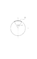
従来のEUV縮小投影露光装置1000の要部概略を図12に示す。図12において、1001はEUV光の発光点、1002はEUV光束、1003はフィルタ、1004は第1の回転放物面ミラー、1005は反射型インテグレータ、1006は第2の回転放物面ミラー、1007は反射型マスク、1008は投影光学系を構成する複数のミラー系、1009はウエハ、1010はマスクステージ、1011はウエハステージ、1012は円弧状アパーチャ、1013はレーザ光源、1014はレーザ集光光学系、1017は真空容器である。また図14は、マスク1007上の照明領域1015と露光が行なわれる円弧状領域1016との関係を示す平面図である。
FIG. 12 shows an outline of a main part of a conventional EUV reduction
このように露光装置1000は、EUV光を生成する光源部1013および1014、照明光学系(即ち、第1の回転放物面ミラー1004、反射型インテグレータ1005及び第2の回転放物面ミラー1006)、反射型マスク1007、投影光学系1008、ウエハ1009、マスクを搭載したステージ1010、ウエハを搭載したステージ1011、マスクやウエハの位置を精密に合わせる不図示のアライメント機構、EUV光の減衰を防ぐために光学系全体を真空に保つための真空容器1017と不図示の排気装置からなる。
As described above, the
照明光学系は、発光点1001からのEUV光1002を第1の回転放物面ミラー1004で集光し、反射型インテグレータ1005に照射して2次光源を形成し、さらに、この2次光源からのEUV光を第2の回転放物面ミラー1006で重畳されるように集光し、マスク1007を均一に照明する。
The illumination optical system condenses the EUV light 1002 from the
反射型マスク1007は多層膜反射鏡の上にEUV吸収体などからなる非反射部を設けた転写パターンが形成されたものである。反射型マスク1007で反射された回路パターンの情報を有するEUV光は、投影光学系1008によってウエハ1009面上に結像する。
The
投影光学系1008は光軸中心に対して軸外の細い円弧状の領域が良好な結像性能をもつように設計されている。従って、露光はこの細い円弧状領域のみが利用されるように、ウエハ1009直前に円弧状の開口をもったアパーチャ1012が設けられている。そして矩型形状をしたマスク全面のパターンを転写するため、反射型マスク1007とウエハ1009が同時にスキャンして露光が行なわれる。
The projection
ここで投影光学系1008は複数の多層膜反射鏡によって構成され、マスク1007上のパターンをウエハ1009表面に縮小投影する構成となっており、通常、像側テレセントリック系が用いられている。なお、物体側(反射型マスク側)は、反射型マスク1007に入射する照明光束との物理的干渉を避けるために、通常、非テレセントリックな構成となっている。
Here, the projection
レーザ光源1013からのレーザ光はレーザ集光光学系1014により発光点1001の位置にある不図示のターゲットに集光され、高温のプラズマ光源1001を生成する。このプラズマ光源から熱輻射により放射されたEUV光1002は第1の回転放物面ミラー1004で反射して平行なEUV光束となる。この光束が反射型インテグレータ1005で反射して、多数の2次光源を形成する。
The laser light from the
この2次光源からのEUV光は第2の回転放物面ミラー1006で反射して反射型マスク1007を照明する。ここで該2次光源から第2の回転放物面ミラー1006、第2の回転放物面ミラー1006から反射型マスク1007までの距離は、第2の回転放物面ミラー1006の焦点距離に等しく設定されている。
The EUV light from the secondary light source is reflected by the
2次光源の位置に第2の回転放物面ミラー1006の焦点が位置しているので2次光源の1つから出たEUV光は反射型マスク1007を平行光束で照射する。投影光学系1008は2次光源の像が投影光学系1008の入射瞳面に投影される様に設計されており、これによりケーラー照明の条件が満たされている。即ち反射型マスク1007上のある1点を照明するEUV光は全ての2次光源から出たEUV光の重なったものである。
Since the focal point of the
マスク面上の照明領域1015は、図13に示すように、反射型インテグレータ1005の構成要素である凸又は凹面ミラーの反射面の平面形状と相似であり、実際に露光が行なわれる円弧領域1016を含むほぼ矩形領域である。投影光学系1008は2次光源の像が投影光学系1008の瞳面に投影されるように設計されている。
しかしながら、従来のEUV縮小投影露光装置には次の様な欠点があった。即ち、ウエハ1009の近傍に照明領域を規定するアパーチャ1012を設けているが、露光時に駆動するウエハからはアパーチャをある程度離さなければならず、露光領域がボケてしまう。
However, the conventional EUV reduction projection exposure apparatus has the following drawbacks. That is, the
また、反射型マスク1007の近傍に同様のアパーチャを設けることも考えられるが、同様の問題が生じる。更に、反射型マスク1007の近傍に同様のアパーチャを設ける場合には、反射型マスクに入射する光と反射型マスクから反射する光の両方を考慮しなければならないため、更に問題が深刻である。
Although it is conceivable to provide a similar aperture in the vicinity of the
更に、照明領域を規定するアパーチャとレチクルとの間に結像系を設けることも考えられるが、従来はその詳細な構成が明らかとされていなかった。 Further, although it is conceivable to provide an imaging system between the aperture defining the illumination area and the reticle, the detailed configuration has not been clarified so far.
そこで、上記従来技術の問題点に鑑み、本発明の例示的な目的は、照明領域を規定するアパーチャとレチクルとの間の結像系の好適な構成を明らかにするとともに、その結像系を有する照明光学系を用いた露光装置を提供することにある。 Therefore, in view of the above-described problems of the prior art, an exemplary object of the present invention is to clarify a preferable configuration of an imaging system between an aperture that defines an illumination area and a reticle, and to define the imaging system. An object of the present invention is to provide an exposure apparatus using the illumination optical system.
上記目的を達成するために、本発明の一側面としての露光装置は、光源からの光で反射型マスクを照明する照明光学系と、該反射型マスクのパターンを基板に投影する投影光学系とを有する露光装置において、前記照明光学系は、前記反射型マスクの照明領域を規定する視野絞りと、該視野絞りの開口からのを光を前記反射型マスクに導く結像系とを有し、前記結像系は、共軸光学系であり、前記結像系の前記反射型マスク側の主光線は、該共軸に対して傾斜角を持ち、該傾斜角は、前記投影光学系の前記反射型マスク側の主光線と前記反射型マスクの表面の法線とがなす角に略等しいことを特徴とする。 In order to achieve the above object, an exposure apparatus according to one aspect of the present invention includes an illumination optical system that illuminates a reflective mask with light from a light source, and a projection optical system that projects a pattern of the reflective mask onto a substrate. The illumination optical system includes a field stop that defines an illumination area of the reflective mask, and an imaging system that guides light from an opening of the field stop to the reflective mask. The imaging system is a coaxial optical system, and the principal ray on the reflective mask side of the imaging system has an inclination angle with respect to the coaxial axis, and the inclination angle is the same as that of the projection optical system. It is substantially equal to an angle formed by a principal ray on the reflective mask side and a normal line on the surface of the reflective mask.
本発明の更なる目的又はその他の特徴は、以下、添付の図面を参照して説明される好ましい実施例等によって明らかにされるであろう。 Further objects and other features of the present invention will be made clear by the preferred embodiments described below with reference to the accompanying drawings.
従来よりも、性能の良い露光装置を提供することができる。 It is possible to provide an exposure apparatus with better performance than before.
以下に、本発明の実施の形態を添付の図面に基づいて詳細に説明する。 Embodiments of the present invention will be described below in detail with reference to the accompanying drawings.
図1は本発明の第1の実施例の要部概略図である。同図において、1は励起レーザ光、2はEUV光を放射するプラズマ発光点、3aはプラズマ生成のターゲットとなる液滴を噴射するノズル、3bは励起レーザ光が照射されなかった液滴を回収して再利用するための液滴回収部、4はプラズマ発光点から放射される光束を受光する集光ミラー、6aはプラズマからの飛散粒子(デブリ)を除去するフィルタ、6bはEUV光以外の波長の光束を除去する波長フィルタ、7は集光ミラー4の集光点近傍に配置されたピンホール状のアパーチャ、8はプラズマ光源を収容する真空容器、であり、これらが光源部を構成している。なお、5はミラー4により集光されたEUV光束であり、9は露光装置本体とプラズマ光源部を真空状態で接続するための接続部である。
FIG. 1 is a schematic view of the main part of a first embodiment of the present invention. In the figure, 1 is an excitation laser beam, 2 is a plasma emission point that emits EUV light, 3a is a nozzle that ejects a droplet that is a target for plasma generation, and 3b is a droplet that is not irradiated with an excitation laser beam. A liquid droplet collecting unit 4 for reusing the light, 4 is a condensing mirror for receiving a light beam emitted from a plasma emission point, 6a is a filter for removing scattered particles (debris) from the plasma, and 6b is other than EUV light. A wavelength filter that removes a light beam having a wavelength, 7 is a pinhole-shaped aperture disposed near the condensing point of the
次に、10a、10bはアパーチャ7を通過したEUV光束を受光し、ほぼ平行光束に変換するための凹面ミラーと凸面ミラーからなる平行変換光学系である。11aは複数の円筒面ミラーを有するインテグレータ、11b、11cはインテグレータ11aからの光束を円弧状に集光するための回転放物面ミラーを含んだ光学系である。11a、11b、11cで円弧変換光学系を形成している。12、13はスリット系(視野絞り)を構成しており、12は円弧状の開口部を有し、その幅を部分的に可変できるスリット、13は反射型マスク16と共役な面に配置され、所望の露光領域に照明光を制限するためのマスキングブレードである。14はマスキング結像系であって、マスキングブレード13を物体側、反射マスク16面を像側として所望の倍率で結像し、円弧照明領域を反射マスク上に形成する。14a、14b、14c、14dは光学系でありマスキング結像系14を構成する曲面ミラー、14eは結像系14a〜14dからの光束を反射してマスキング結像系14の像側光束14'を反射マスク16へはね上げて所定の角度で入射させるための平面ミラー、15は結像系14a〜14dの瞳面に配置された開口絞りであり、以上が、光源部からの光で反射マスク16を照明する照明光学系を構成する。
Next, 10a and 10b are parallel conversion optical systems comprising a concave mirror and a convex mirror for receiving the EUV light beam that has passed through the aperture 7 and converting it into a substantially parallel light beam. 11a is an integrator having a plurality of cylindrical surface mirrors, and 11b and 11c are optical systems including a rotating paraboloid mirror for condensing the luminous flux from the
そして、17は反射マスク16を保持するマスクステージ、18は複数枚のミラーにより構成される投影光学系であり共軸光学系となっており物体側が非テレセンで像側がテレセンになるように設計されている。19は感光材が塗布されたウエハ、20はウエハ19を保持するウエハステージ、21はEUV光の減衰を防ぐために光学系全体を真空に保つための真空容器である。
不図示の励起レーザ光源及び集光光学系から成る励起レーザ部から放射された、高出力の励起パルスレーザ光1は、発光点2の位置に集光するように構成されており、レーザプラズマ光源部を形成している。このレーザプラズマ光源のターゲットとなる液滴(例えばXeから成る)は、ノズル3aから一定の時間間隔で連続的に噴射され、集光点2を通過するようになっている。そして上記のように噴射された液滴が、ちょうど2の位置にきた時に、励起パルスレーザ光1がその液滴を照射することで高温のプラズマ発光点2を生成し、このプラズマからの熱輻射によってEUV光が発生する。
A high-power excitation
なお、本実施例ではターゲットとしてXeの液滴を用いた形態を示しているが、ターゲットとしてはXeガスをノズルから真空中に噴射して、断熱膨張により生じるクラスタを用いたり、Xeガスを金属表面で冷却して固体化したものを用いたり、Cu等の金属テープを用いたものを選択してもよい。あるいは、EUV光源としてアンジュレータを用いてもよい。また、EUV光源としてZピンチ方式、プラズマ・フォーカス、キャピラリー・ディスチャージ等の所謂ディスチャージ方式によるプラズマ光源を用いてもよい。 In this embodiment, Xe droplets are used as the target. However, as the target, Xe gas is injected into the vacuum from the nozzle to use a cluster generated by adiabatic expansion, or Xe gas is made of metal. You may use what was solidified by cooling on the surface, or what used metal tapes, such as Cu. Alternatively, an undulator may be used as the EUV light source. Further, a so-called discharge system plasma light source such as a Z-pinch system, plasma focus, capillary discharge, etc. may be used as the EUV light source.
プラズマ発光点2から放射されたEUV光は、回転楕円ミラー等による集光ミラー4により集光されてEUV光束として取りだされ、フィルタ6aによりプラズマ及びその周辺から直接前方へ飛ぶ飛散粒子(デブリ)を除去され、さらに必要に応じてフィルタ6bによりEUV露光に不要な波長成分を除去されて、プラズマ光源を収容する真空容器8と、露光装置本体の真空容器21の境界面に設けられたピンホール状のアパーチャ7の位置に集光される。光源の真空容器8と露光装置本体の真空容器21は、接続部9で接続されている。
The EUV light radiated from the
上記アパーチャ7を通過したEUV光束5は、中心部分に開口部を有する凹面ミラー10aとそのミラーと比べて比較的小径の凸面ミラー10bからなる平行変換光学系によりほぼ平行な光束10'に変換される。ここで、凹面ミラー10aは凸面ミラー10bによって反射された光が通過するための開口を有し、その開口は光源からのEUV光束の光軸近傍に配置されている。また、これらのミラー10a,10bは、光源からのEUV光束の光軸に対して、略回転対称となるような反射面を有しており、中心軸とそのEUV光束の光軸とがほぼ一致している。
The EUV light beam 5 that has passed through the aperture 7 is converted into a substantially
ここで上記の集光ミラー4及びミラー10a、10bは、EUV光を効率良く反射するための反射多層膜が成膜されており、高温のプラズマ2からの放射エネルギーを一部吸収するために、露光中に高温になる。そのために材質としては熱伝導性の高い金属等の材料を用いるとともに、水冷など不図示の冷却手段を有しており、露光中は常に冷却されている。
Here, the above-mentioned condenser mirror 4 and mirrors 10a and 10b are formed with a reflective multilayer film for efficiently reflecting EUV light, and in order to partially absorb the radiation energy from the high-
また、以下では特に明示しないが、光学系に用いられている各ミラーの反射面には、EUV光を効率良く反射するための反射多層膜が成膜されており、必要に応じてミラーは熱伝導性の高い金属等の材料を用いたり、冷却手段を装備したりしている。 Although not specified below, a reflective multilayer film for efficiently reflecting EUV light is formed on the reflective surface of each mirror used in the optical system, and the mirror is heated as necessary. They use materials such as highly conductive metals and are equipped with cooling means.
次に、ほぼ平行な光束に変換されたEUV光10'は、複数の反射型円筒面ミラーを有するインテグレータ11aに入射し、各円筒面により分割されて発散する光束が、平面ミラー11bと回転放物面ミラー11cにより円弧状に集光される事で、円弧スリット12の開口部に均一な照度分布をもつ円弧照明領域を形成する。
Next, the EUV light 10 ′ converted into a substantially parallel light beam is incident on an
ここで、インテグレータ11aによって円弧領域を均一に照明する原理について、別の図を用いて詳細に説明する。
Here, the principle of uniformly illuminating the arc region by the
図3(a)は複数の凸円筒面をもった反射型凸円筒面インテグレータ11aに平行光が入射した場合の摸式的斜視図であって、前記のほぼ平行なEUV光束10'は図示した方向から入射する。また図3(b)は、図3(a)と同様の効果を有する複数の凹円筒面をもった反射型凹円筒面インテグレータの模式的斜視図である。図1のインテグレータ11aは、図3(a)で示されるような反射型凸円筒面インテグレータであるが、図3(b)で示されるような反射型凹円筒面インテグレータでも、あるいはこれらの凹凸の組み合わせであっても良い。
FIG. 3A is a schematic perspective view in the case where parallel light is incident on a reflective convex
図4は反射型凸円筒面インテグレータの摸式的断面図、図5は反射型凸円筒面インテグレータの円筒面でのEUV光反射の説明図、図6は反射型凸円筒面インテグレータの円筒面で反射したEUV光束の角度分布図である。各図中、符号11aは反射型凸円筒面インテグレータを示している。
4 is a schematic sectional view of the reflective convex cylindrical surface integrator, FIG. 5 is an explanatory diagram of EUV light reflection on the cylindrical surface of the reflective convex cylindrical surface integrator, and FIG. 6 is a cylindrical surface of the reflective convex cylindrical surface integrator. It is an angle distribution map of the reflected EUV light beam. In each figure,
図3(a)の様に、複数の円筒面をもったインテグレータ11aにほぼ平行なEUV光束11を入射すると、このインテグレータの表面近傍に線状の2次光源が形成されると共に、この2次光源から放射されるEUV光束の角度分布が円錐面状となる。次にこの2次光源位置を焦点とする反射鏡で前記EUV光束を反射して反射マスクあるいは反射マスクと共役な面を照明することにより、円弧形状の照明が可能となる。
As shown in FIG. 3A, when a substantially parallel EUV light beam 11 is incident on an
複数の円筒面をもった反射型インテグレータの作用を説明するために、まず、一つの円筒面反射鏡に平行光が入射した場合の反射光の振る舞いについて図5を用いて述べる。今、一つの円筒面にその中心軸に垂直な面に対してθの角度で平行光を入射する場合を考える。平行な入射光の光線ベクトルを
P1=(0,−cosθ,sinθ)
円筒面形状の反射面の法線ベクトルを
n=(−sinα,cosα,0)
とすると、反射光の光線ベクトルは
P2=(−cosθ×sin2α,cosθ×cos2α,sinθ)
となる。このとき反射光の光線ベクトルを位相空間にプロットすれば、図6に示すようにxy平面上で半径cosθの円となる。即ち、反射光は円錐面状の発散光となり、この円錐面の頂点の近傍に2次光源が存在することになる。この2次光源はインテグレータ11aの円筒面が凹面であれば反射面の外部に実像として存在し、凸面であれば反射面の内部に、虚像として存在することになる。また図4に示すように反射面が円筒面の一部に限られていて、その中心角が2φである場合は、図6に示すように反射光の光線ベクトルP2の存在範囲はxy平面上で中心角4φの円弧601となる。
In order to explain the operation of the reflective integrator having a plurality of cylindrical surfaces, first, the behavior of the reflected light when parallel light enters one cylindrical surface reflecting mirror will be described with reference to FIG. Consider a case where parallel light is incident on one cylindrical surface at an angle θ with respect to a plane perpendicular to the central axis. The ray vector of parallel incident light is P1 = (0, −cos θ, sin θ)
The normal vector of the cylindrical reflecting surface is n = (− sin α, cos α, 0)
Then, the ray vector of the reflected light is P2 = (− cos θ × sin 2α, cos θ × cos 2α, sin θ).
It becomes. If the ray vector of the reflected light is plotted in the phase space at this time, it becomes a circle of radius cos θ on the xy plane as shown in FIG. That is, the reflected light becomes a conical divergent light, and a secondary light source exists near the apex of the conical surface. If the cylindrical surface of the
次に、上述した円筒面反射鏡に平行光が入射して形成される2次光源の位置近傍に焦点をもつ、焦点距離fの回転放物面ミラーと、さらにこの反射鏡からfだけ離れた位置に被照射面を配置した場合を考える。2次光源から出た光は円錐面状の発散光になり焦点距離fの反射鏡で反射したのち、平行光となる。このときの反射光は半径f×cosθで中心角4φの円弧状断面のシートビームになる。従って図6で示した様に、被照射面上の半径f×cosθで中心角4φの円弧状領域601のみが照明されることになる。
Next, a rotary paraboloidal mirror having a focal length f having a focal point near the position of the secondary light source formed by the parallel light incident on the cylindrical surface reflecting mirror described above, and further away from the reflecting mirror by f. Consider a case where the irradiated surface is arranged at a position. The light emitted from the secondary light source becomes a conical divergent light that is reflected by a reflecting mirror having a focal length f and then becomes parallel light. The reflected light at this time is a sheet beam having an arcuate cross section with a radius of f × cos θ and a central angle of 4φ. Therefore, as shown in FIG. 6, only the arc-shaped
これまでは1つの円筒面反射鏡について説明してきたが、次に、多数の円筒面を平行に多数並べた広い面積のインテグレータ11aに、ある光束径を有する平行光10'が図1に示した方向に入射した場合について、図2を用いて説明する。
Up to now, one cylindrical surface reflecting mirror has been described. Next, parallel light 10 ′ having a certain light beam diameter is shown in FIG. 1 in a
図2において、11aは前述したインテグレータ、11bは平面ミラー、11cは回転放物面ミラー、12は円弧状の開口部を有するスリットである。回転放物面ミラー11cは、軸201AXを中心対称軸とし、点202を焦点とする放物線を、軸201AXを回転軸として回転させて形成される面の一部を反射面とするミラーであって、焦点202とミラー面有効部中心点204との距離が、焦点距離fとなる。また、点204と円弧スリット12の距離は、ほぼ前述の焦点距離fに等しくなるように配置されている。
In FIG. 2, 11a is the integrator described above, 11b is a plane mirror, 11c is a paraboloidal mirror, and 12 is a slit having an arcuate opening. The paraboloidal mirror 11c is a mirror having a reflecting surface as a part of a surface formed by rotating a parabola with the axis 201AX as a central axis of symmetry, a parabola with the
そして回転放物面ミラー11cは、その回転軸201AXがインテグレータ11aの反射面近傍(反射面含む)に、反射面と平行かつ表面の円筒面の並びに沿うように配置されている。そして回転放物面ミラー11cの有効部中心点204と焦点202の間には、平面ミラー11bが図に示すように配置されており、焦点202のミラー11b反射面に対して対称な点202'が、インテグレータ11aの反射面有効部のほぼ中心位置にくるような構成となっている。即ち、位置204から位置202'への光路長が焦点距離fに等しい。
The rotating paraboloidal mirror 11c is arranged so that the rotation axis 201AX is in the vicinity of the reflecting surface (including the reflecting surface) of the
このような配置にした場合、位置202'と円弧スリット12は、回転放物面ミラー11bに対して互いに焦点距離fだけ離れた関係、即ち互いにほぼフーリエ変換面の関係となり、ほぼ平行なEUV光束10'が図のようにインテグレータ11aに入射した場合は、円弧スリット12の開口部近傍に集光される。
In such an arrangement, the
この時、回転放物面ミラー11cへのEUV光束主光線の入射角ξは低入射角度(0°より大きく45°以下の角度)、具体的には20°以下に設定されており、これにより入射角ξが高入射角となるような配置にするよりも、円弧スリット12への集光の際に生じるボケ量を小さくして、円弧開口部近傍への集光効率を高めることができる。これによりケラレによる光の損失を抑える事が可能となり、照明系効率の向上をもたらすことができる。 At this time, the incident angle ξ of the principal ray of the EUV light beam on the rotating parabolic mirror 11c is set to a low incident angle (an angle greater than 0 ° and equal to or less than 45 °), specifically 20 ° or less. Rather than an arrangement in which the incident angle ξ is a high incident angle, the amount of blur that occurs when condensing light to the arc slit 12 can be reduced, and the light condensing efficiency near the arc opening can be increased. As a result, light loss due to vignetting can be suppressed, and illumination system efficiency can be improved.
次に円筒面を平行に多数並ベた反射鏡で反射された光の角度分布は、先の例と変わらないので、インテグレータ11aへの光束入射角をεとすると、円弧スリット12の近傍には半径f×cosεの円弧状領域が照明されることになる。また、円弧スリット12近傍の一点に入射する光は、円筒面を平行に多数並べた反射鏡の照射領域全域から到達するので、ほぼ平行なEUV光束10'の光束径をDとすると、その角度広がり(すなわち集光NA)γはγ=D/fとなる。
Next, the angular distribution of the light reflected by the reflecting mirrors having a large number of cylindrical surfaces arranged in parallel is not different from the previous example. Therefore, assuming that the incident angle of the light beam to the
この時、円弧照明領域において、その円弧に沿った方向に対して、インテグレータ11aの多数の円筒面からの各光束が重畳されることで、照度の均一性が達成されている。即ちこれにより効率がよく均一な円弧照明を行なうことが可能となる。
At this time, in the arc illumination area, uniformity of illuminance is achieved by superimposing the light beams from the many cylindrical surfaces of the
ここで図1に戻り、本実施例の露光方法について引き続き説明する。同図において円弧スリット12の開口部近傍に形成された円弧照明領域は、マスキングブレード13によりその領域の一部を制限され、マスキング結像系14により所望の倍率で拡大または縮小されて、マスクステージ17に保持された反射型マスク16上に、所望の入射角度で入射して円弧照明領域を形成することで反射マスク16に対して円弧照明を行なう。なおこの円弧状の照明領域の曲率中心は、投影光学系18の光軸18AXにほぼ一致している。
Here, returning to FIG. 1, the exposure method of this embodiment will be described. In the figure, the arc illumination area formed in the vicinity of the opening of the arc slit 12 is partially limited by the
この円弧照明された反射型マスク16からの回路パターン情報を有するEUV反射光は、投影光学系18により露光に最適な倍率で、感光材が塗布されたウエハ19に投影結像されることで、回路パターンの露光が行なわれる。
The EUV reflected light having circuit pattern information from the
上記ウエハ19はウエハステージ20に固定されており、紙面上で上下前後に平行移動する機能を持ち、その移動は不図示のレーザ干渉計等の測長器で制御されている。そして、投影光学系18の倍率をMとすると、例えば反射型マスク16を紙面に平行な方向に速度vで走査すると同時に、ウエハ19を紙面に平行な方向に速度v/Mにて同期走査することで、全面スキャン露光が行なわれる。
The
上記投影光学系18は複数の多層膜反射鏡によって構成され、光軸中心18AXに対して軸外の細い円弧状の領域が良好な結像性能をもつように設計されている。そして反射型マスク16上のパターンをウエハ19表面に縮小投影する構成となっており、像側(ウエハ側)テレセントリック系となっている。そして物体側(反射型マスク側)は、反射型マスク16に入射する照明光束との物理的干渉を避けるために、通常、非テレセントリックな構成となっており、例えば本実施例においては、物体側主光線はマスク16の法線方向に対して約6°傾いている。
The projection
以下では、
・円弧照明によるスキャン露光について
・円弧スリット12による露光ムラ補正方法
・スキャン露光時のマスキングブレード13の動作
・マスキング結像系の構成
について順を追って詳細に説明する。
Below,
Scan exposure with arc illumination. Exposure unevenness correction method with arc slit 12. Operation of masking
図7(a)及び図7(b)は、それぞれウエハ面におけるスキャン露光開始および終了の状態を示す図である。同図において、701はウエハ面上の円弧照明領域であり、702は露光対象となる露光領域である。この図では露光領域702はウエハステージ駆動により紙面の左から右へ移動し、円弧照明領域701が相対的に露光領域702を走査するようになっている。露光開始及び終了の段階で、円弧照明領域701が露光領域702以外の部分を照明しているが、これを防ぐためにマスキングブレードが遮光するようになっている。これについては後のマスキングブレードの動作の説明のところで述べる。
FIGS. 7A and 7B are diagrams showing the states of the start and end of scan exposure on the wafer surface, respectively. In the figure,
なおこの例で示した走査方向に対して、相対的に逆方向に走査して露光を行なう場合についても同様である。 The same applies to the case where exposure is performed by scanning in a direction opposite to the scanning direction shown in this example.
上記のスキャン露光において、円弧スリット12により露光ムラを補正する方法の詳細について図8を用いて説明する。同図において、810は円弧スリット12のスリット幅811を部分的に変えるための可動エッジ部が多数並んだものであり、811は円弧照明領域を形成するためのスリット開口部、812は前述したインテグレータ11a及びミラー系11b、11cにより形成された円弧照射領域であって、この照射領域からスリット開口部811を通過する光束を切り出すようになっている。
Details of a method of correcting exposure unevenness by the arc slit 12 in the above-described scan exposure will be described with reference to FIG. In the figure,
ここでスキャン露光時において、反射型マスク16の回路パターンをウエハ19に縮小して転写する際に、円弧スリット内に照度ムラがあるとスキャン露光した際に露光ムラが発生する。この問題を解消するために、円弧スリット内で照度が相対的に強い部分のスリット幅のみを、可動エッジ部810を不図示の駆動系で動かすことにより少し狭くして、所望の量だけ光量を少し減らしてスキャン露光することで、露光領域全面で積算した結果として均一な強度で露光することが可能となる。
Here, at the time of scan exposure, when the circuit pattern of the
またマスキングブレード13は、801、802、803、804の4枚の遮光板により構成されており、図8において上下の遮光板803、804は、円弧スリット開口811における円弧照射領域812の両端を遮光する事で、図7(a)に示した露光領域702の上下幅(スキャン幅)を決定している。
Further, the
遮光板801及び802はスキャン露光においてワンショットの露光開始から終了までの間に、それぞれ左右方向に移動して隙間を開閉する事で、露光領域702の左右幅(スキャン長さ)を決定している。これについて図9を用いて以下に説明する。
The
図9において(a1)から(a5)は、スキャン露光の開始から終了までを時系列に表現したものであり、(b1)から(b5)はそれぞれ(a1)から(a5)の状態におけるマスキングブレード13の遮光板801及び802の動きを示したものである。
In FIG. 9, (a1) to (a5) represent the time series from the start to the end of scan exposure, and (b1) to (b5) are masking blades in the states (a1) to (a5), respectively. 13 shows the movement of thirteen
露光が開始されようとしている(a1)の状態になった時、(b1)にて遮光板802は右に移動を開始して、隙間を開く動作に入る。この時、円弧照明領域701は遮光されている状態なので、図示はしてあるが実際には照明はされていない状態である。そして(a2)に示すようにスキャン露光に入った段階で、円弧照明領域701が露光領域702からはみ出している部分がちょうど遮光されるように、(b2)に示すような状態で遮光板802が移動していく。さらに(a3)のように露光領域702内に円弧照明領域701が入っておりスキャン露光されている時には、(b3)のように遮光板802はスリット開口部811が完全に開いた状態になるように右に移動している。次に(a4)のようにスキャン露光が終了近くなってくると、今度は遮光板801が右に移動して、円弧照明領域701が露光領域702からはみ出している部分がちょうど遮光される。そして(a5)のようにスキャン露光が完了したときには、遮光板801がスリット開口部811を完全に覆うように移動している。以上の一連の動作によって、所望の露光領域に対してスキャン露光が行なわれる。
When the exposure is about to start (a1), the
次に、マスキング結像系14の詳細について図10を用いて説明する。マスキング結像系14は、前述したマスキングブレード13を物体面、反射型マスク16(図では位置102)を像面とし、反射多層膜を成膜したミラーにより構成される結像光学系である。この結像系は共軸光学系であり、共軸(光軸)10AXを略中心とする物体側の円弧領域に対して所望の倍率をかけて、投影系18に対して好適な円弧照明領域を形成するように結像する機能を有する。
Next, details of the masking
同図において、14a、14b、14c、14dはそれぞれ中心軸10AXを回転対称軸とする、凹面又は凸面の球面または非球面から成るミラーであって、本実施例においては、14aから順番に凹凹凸凹の形状となっている。またマスキング結像系14の瞳面はミラー14bの反射面近傍(反射面含む)にあり、瞳面の近傍(瞳面含む)に開口絞り15を配置している。この開口絞り15の開口パターンを変える事で、開口の大きさ又は形状を変更することができ、つまり、反射マスク側の照明光束の収束角(いわゆるコヒーレントファクタσ)を変えたり、変形照明を行なったりすることが可能であるが、詳細は後述する。
In the figure,
円弧スリット12の近傍に配置したマスキングブレード13の位置に集光したEUV光束は、その主光線が回転対称軸10AXに対して平行な状態すなわち物体側テレセンで、マスキング結像系14に入射する。入射した光束は上述した4枚のミラー及び開口絞り15を経て、像面102へ集光される。この時注意すべきは、像側は非テレセンな構成となっていることであり、主光線103の像面102への入射角度101(主光線103と回転対称軸10AXのなす角度)は、投影系18の物体側主光線のマスク面法線に対する傾斜角とほぼ等しくなるように設定されていることである。つまり、反射型マスクの照明領域内の各位置に対応する、結像系14a〜dのマスク側主光線と回転対称軸10AXとのなす角度は、投影光学系のマスク側主光線とマスク面の法線とのなす角度とほぼ等しくなるように設定されている。本実施例の場合、入射角度101は約6°に設定されており、投影光学系18のマスク側の対応する主光線とマスク面の法線とのなす角度と等しくなっている。なお、投影光学系の光軸(共軸)18AXとマスク面の法線とが平行であることから、投影光学系の光軸18AXと投影光学系のマスク側の対応する主光線とがなす角度もそれと等しくなっている。従って、結像系のマスク側主光線の結像系の光軸に対する角度は、投影光学系のマスク側主光線とマスク面法線とのなす角と略等しくなっている。なお結像系は、像側のボケについても良好に補正されており、像面でスポット径が5mm以下、望ましくは1mm以下になるように設計されている。
The EUV light beam condensed at the position of the
図1で示したマスキング結像系14の像側光束14'においては、平面ミラー14eで像側光束を反射マスク16の方向へはね上げた時に、平面ミラー14eによる反射によって光束14'が形成する円弧照明領域の円弧の向きは反転して、且つその円弧の中心は投影系18の中心軸18AXと反射マスク面の交点にほぼ一致している。そして上記で示したように入射角度101を設定することで、上記の光束14'の主光線と投影系18の物体側光束18'の対応する主光線が、反射マスクを反射面として互いにほぼ一致するように配置する事が可能となる。
In the image-
次にマスキング結像系14における開口絞り15の切り替えにより、コヒーレントファクタσを変えたり、輪帯照明等の変形照明を行なったりする方法について述べる。開口絞り15(即ちマスキング結像系の瞳面)と投影系18の瞳面は、互いに共役な関係にあるので、開口絞り15の開口パターンつまり光束の透過パターンが、投影系瞳面における光源像即ち有効光源分布と対応している。図11は、開口絞り15が有する開口部の形状の例を示す図であり、(a)は通常照明の大σ、(b)は通常照明の小σ、(c)は輪帯照明、(d)は四重極照明の各モードに対応している。
Next, a method of changing the coherent factor σ or performing modified illumination such as annular illumination by switching the
このようないくつかの開口パターンを例えばターレットとして用意しておき、不図示の開口絞り駆動系によりこのターレットを回転させることで、所望の開口形状に切り替えることが可能である。また、ターレットを用いずに他の機械的な方法、例えば複数の開口絞りを並べておいて、順次切り替えてももちろん構わないし、虹彩絞りを使用してももちろん良い。 It is possible to switch to a desired aperture shape by preparing several such aperture patterns as a turret, for example, and rotating the turret by an aperture stop driving system (not shown). Also, other mechanical methods without using the turret, for example, a plurality of aperture stops may be arranged side by side and switched sequentially, or an iris stop may be used.
次に、実施例1の露光装置を利用したデバイスの製造方法の実施例を説明する。図15はデバイス(ICやLSI等の半導体チップ、液晶パネルやCCD)の製造フローを示す。ステップ1(回路設計)では半導体デバイスの回路設計を行なう。ステップ2(マスク製作)では設計した回路パターンを形成したマスク(レチクル)を製作する。一方、ステップ3(ウエハ製造)ではシリコン等の材料を用いて基板(被処理体)としてのウエハを製造する。ステップ4(ウエハプロセス)は前工程と呼ばれ、上記用意したマスクとウエハとを用いて、リソグラフィ技術によってウエハ上に実際の回路を形成する。次のステップ5(組み立て)は後工程と呼ばれ、ステップ4よって作成されたウエハを用いてチップ化する工程であり、アッセンブリ工程(ダイシング、ボンディング)、パッケージング工程(チップ封入)等の工程を含む。ステップ6(検査)ではステップ5で作成された半導体デバイスの動作確認テスト、耐久性テスト等の検査を行なう。こうした工程を経て半導体デバイスが完成し、これが出荷(ステップ7)される。
Next, an embodiment of a device manufacturing method using the exposure apparatus of
図16は上記ウエハプロセスの詳細なフローを示す。ステップ11(酸化)ではウエハの表面を酸化させる。ステップ12ではウエハの表面に絶縁膜を形成する。ステップ13(電極形成)ではウエハ上に電極を蒸着によって形成する。ステップ14(イオン打ち込み)ではウエハにイオンを打ち込む。ステップ15(レジスト処理)ではウエハにレジスト(感材)を塗布する。ステップ16(露光)では実施例1の露光装置によってマスクの回路パタ−ンの像でウエハを露光する。ステップ17(現像)では露光したウエハを現像する。ステップ18(エッチング)では現像したレジスト以外の部分を削り取る。ステップ19(レジスト剥離)ではエッチングが済んで不要となったレジストを取り除く。これらステップを繰り返し行なうことによりウエハ上に回路パタ−ンが形成される。
FIG. 16 shows a detailed flow of the wafer process. In step 11 (oxidation), the wafer surface is oxidized. In
本実施例の製造方法を用いれば、従来は難しかった高集積度のデバイスを製造することが可能になる。 By using the manufacturing method of this embodiment, it becomes possible to manufacture a highly integrated device, which has been difficult in the past.
以上、本発明の好ましい実施例について説明したが、本発明はこれらの実施例に限定されないことはいうまでもなく、その要旨の範囲内で種々の変形及び変更が可能である。例えば、本実施形態では13.5nmのEUV光を用いる照明系について説明したが、本発明はその他の光(例えば、波長200nm〜10nmの極端紫外線領域(EUV)又はX線領域の光)を用いる照明光学系にも適用することができる。なお、20〜5nmの光に対しては、レンズとして使用できる硝材は存在せず光学系をミラーで構成する必要があるため、その領域の光を用いる照明光学系に本発明を適用するとより有効である。 The preferred embodiments of the present invention have been described above, but the present invention is not limited to these embodiments, and various modifications and changes can be made within the scope of the gist. For example, although an illumination system using 13.5 nm EUV light has been described in the present embodiment, the present invention uses other light (for example, light in the extreme ultraviolet region (EUV) or X-ray region having a wavelength of 200 nm to 10 nm). The present invention can also be applied to an illumination optical system. For light of 20 to 5 nm, there is no glass material that can be used as a lens, and it is necessary to configure the optical system with a mirror. Therefore, it is more effective to apply the present invention to an illumination optical system that uses light in that region. It is.
1 励起レーザ光
2 プラズマ発光点
4 集光ミラー
8 真空容器
10a 平行変換光学系
10b 平行変換光学系
11a インテグレータ
12 可変円弧スリット
13 マスキングブレード
14 マスキング結像系
15 開口絞り
16 反射型マスク
17 マスクステージ
18 投影光学系
19 ウエハ
20 ウエハステージ
21 真空容器
DESCRIPTION OF
Claims (13)
前記照明光学系は、前記反射型マスクの照明領域を規定する視野絞りと、該視野絞りの開口からの光を前記反射型マスクに導く結像系とを有し、
前記結像系は、共軸光学系であり、
前記結像系の前記反射型マスク側の主光線は、該共軸に対して傾斜角を持ち、
該傾斜角は、前記投影光学系の前記反射型マスク側の主光線と前記反射型マスク表面の法線とがなす角と等しいことを特徴とする露光装置。 In an exposure apparatus having an illumination optical system that illuminates a reflective mask with light from a light source, and a projection optical system that projects a pattern of the reflective mask onto a substrate,
The illumination optical system includes a field stop that defines an illumination area of the reflective mask, and an imaging system that guides light from an opening of the field stop to the reflective mask,
The imaging system is a coaxial optical system;
The principal ray on the reflective mask side of the imaging system has an inclination angle with respect to the coaxial axis,
The exposure apparatus according to claim 1, wherein the inclination angle is equal to an angle formed by a principal ray on the reflective mask side of the projection optical system and a normal line of the reflective mask surface.
前記円弧の曲率中心は、前記共軸上又はその近傍にあることを特徴とする請求項1記載の露光装置。 The field stop has an arc slit having an arc-shaped opening,
Center of curvature of the arc, the exposure apparatus according to claim 1, characterized in that there the co-axial or near.
該円弧の曲率中心は、前記共軸近傍にあることを特徴とする請求項1記載の露光装置。 The illumination optical system includes a reflective integrator that forms a plurality of secondary light sources with light from the light source, and a mirror that forms an arcuate illumination region by superimposing the light beams from the plurality of secondary light sources on the field stop And having a system
2. The exposure apparatus according to claim 1, wherein the center of curvature of the arc is in the vicinity of the coaxial axis.
前記4枚のミラーのうち前記視野絞りから1枚目のミラーと4枚目のミラーの反射面は、凹面であることを特徴とする請求項1記載の露光装置。 The imaging system has four mirrors,
The reflecting surface of the first sheet of mirrors and 4th mirrors from the field stop of the four mirrors, the exposure apparatus according to claim 1, wherein the concave.
Priority Applications (6)
| Application Number | Priority Date | Filing Date | Title |
|---|---|---|---|
| JP2003324639A JP4241281B2 (en) | 2003-09-17 | 2003-09-17 | Exposure equipment |
| EP04001822A EP1517339A3 (en) | 2003-09-17 | 2004-01-28 | Illumination optical system and exposure apparatus |
| TW093102016A TWI267127B (en) | 2003-09-17 | 2004-01-29 | Illumination optical system and exposure apparatus |
| US10/769,373 US7110084B2 (en) | 2003-09-17 | 2004-01-30 | Illumination optical system and exposure apparatus |
| US10/768,896 US7064806B2 (en) | 2003-09-17 | 2004-01-30 | Illumination optical system and exposure apparatus |
| KR1020040074612A KR100687655B1 (en) | 2003-09-17 | 2004-09-17 | Illumination optical system and exposure apparatus |
Applications Claiming Priority (1)
| Application Number | Priority Date | Filing Date | Title |
|---|---|---|---|
| JP2003324639A JP4241281B2 (en) | 2003-09-17 | 2003-09-17 | Exposure equipment |
Publications (3)
| Publication Number | Publication Date |
|---|---|
| JP2005093693A JP2005093693A (en) | 2005-04-07 |
| JP2005093693A5 JP2005093693A5 (en) | 2006-10-19 |
| JP4241281B2 true JP4241281B2 (en) | 2009-03-18 |
Family
ID=34191311
Family Applications (1)
| Application Number | Title | Priority Date | Filing Date |
|---|---|---|---|
| JP2003324639A Expired - Fee Related JP4241281B2 (en) | 2003-09-17 | 2003-09-17 | Exposure equipment |
Country Status (5)
| Country | Link |
|---|---|
| US (2) | US7064806B2 (en) |
| EP (1) | EP1517339A3 (en) |
| JP (1) | JP4241281B2 (en) |
| KR (1) | KR100687655B1 (en) |
| TW (1) | TWI267127B (en) |
Families Citing this family (12)
| Publication number | Priority date | Publication date | Assignee | Title |
|---|---|---|---|---|
| JP4241295B2 (en) * | 2003-09-26 | 2009-03-18 | キヤノン株式会社 | Stage equipment |
| JP4458330B2 (en) * | 2003-12-26 | 2010-04-28 | キヤノン株式会社 | Replacing the multilayer mirror of the light source unit |
| JP2005317611A (en) * | 2004-04-27 | 2005-11-10 | Canon Inc | Exposure method and aligner |
| US8873151B2 (en) * | 2005-04-26 | 2014-10-28 | Carl Zeiss Smt Gmbh | Illumination system for a microlithgraphic exposure apparatus |
| CN101218543A (en) * | 2005-06-14 | 2008-07-09 | 皇家飞利浦电子股份有限公司 | Debris mitigation system with improved gas distribution |
| WO2007001624A2 (en) * | 2005-06-28 | 2007-01-04 | Microchips, Inc. | Medical and dental implant devices for controlled drug delivery |
| KR100729263B1 (en) * | 2005-07-14 | 2007-06-15 | 삼성전자주식회사 | Substrate exposure apparatus |
| JP4986754B2 (en) * | 2007-07-27 | 2012-07-25 | キヤノン株式会社 | Illumination optical system and exposure apparatus having the same |
| JP2009176838A (en) * | 2008-01-22 | 2009-08-06 | Canon Inc | Immersion lithography apparatus and method of manufacturing device |
| DE102008001553B4 (en) * | 2008-05-05 | 2015-04-30 | Carl Zeiss Smt Gmbh | Component for setting a scan-integrated illumination energy in an object plane of a microlithography projection exposure apparatus |
| US8227778B2 (en) * | 2008-05-20 | 2012-07-24 | Komatsu Ltd. | Semiconductor exposure device using extreme ultra violet radiation |
| JP5534910B2 (en) * | 2009-04-23 | 2014-07-02 | ギガフォトン株式会社 | Extreme ultraviolet light source device |
Family Cites Families (27)
| Publication number | Priority date | Publication date | Assignee | Title |
|---|---|---|---|---|
| EP0237041B1 (en) * | 1986-03-12 | 1993-08-18 | Matsushita Electric Industrial Co., Ltd. | Projection optical system for use in precise copy |
| JPS6329930A (en) | 1986-07-23 | 1988-02-08 | Nec Corp | Reduction stepper |
| JP3111476B2 (en) * | 1991-01-08 | 2000-11-20 | 日本電気株式会社 | Illumination optics |
| US5581605A (en) * | 1993-02-10 | 1996-12-03 | Nikon Corporation | Optical element, production method of optical element, optical system, and optical apparatus |
| JP3371512B2 (en) | 1994-02-23 | 2003-01-27 | 株式会社ニコン | Illumination device and exposure device |
| US5677939A (en) * | 1994-02-23 | 1997-10-14 | Nikon Corporation | Illuminating apparatus |
| KR0135834B1 (en) * | 1994-10-28 | 1998-04-24 | 김광호 | Light source with shadow removing double reflector |
| US5737137A (en) * | 1996-04-01 | 1998-04-07 | The Regents Of The University Of California | Critical illumination condenser for x-ray lithography |
| JP3862347B2 (en) * | 1996-04-11 | 2006-12-27 | キヤノン株式会社 | X-ray reduction exposure apparatus and device manufacturing method using the same |
| JP3706691B2 (en) | 1996-08-26 | 2005-10-12 | キヤノン株式会社 | X-ray reduction projection exposure apparatus and semiconductor device manufacturing method using the same |
| EP1039510A4 (en) * | 1997-11-14 | 2003-11-12 | Nikon Corp | Exposure apparatus and method of manufacturing the same, and exposure method |
| JP4238390B2 (en) * | 1998-02-27 | 2009-03-18 | 株式会社ニコン | LIGHTING APPARATUS, EXPOSURE APPARATUS PROVIDED WITH THE ILLUMINATION APPARATUS, AND METHOD FOR MANUFACTURING SEMICONDUCTOR DEVICE USING THE EXPOSURE APPARATUS |
| JPH11345761A (en) * | 1998-05-29 | 1999-12-14 | Nikon Corp | Scanning type aligner |
| JP2000091220A (en) * | 1998-09-08 | 2000-03-31 | Nikon Corp | Method and apparatus of projection exposure |
| JP2000089000A (en) | 1998-09-14 | 2000-03-31 | Nikon Corp | X-ray generator |
| JP2000100685A (en) | 1998-09-17 | 2000-04-07 | Nikon Corp | Aligner and exposure method using the same |
| JP2003506881A (en) | 1999-07-30 | 2003-02-18 | カール ツァイス シュティフトゥング トレイディング アズ カール ツァイス | Control of illumination distribution at exit pupil of EUV illumination optical system |
| JP2002023055A (en) * | 2000-07-10 | 2002-01-23 | Nikon Corp | Image-formation optical system and exposure device equipped therewith |
| JP2003015040A (en) * | 2001-07-04 | 2003-01-15 | Nikon Corp | Projection optical system and exposure device equipped therewith |
| US6919951B2 (en) * | 2001-07-27 | 2005-07-19 | Canon Kabushiki Kaisha | Illumination system, projection exposure apparatus and device manufacturing method |
| JP3605053B2 (en) | 2001-07-27 | 2004-12-22 | キヤノン株式会社 | Illumination optical system, exposure apparatus and device manufacturing method |
| JP3605055B2 (en) * | 2001-07-31 | 2004-12-22 | キヤノン株式会社 | Illumination optical system, exposure apparatus and device manufacturing method |
| JP2003227914A (en) * | 2002-01-31 | 2003-08-15 | Canon Inc | Wave front division element for extreme-ultraviolet radiation and phase measurement device having the same |
| JP2003233005A (en) * | 2002-02-07 | 2003-08-22 | Canon Inc | Reflective projection optical system, exposure device, and method for manufacturing device |
| JP3720788B2 (en) * | 2002-04-15 | 2005-11-30 | キヤノン株式会社 | Projection exposure apparatus and device manufacturing method |
| US20040080815A1 (en) * | 2002-07-12 | 2004-04-29 | Peter Muys | Lens with optimized heat transfer properties |
| JP2004138926A (en) * | 2002-10-21 | 2004-05-13 | Nikon Corp | Projection optical system and exposure apparatus equipped therewith |
-
2003
- 2003-09-17 JP JP2003324639A patent/JP4241281B2/en not_active Expired - Fee Related
-
2004
- 2004-01-28 EP EP04001822A patent/EP1517339A3/en not_active Withdrawn
- 2004-01-29 TW TW093102016A patent/TWI267127B/en not_active IP Right Cessation
- 2004-01-30 US US10/768,896 patent/US7064806B2/en not_active Expired - Fee Related
- 2004-01-30 US US10/769,373 patent/US7110084B2/en not_active Expired - Fee Related
- 2004-09-17 KR KR1020040074612A patent/KR100687655B1/en not_active IP Right Cessation
Also Published As
| Publication number | Publication date |
|---|---|
| JP2005093693A (en) | 2005-04-07 |
| KR20050028848A (en) | 2005-03-23 |
| US7110084B2 (en) | 2006-09-19 |
| KR100687655B1 (en) | 2007-02-28 |
| US20050057737A1 (en) | 2005-03-17 |
| US7064806B2 (en) | 2006-06-20 |
| EP1517339A3 (en) | 2009-06-10 |
| TW200512805A (en) | 2005-04-01 |
| US20050057738A1 (en) | 2005-03-17 |
| EP1517339A2 (en) | 2005-03-23 |
| TWI267127B (en) | 2006-11-21 |
Similar Documents
| Publication | Publication Date | Title |
|---|---|---|
| KR100478683B1 (en) | Illumination system, projection exposure apparatus and device manufacturing method | |
| JP3720788B2 (en) | Projection exposure apparatus and device manufacturing method | |
| JP3605055B2 (en) | Illumination optical system, exposure apparatus and device manufacturing method | |
| US7324187B2 (en) | Illumination system and exposure apparatus | |
| JP2005317611A (en) | Exposure method and aligner | |
| JP4241281B2 (en) | Exposure equipment | |
| JP3605053B2 (en) | Illumination optical system, exposure apparatus and device manufacturing method | |
| JP4989180B2 (en) | Illumination optical system and exposure apparatus | |
| KR101089406B1 (en) | Illumination optical system, exposure apparatus using the same and device manufacturing method | |
| US20050105290A1 (en) | Illumination optical system and exposure apparatus | |
| JP4378140B2 (en) | Illumination optical system and exposure apparatus | |
| JP2004140390A (en) | Illumination optical system, exposure device and device manufacturing method | |
| JP2011134887A (en) | Position adjustment device, position adjusting method, exposure apparatus, exposure method, and device manufacturing method |
Legal Events
| Date | Code | Title | Description |
|---|---|---|---|
| A521 | Request for written amendment filed |
Free format text: JAPANESE INTERMEDIATE CODE: A523 Effective date: 20060904 |
|
| A621 | Written request for application examination |
Free format text: JAPANESE INTERMEDIATE CODE: A621 Effective date: 20060904 |
|
| A977 | Report on retrieval |
Free format text: JAPANESE INTERMEDIATE CODE: A971007 Effective date: 20080801 |
|
| TRDD | Decision of grant or rejection written | ||
| A01 | Written decision to grant a patent or to grant a registration (utility model) |
Free format text: JAPANESE INTERMEDIATE CODE: A01 Effective date: 20081216 |
|
| A01 | Written decision to grant a patent or to grant a registration (utility model) |
Free format text: JAPANESE INTERMEDIATE CODE: A01 |
|
| A61 | First payment of annual fees (during grant procedure) |
Free format text: JAPANESE INTERMEDIATE CODE: A61 Effective date: 20081222 |
|
| FPAY | Renewal fee payment (event date is renewal date of database) |
Free format text: PAYMENT UNTIL: 20120109 Year of fee payment: 3 |
|
| R150 | Certificate of patent or registration of utility model |
Free format text: JAPANESE INTERMEDIATE CODE: R150 |
|
| FPAY | Renewal fee payment (event date is renewal date of database) |
Free format text: PAYMENT UNTIL: 20130109 Year of fee payment: 4 |
|
| FPAY | Renewal fee payment (event date is renewal date of database) |
Free format text: PAYMENT UNTIL: 20140109 Year of fee payment: 5 |
|
| LAPS | Cancellation because of no payment of annual fees |