EP1515442A1 - Digitalgesteuerte Impedanz für Eingangs-/Ausgangsschaltung einer integrierten Vorrichtung - Google Patents
Digitalgesteuerte Impedanz für Eingangs-/Ausgangsschaltung einer integrierten Vorrichtung Download PDFInfo
- Publication number
- EP1515442A1 EP1515442A1 EP04023919A EP04023919A EP1515442A1 EP 1515442 A1 EP1515442 A1 EP 1515442A1 EP 04023919 A EP04023919 A EP 04023919A EP 04023919 A EP04023919 A EP 04023919A EP 1515442 A1 EP1515442 A1 EP 1515442A1
- Authority
- EP
- European Patent Office
- Prior art keywords
- circuit
- transistors
- channel
- pad
- coupled
- Prior art date
- Legal status (The legal status is an assumption and is not a legal conclusion. Google has not performed a legal analysis and makes no representation as to the accuracy of the status listed.)
- Granted
Links
- 230000004044 response Effects 0.000 claims abstract description 38
- 230000008859 change Effects 0.000 claims description 2
- 238000000034 method Methods 0.000 abstract description 14
- 230000008569 process Effects 0.000 abstract description 14
- 238000010586 diagram Methods 0.000 description 24
- 239000013256 coordination polymer Substances 0.000 description 18
- 230000005540 biological transmission Effects 0.000 description 10
- 230000008878 coupling Effects 0.000 description 2
- 238000010168 coupling process Methods 0.000 description 2
- 238000005859 coupling reaction Methods 0.000 description 2
- 230000006870 function Effects 0.000 description 2
- 238000010845 search algorithm Methods 0.000 description 2
- 238000003491 array Methods 0.000 description 1
- 230000003247 decreasing effect Effects 0.000 description 1
- 230000007812 deficiency Effects 0.000 description 1
- 238000012986 modification Methods 0.000 description 1
- 230000004048 modification Effects 0.000 description 1
- 230000006903 response to temperature Effects 0.000 description 1
Images




Classifications
-
- H—ELECTRICITY
- H03—ELECTRONIC CIRCUITRY
- H03K—PULSE TECHNIQUE
- H03K19/00—Logic circuits, i.e. having at least two inputs acting on one output; Inverting circuits
- H03K19/003—Modifications for increasing the reliability for protection
- H03K19/00369—Modifications for compensating variations of temperature, supply voltage or other physical parameters
- H03K19/00384—Modifications for compensating variations of temperature, supply voltage or other physical parameters in field effect transistor circuits
-
- H—ELECTRICITY
- H03—ELECTRONIC CIRCUITRY
- H03K—PULSE TECHNIQUE
- H03K19/00—Logic circuits, i.e. having at least two inputs acting on one output; Inverting circuits
- H03K19/0005—Modifications of input or output impedance
-
- H—ELECTRICITY
- H04—ELECTRIC COMMUNICATION TECHNIQUE
- H04L—TRANSMISSION OF DIGITAL INFORMATION, e.g. TELEGRAPHIC COMMUNICATION
- H04L25/00—Baseband systems
- H04L25/02—Details ; arrangements for supplying electrical power along data transmission lines
- H04L25/0264—Arrangements for coupling to transmission lines
- H04L25/0278—Arrangements for impedance matching
Definitions
- the present invention relates to an input/output circuit for an integrated circuit. More specifically, the present invention relates to a controlled impedance for an input/output circuit of an integrated circuit.
- FIG. 1 is a block diagram of a conventional output driver circuit 100, which includes an input terminal 101, an output terminal 102, p-channel transistors 103 1 -103 N , n-channel transistors 104 1 -104 N and I/O pad 105.
- Input terminal 101 is coupled to the gates of transistors 103 1 -103 N and to the gates of transistors 104 1 -104 N .
- the source terminals of p-channel transistors 103 1 -103 N are coupled to a V CC supply voltage terminal, and the source terminals of n-channel transistors 104 1 -104 N are coupled to a ground terminal.
- the drain terminals of transistors 103 1 -103 N and 104 1 -104 N are coupled to I/O pad 105 through output terminal 102.
- driver circuit 100 When a logic low signal is applied to input terminal 101, p-channel transistors 103 1 -103 N are all turned on, thereby coupling I/O pad 105 to the V CC supply voltage terminal. In this condition, driver circuit 100 presents a predetermined resistance to I/O pad 105. This resistance is determined by the on-resistances of transistors 103 1 -103 N , taken in parallel.
- driver circuit 100 presents a predetermined resistance to I/O pad 105. This resistance is determined by the on-resistances of transistors 104 1 -104 N , taken in parallel.
- the resistance presented to I/O pad 105 it is desirable for the resistance presented to I/O pad 105 to have a predetermined relationship with an external resistance coupled to I/O pad 105. For example, it may be desirable for the resistance presented to I/O pad 105 to match an impedance of a trace or wire coupled to I/O pad 105 to improve signal integrity.
- output driver circuit 100 is fixed at a predetermined value, thereby preventing the driver circuit from being optimized for different trace or wire impedances. Thus, the operating flexibility of driver circuit 100 is limited.
- the predetermined resistance value of output driver circuit 100 will vary in response to temperature, voltage and/or process variations. Thus, even if the predetermined resistance of output driver circuit 100 initially has a desirable relationship with a trace or wire impedance coupled to I/O pad 105, this relationship may shift as the resistance of output driver circuit 100 changes in response to changes in temperature, voltage or process.
- the present invention provides a system for controlling the impedances of output driver circuits on an integrated circuit chip. At least one output driver circuit is selected to operate as a p-channel reference circuit, and at least one output driver circuit is selected to operate as an n-channel reference circuit. Other output driver circuits are selected to operate as active output driver circuits and/or line termination circuits.
- the p-channel reference circuit includes a first set of p-channel transistors coupled in parallel between a V CC supply terminal and a first pad, and a p-channel reference resistor R PREF coupled between the first pad and a ground supply terminal.
- a control circuit determines which subset of transistors in the first set of p-channel transistors should be turned on to provide a predetermined correspondence with the reference resistor R PREF .
- the control circuit may determine which subset of transistors in the first set of p-channel transistors should be turned on to match the resistance of reference resistor R PREF .
- a first reference voltage generator provides a p-channel reference voltage V PREF to a first comparator.
- the first comparator compares the p-channel reference voltage V PREF with the voltage on the first pad. In response, the first comparator generates a control signal, which indicates whether the resistance of turned on transistors in the first set of p-channel transistors has a determined relationship with respect to the p-channel reference resistor R PREF and the p-channel reference voltage V PREF .
- the control circuit adjusts the subset of turned on p-channel transistors until the desired correspondence is provided.
- the control circuit then addresses a selected group of one or more of the active output driver circuits, and transmits information identifying the determined subset of turned on p-channel transistors. This selected group of active output driver circuits will then turn on transistors corresponding to the determined subset of p-channel transistors to drive a logic high output signal, or provide a desired line termination.
- the cortrol circuit dynamically updates the determined subset of p-channel transistors during operation of the chip, thereby compensating for variations in temperature, voltage and process.
- the first reference voltage generator is configured to provide a plurality of different p-channel reference voltages V PREF .
- the control circuit determines different subsets of turned on p-channel transistors for each of the different p-channel reference voltages.
- the control circuit then addresses different groups of active output driver circuits, with each of the different groups being configured to enable different subsets of p-channel transistors, as determined by the control circuit.
- the first set of p-channel transistors includes fine adjustment p-channel transistors having the same resistance, and coarse adjustment p-channel transistors having binary weighted resistances.
- the n-channel reference circuit is configured and controlled in a manner similar to p-channel reference circuit. More specifically, the n-channel reference circuit includes a first set of n-channel transistors coupled in parallel between a ground supply terminal and a second pad, and an n-channel reference resistor R NREF coupled between the second pad and the V CC supply terminal. A control circuit determines which subset of transistors in the first set of n-channel transistors should be turned on to provide a pre-determined correspondence with the reference resistor R NREF . To make this determination, a second reference voltage generator provides an n-channel reference voltage V NREF to a second comparator. The second comparator compares the n-channel reference voltage V NREF with the voltage on the second pad.
- the second comparator In response, the second comparator generates a control signal, which indicates whether the resistance of turned on transistors in the first set of n-channel transistors has a determined relationship with respect to the n-channel reference resistor R NREF and the n-channel reference voltage V NREF .
- the control circuit adjusts the subset of turned on n-channel transistors until the desired correspondence is provided.
- the control circuit then addresses a selected group of one or more of the active output driver circuits, and transmits information identifying the determined subset of turned on n-channel transistors. This selected group of active output driver circuits will then turn on transistors corresponding to the determined subset of n-channel transistors to drive a logic low output signal, or provide a desired line termination.
- the n-channel reference circuit can be controlled in the same manner as the p-channel reference circuit.
- the subset of p-channel transistors determined by the p-channel reference circuit is transmitted to the n-channel reference circuit.
- the n-channel reference circuit turns on a corresponding subset of p-channel transistors to provide the n-channel reference resistance. This eliminates the need for two separate external reference resistors.
- Fig. 2 is a circuit diagram of an output driver 200 in accordance with one embodiment of the present invention.
- Output driver 200 includes digitally controlled impedance (DCI) circuit 201, p-channel pull-up transistors P1-P7 and P11-P15, n-channel pull-down transistors N1-N7 and N11-N15, and I/O pad 202.
- DCI digitally controlled impedance
- P-channel pull-up transistors P1-P7 and P11-P15 are collectively referred to as p-channel transistors 211
- n-channel pull-down transistors N1-N7 and N11-N15 are collectively referred to as n-channel transistors 212.
- other combinations of transistors can be used.
- p-channel transistors P1-P7 are used as "fine-adjustment” transistors, each having an on-conductance of "Y P " siemens.
- n-channel transistors N1-N7 are used as “fine-adjustment” transistors, each having an on-conductance of "Y N " siemens.
- P-channel transistors P11-P15 are used as "coarse-adjustment” transistors, having on-conductances of 1X P , 2X P , 4X P , 8X P and 16X P siemens, respectively.
- N-channel transistors N11-N15 are also used as "coarse-adjustment" transistors, having on-conductances of 1X N , 2X N , 4X N , 8X N and 16X N siemens, respectively.
- Y P is approximately equal to X P
- Y N is approximately equal to X N /2. In other embodiments, other conductance values can be used.
- Each of fine p-channel transistors P1-P7 and coarse p-channel transistors P11-P15 has a source coupled to a V CC voltage supply terminal.
- Each of fine n-channel transistors N1-N7 and coarse n-channel transistors N11-N15 has a source coupled to a ground voltage supply terminal.
- the drains of transistors P1-P7, P11-P15, N1-N7 and N11-N15 are coupled to I/O pad 202.
- the gates of fine p-channel transistors P1-P7 are coupled to receive control signals FP 1 -FP 7 , respectively, from DCI circuit 201.
- the gates of coarse p-channel transistors P11-P15 are coupled to receive control signals CP 11 -CP 15 , respectively, from DCI circuit 201.
- the gates of fine n-channel transistors N1-N7 are coupled to receive control signals FN 1 -FN 7 , respectively, from DCI circuit 201.
- the gates of coarse n-channel transistors N11-N15 are coupled to receive control signals CN 11 -CN 15 , respectively, from DCI circuit 201.
- DCI circuit 201 is configured to receive a data input signal D IN and a tri-state signal 3ST, each having a logic high or logic low value. In general, if 3ST signal has a logic low value (i.e., driver 200 is not tri-stated) and the D IN signal has a logic low value, DCI circuit 201 asserts one or more of the control signals FP 1 -FP 7 , CP 11 -CP 15 to a logic low value, thereby turning on one or more of p-channel transistors P1-P7, P11-P15. The turned on p-channel transistors are selected in a manner described in more detail below.
- DCI circuit 201 also provides logic low control signals FN 1 -FN 7 , CN 11 -CN 15 , thereby turning off all of n-channel transistors N1-N7 and N11-N15.
- pad 202 is coupled to the V CC voltage supply terminal through the turned-on p-channel transistors.
- DCI circuit 201 selects the turned-on p-channel transistors to provide a particular resistance between the V CC voltage supply terminal and pad 202.
- output driver circuit 200 is tri-stated and will generally not drive pad 202. However, if output driver circuit 200 is used to provide a transmission line termination (as described in more detail below), then output driver circuit 200 will be configured to turn on a combination of n-channel and/or p-channel transistors to provide the appropriate transmission line termination resistance. In this case, the 3ST signal has no affect on the line termination.
- coarse p-channel transistors P11-P15 are enabled in a binary count order to provide a coarse resistance adjustment.
- Fine p-channel transistors P1-P7 are then enabled or disabled to provide a fine resistance adjustment.
- fine p-channel transistors P1-P3 and coarse p-channel transistor P13 may be turned on when the D IN signal has a low value.
- the equivalent conductance of the p-channel portion of output driver circuit 200 would be equal to X P + X P + X P + 4X P , or 7X P siemens.
- DCI circuit 201 asserts one or more of the control signals FN 1 -FN 7 , CN 11 -CN 15 to a logic high value, thereby turning on one or more of n-channel transistors N1-N7, N11-N15.
- the turned on n-channel transistors are selected in a manner described in more detail below.
- DCI circuit 201 also provides logic high control signals FP 1 -FP 7 , CP 11 -CP 15 , thereby turning off all of p-channel transistors P1-P7 and P11-P15.
- pad 202 is coupled to the ground terminal through the turned-on n-channel transistors.
- DCI circuit 201 selects the turned-on n-channel transistors to provide a particular resistance between the ground terminal and pad 202.
- the coarse n-channel transistors N11-N15 are turned on in a binary count order to provide a coarse resistance adjustment.
- Fine n-channel transistors N1-N7 are then enabled or disabled to provide a fine resistance adjustment.
- fine n-channel transistors N1-N2 and coarse n-channel transistors N11 and N14 may be turned on when the D IN signal has a high value.
- the equivalent conductance of the n-channel portion of output driver circuit 200 would be equal to X N /2 + X N /2 + X N + 8X N , or 10X N siemens.
- a chip will include a plurality of output driver circuits identical to output driver circuit 200.
- one output driver circuit is selected to be a p-channel reference circuit, which is used to determine which p-channel transistors must be turned on to provide a desired resistance for a logic high output value or a desired transmission line termination.
- one output driver circuit is selected to be an n-channel reference circuit, which is used to determine which n-channel transistors must be turned on to provide a desired resistance for a logic low output value or a desired transmission line termination. The determinations made by the p-channel and n-channel reference circuits are then transmitted to, and used by, other active output driver circuits.
- Fig. 3 is a circuit diagram illustrating the general manner in which p-channel transistors P1-P7 and P11-P15 of output driver circuit 200 are controlled with respect to an external resistance 305 in accordance with one embodiment of the present invention. That is, Fig. 3 illustrates output driver circuit 200 being used as a p-channel reference circuit.
- external resistor 305 having a resistance of R PREF , is coupled between pad 202 and ground.
- pad 202 is also coupled to a positive input terminal of comparator 303.
- the negative input terminal of comparator 303 is coupled to receive a p-channel reference voltage V PREF from a reference voltage generator 311.
- reference voltage generator 311 includes a pair of resistors 301-302 connected in series between the V CC voltage supply and the ground supply. Resistors 301-302 are connected at a common node, which provides the V PREF voltage. In the described example, resistors 301-302 each have a resistance of R ohms. As a result, the reference voltage V PREF has a value of approximately V CC /2. The voltage on pad 202 will exhibit a voltage of approximately V CC /2 when the equivalent on-resistance of the enabled p-channel transistors 211 is approximately equal to the resistance R PREF of reference resistor 305. In other examples, other resistance values and ratios can be used for resistors 301 and 302.
- DCI circuit 201 operates as follows. Initially, all of the p-channel transistors P1-P7 and P11-P15 are turned off. As a result, the voltage on pad 202 is pulled down to a voltage less than the reference voltage V PREF . As a result, comparator 303 provides a logic low HI_LO_P output signal.
- DCI circuit 201 then asserts logic low control signals FP 1 -FP 3 , thereby turning on fine p-channel transistors P1-P3 (3X P siemens). If the equivalent resistance of fine p-channel transistors P1-P3 is greater than the resistance R PREF , then the voltage on pad 202 will be less than the reference voltage V PREF . As a result, comparator 303 will provide a logic low HI_LO_P output signal.
- DCI circuit 201 asserts a logic low control signal CP 11 , thereby turning on coarse p-channel transistor P 11 (X P siemens) (along with fine p-channel transistors P1-P3).
- fine p-channel transistors P1-P7 are set near the midpoint of their range by initially turning on three of these transistors P1-P3 while the coarse p-channel transistors are selected. This enables the fine p-channel transistors P1-P7 to maintain an appropriate operating range when the resistance needs to be increased or decreased.
- DCI circuit 201 asserts both coarse control signals CP 11 and CP 12 (low), thereby turning on coarse p-channel transistors P11-P12 (3X P siemens) (along with fine p-channel transistors P1-P3).
- coarse p-channel transistors P11-P15 being turned on in a binary count order (e.g., 1X P , 2X P , 3X P , 4X P , 5X P , 6X P ...) until the equivalent resistance of fine p-channel transistors P1-P3 and the enabled coarse p-channel transistors is less than the reference resistance R PREF .
- the voltage on pad 202 will be greater than reference voltage V PREF , thereby providing a logic high HI_LO_P signal.
- DCI circuit 201 returns the coarse p-channel transistors to the binary count prior to the binary count that caused the HI_LO_P signal to go high.
- DCI circuit 201 de-asserts control signal CP 12 (high), thereby turning off coarse p-channel transistor P12.
- DCI circuit 201 also asserts a logic low control signals CP 11 and CP 13 , thereby turning on coarse p-channel transistors P11 and P13 (5X P ) .
- Coarse p-channel transistors P11 and P13 are thereby selected to be the only turned-on coarse p-channel transistors for the duration of the present operating scheme. All further adjustments in the on-resistance of p-channel transistors 211 are made by enabling and disabling fine p-channel transistors P1-P7.
- comparator 303 again provides a logic low HI_LO_P signal to DCI circuit 201. Because the coarse transistors P11 and P13 have been set, DCI circuit 201 will only adjust the fine p-channel transistors at this time. Thus, DCI circuit 201 asserts the FP 4 control signal (in addition to the FP 1 -FP 3 , CP 11 and CP 13 signals), thereby turning on fine p-channel transistor P4 (in addition to fine p-channel transistors P1-P3 and coarse p-channel transistors P11 and P13).
- comparator 303 will provide a high HI_LO_P signal. In response, DCI circuit 201 will subsequently turn off fine p-channel transistor P4.
- comparator 303 will again provide a low HI_LO_P output signal.
- DCI circuit 201 will assert the FP 5 signal (in addition to the FP 1 -FP 4 , CP 11 and CP 13 signals), thereby turning on fine p-channel transistor P5 (in addition to fine p-channel transistors P1-P4 and coarse p-channel transistors P11 and P13).
- comparator 303 will provide a high (or low) HI_LO_P output signal. Operation continues in this manner, with the fine p-channel transistors being adjusted as required. As a result, the equivalent resistance of the turned on p-channel transistors will have a predetermined relationship with respect to the reference resistance R PREF .
- the number of turned on p-channel transistors will be further modified in response to the operating conditions of the system (e.g., changes in temperature and/or voltage) to maintain the equivalent resistance.
- information identifying the enabled transistors in the p-channel reference circuit is transmitted to other output driver circuits, such that these other output driver circuits are operated by enabling the same transistors as the p-channel reference circuit.
- Fig. 4 is a circuit diagram illustrating the general manner in which n-channel transistors N1-N7 and N11-N15 of output driver circuit 200 are matched with an external resistance 405 in accordance with one embodiment of the present invention. That is, Fig. 4 illustrates output driver circuit 200 being used as an n-channel reference circuit.
- external resistor 405 having a resistance of R NREF , is coupled between pad 202 and the V CC supply terminal. Internally, pad 202 is also coupled to the positive input terminal of comparator 403. The negative input terminal of comparator 403 is coupled to receive a reference voltage V NREF from a reference voltage generator 411.
- reference voltage generator 411 includes a pair of resistors 401-402 connected in series between the V CC supply terminal and the ground terminal. Resistors 401-402 are connected at a common node, which provides the V NREF voltage. In the described example, resistors 401-402 each have a resistance of R ohms. As a result, the reference voltage V NREF has a value of approximately V CC /2. The voltage on pad 202 will exhibit a voltage of approximately V CC /2 when the resistance provided by the turned on n-channel transistors is approximately equal to the resistance R NREF of reference resistor 405.
- DCI circuit 201 selects the n-channel transistors to be enabled in the same manner that the p-channel transistors are selected, as described above in connection with Fig. 3. Thus, all of the n-channel transistors N1-N7 and N11-N15 are initially turned off by DCI circuit 201. Fine n-channel transistors N1-N3 are then turned on by DCI circuit 201. If necessary, coarse n-channel transistors N11-N15 are turned on in a binary count order until comparator 403 provides a logic low HI_LO_N output signal. Upon detecting the logic low HI_LO_N output signal, DCI circuit 201 enables the coarse n-channel transistors corresponding with the previous binary count, and makes all further adjustments using the fine n-channel transistors N1-N7.
- n-channel reference circuit As described in more detail below, information identifying the enabled transistors in the n-channel reference circuit (Fig. 4) is transmitted to other output driver circuits, such that these other output driver circuits are operated by enabling the same transistors as the n-channel reference circuit. As a result, the output driver circuits will be referenced to external reference resistances. This advantageously optimizes the operation of the output driver circuits.
- a binary search algorithm can be used to determine the P or N channel transistors to be turned on.
- adjustments made by DCI circuit 201 can be dynamically enabled or disabled. For example, after DCI circuit 201 has determined which coarse and fine p-channel transistors should be turned on, and which coarse and fine n-channel transistors should be turned on, DCI circuit 201 can be prevented from making further changes to the enabled/disabled transistors. Thus, if DCI circuit 201 initially determines that p-channel transistors P1-P3, P13 and P15 should be turned on, then further adjustments by DCI circuit 201 can be disabled, thereby causing this p-channel determination to be used, without change, until the DCI circuit 201 is re-enabled.
- both of the reference voltages V PREF and V NREF have a value of approximately V CC /2, thereby causing the p-channel transistors to be referenced to reference resistance 305 (R PREF ) and the n-channel transistors to be referenced to reference resistance 405 (R NREF ).
- the reference voltages V PREF and V NREF can be modified to have values of approximately 2V CC /3 and V CC /3, respectively. This effectively references the p-channel transistors to 1 ⁇ 2 of the reference resistance 305 (R PREF ), and references the n-channel transistors to 1 ⁇ 2 of the reference resistance 405 (R NREF ).
- the reference voltages V PREF and V NREF can be modified to have other values, such that the turned on transistors will have different relationships with respect to the reference resistors 305 and 405. This advantageously allows reference resistors having different values to be used.
- external reference resistor 405 can be eliminated.
- the reference resistance for the n-channel reference circuit is provided by turning on the p-channel transistors 211 determined by the p-channel reference circuit in response to reference resistor 305.
- the p-channel reference circuit determines that coarse p-channel transistors P13 and P15 and fine p-channel transistors P1-P4 must be turned on to provide the desired correspondence with reference resistor 305, then these transistors P1-P4, P13 and P15 are turned on in the n-channel reference circuit.
- the n-channel reference circuit determines which n-channel transistors 212 should be turned on to correspond with the turned on p-channel transistors in the output driver circuit. In this manner, the n-channel transistors 212 turned on by the n-channel reference circuit are indirectly referenced to the external reference resistance R PREF 305.
- the n-channel reference circuit determines which n-channel transistors should be turned on in response to the external reference resistance 405 (R NREF ). This information is then transmitted to the p-channel reference circuit, such that the same n-channel transistors are turned on in the p-channel reference circuit. The p-channel reference circuit then determines which p-channel transistors should be turned on to correspond with the turned on n-channel transistors. In this manner, the p-channel transistors turned on by the p-channel reference circuit are indirectly referenced to the external reference resistance 405.
- adjusting the p-channel and n-channel transistors to be enabled in an output driver circuit in response to reference resistances advantageously enables the output driver circuit to exhibit a particular resistance with respect to reference resistors.
- An output driver circuit that is adjusted in this manner will be referred to as a digitally controlled impedance (DCI) output driver circuit.
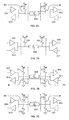
- Fig. 5A is a circuit diagram illustrating a DCI output driver circuit 501 that has a digitally controlled impedance Z. Impedance Z is selected to correspond with the impedance Z 0 of a line 502 located between the DCI driver circuit 501 and a receiver circuit 503.
- DCI circuit 201 is bypassed, such that some or all of the p-channel transistors 211 are turned on to provide a logic high output signal, and some or all of the n-channel transistors 212 are turned on to provide a logic low output signal.
- Fig. 5B is a circuit diagram illustrating an output driver circuit 504 in which DCI circuit 201 has been bypassed. Although output driver circuit 504 will exhibit an impedance, this impedance is not controlled to have a particular correspondence with the impedance Z 0 of line 502.
- DCI circuit 201 can also be controlled to turn on user-selected p-channel transistors to provide a logic high output signal, and to turn on user-selected n-channel transistors to provide a logic low output signal.
- DCI circuit 201 can be controlled to turn on only the coarse p-channel transistors P11-P15 to provide a logic high output signal, and to turn on only the coarse n-channel transistors N11-N15 to provide a logic low output signal, regardless of the external impedance Z 0 .
- This alternative is described in more detail in commonly owned, co-pending U.S. Patent No. 5,887,632, which is hereby incorporated by reference.
- DCI circuit 201 can be controlled to provide a transmission line termination resistance. As illustrated in Fig. 6A, it is common to provide external termination resistors 601-602, which are coupled between the ends of line 502 and a V CC supply voltage terminal. In Fig. 6A, output driver circuit 501 is coupled to an input buffer 513 at one end of line 502, thereby providing an input/output I/O configuration. Similarly, input buffer 503 is coupled to output driver circuit 511 at the other end of line 502.
- termination resistors 611 and 612 can be implemented using the digitally controlled impedance of output driver circuits 501 and 511, respectively, thereby eliminating the need for external termination resistors 601 and 602.
- the DCI circuits in output driver circuits 501 and 511 are referenced to a known resistance in response to reference voltages V PREF and V NREF having values of approximately V CC /2 and V CC /2, respectively.
- the termination resistance is controlled with respect to external reference resistors and can be adjusted for changes in temperature, voltage and/or process.
- a user-selected set of p-channel transistors is used to drive a logic high output signal.
- the coarse p-channel transistors P11-P15 may be selected to drive a logic high output signal in response to a corresponding input data signal.
- a subset of the fine p-channel transistors P1-P7 is selected to provide the termination resistance. While the coarse p-channel transistors are only turned on to drive a logic high output signal, the selected subset of the fine p-channel transistors P1-P7 are turned on at all times to provide the desired termination resistance. In other embodiments, other combinations of coarse and fine transistors can be used to serve as the user-selected transistors and the termination transistors.
- Fig. 6B illustrates a signal D1 being driven from output driver 511 to input buffer 513.
- output driver 511 is configured in manner described above. That is, output driver 511 provides logic high and low output signals by turning on user-selected transistors (e.g., all coarse p-channel transistors or all coarse n-channel transistors).
- a second set of p-channel transistors in driver circuit 511 are turned on to implement termination resistor 612.
- a tri-state signal applied to output driver circuit 501 is asserted, such that this output driver circuit 501 is not responsive to signals applied to its input terminal.
- the set of p-channel transistors in output driver circuit 501 that have been selected to implement termination resistor 611 remain turned on. As a result, the desired termination resistances 611 and 612 are provided between line 502 and the V CC supply terminal.
- Fig. 6C illustrates a signal D2 being driven from output driver 501 to input buffer 503.
- output driver 501 is configured in the same manner as output driver circuit 511 of Fig. 6B, such that this output driver 501 provides logic high and low output signals by turning on user-selected transistors, and provides the termination resistor 611 by turning on the set of p-channel transistors that have been selected to implement this termination resistor.
- a tri-state signal applied to output driver circuit 511 is asserted, such that this output driver circuit 511 is not responsive to signals applied to its input terminal.
- the set of p-channel transistors in output driver circuit 511 that have been selected to implement termination resistor 612 remain turned on.
- the desired termination resistances 611 and 612 are provided between line 502 and the V CC supply terminal.
- output driver circuits 501 and 511 provide termination resistances 611 and 612, respectively, for bi-directional signal transfer on line 502.
- the terminations illustrated in Figs. 6B-6C are referred to as single terminations, because a single set of transistors is used to provide each termination.
- termination resistors 711-712 and 713-714 can be implemented using the DCI circuits of driver circuits 501 and 511, respectively, thereby eliminating the need for external termination resistors 701 and 702 and the V CC /2 power supply.
- Each of resistors 711-714 is determined to have a resistance that is equal to twice the resistance of resistor 701 (or 702).
- resistors 711-712 and 713-714 are the Thevenin equivalents of resistors 701 and 702, respectively.
- the DCI circuits in output driver circuits 501 and 511 are referenced to known resistances in response to reference voltages V PREF and V NREF having values of approximately 2V CC /5 and 3V CC /5, respectively.
- impedance is controlled with respect to external reference resistors and can be adjusted for changes in temperature, voltage and/or process.
- Fig. 7B illustrates a signal D1 being driven from output driver 511 to input buffer 513.
- output driver 511 is configured in the same manner as output driver circuit 511 of Fig. 6B, such that this output driver 511 provides logic high and low output signals by turning on user-selected transistors, and provides termination resistances 713 and 714 by turning on the p-channel and n-channel transistors that have been determined to provide these desired termination resistances 713 and 714.
- a tri-state signal applied to output driver circuit 501 is asserted, such that this output driver circuit 501 is not responsive to signals applied to its input terminal.
- output driver circuit 501 provides the equivalent of termination resistance 701 coupled between line 502 and a V CC /2 supply terminal.
- output driver circuit 511 provides the equivalent of termination resistance 702 between line 502 and a V CC /2 supply terminal.
- Fig. 7C illustrates a signal D2 being driven from output driver 501 to input buffer 503.
- output driver 501 is configured in the same manner as output driver circuit 511 of Fig. 7B
- output driver 511 is configured in the same manner as output driver circuit 501 of Fig. 7B.
- output driver circuits 501 and 511 provide termination resistances 711-712 and 713-714, respectively, for bi-directional signal transfer on line 502.
- the terminations illustrated in Figs. 7B-7C are referred to as split terminations, because two sets of transistors are required to provide each termination.
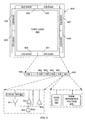
- Fig. 8 is a block diagram of an integrated circuit chip 800, which implements one embodiment of the present invention.
- IC chip 800 includes eight input/output block (IOB) banks 801-808 and core logic 810.
- IOB banks 801-808 are substantially identical.
- core logic 810 includes an array of configurable logic blocks and programmable interconnect circuitry.
- IOB banks 801-808 provide an interface between core logic 810 and circuitry external to chip 800.
- IOB bank 801 includes a plurality of IOBs 901-905 and a bank impedance control (BIC) circuit 910.
- BIC bank impedance control
- IOB 901 includes output driver circuit 911, comparator 921, input buffer circuit 931, I/O pad 941 and local digitally controlled impedance (DCI) circuit 961.
- bank impedance control circuit 910 includes a bank digitally controlled impedance (DCI) circuit 960 and bank reference voltage generator 970.
- bank reference voltage generator 970 provides the reference voltages that are used by IOBs 901-905. Thus, bank reference voltage generator 970 performs the functions of reference voltage circuits 311 and 411 (Figs. 3 and 4).
- bank impedance control circuit 910 In another embodiment, only one bank impedance control circuit 910 is provided for the entire chip 800. In this embodiment, bank impedance control circuit 910 provides the necessary control for all of the local DCI circuits on chip 800. In another embodiment, there are multiple bank impedance control circuits, which are capable of controlling one or more IOB banks.
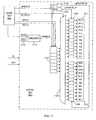
- Fig. 9 is a circuit diagram illustrating selected portions of IOB bank 801, including bank impedance control circuit 910 and IOBs 901-904. Note that the input buffer circuits (e.g., input buffer circuit 931) are not shown in Fig. 9 for purposes of clarity. IOBs 901-904 include respective local DCI circuits 961-964, respective output driver circuits 911-914, respective comparators 921-924 and respective I/O pads 941-944. Each of output driver circuits 911-914 includes a set of p-channel transistors 211 and a set of n-channel transistors 212, as described above in connection with Figs. 2-4.
- Reference voltage generator 970 provides the n-channel reference voltage, V NREF , and the p-channel reference voltage V PREF , on lines that extend through IOB bank 801.
- the comparator in every odd numbered IOB (e.g., 901, 903, 905) in IOB bank 801 is coupled to receive the V PREF voltage.
- the comparator in every even numbered IOB (e.g., 902, 904) in IOB bank 801 is 'coupled to receive the V NREF voltage.
- the output terminals of the comparators in odd numbered IOBs are coupled to programmable connections (e.g., 951, 953), which if programmed, will connect a corresponding comparator to a common HI_LO_P line.
- the output terminals of the comparators in even numbered IOBs are coupled to programmable connections (e.g., 952, 954), which if programmed, will connect a corresponding comparator to a common HI_LO_N line.
- the HI_LO_P line and the HI_LO_N line are routed to bank DCI circuit 960.
- Bank DCI circuit 960 also provides control signals to local DCI circuits 961-964. These control signals will be described in more detail below.
- IOB bank 801 operates as follows. One of the odd-numbered IOBs is selected to be a p-channel reference circuit, and one of the even-numbered IOBs is selected to be an n-channel reference circuit. This selection is made by setting a configuration memory bit in the local DCI circuit of each of these IOBs, and programming the connection to couple the output terminals of the comparators of these IOBs to the HI_LO_N and HI_LO_P lines. Although any one of the odd-numbered IOBs can be selected to be the p-channel reference circuit, IOB 901 is selected in the described embodiment.
- a configuration memory bit in local DCI circuit 961 is set, and programmable connection 951 is enabled.
- IOB 902 is selected in the described embodiment.
- a configuration memory bit in local DCI circuit 962 is set, and programmable connection 952 is enabled.
- IOB 901 is to serve as the p-channel reference circuit, a predetermined reference resistance R PREF is connected between pad 941 and the ground terminal in the manner illustrated in Fig. 3.
- R PREF a predetermined reference resistance connected between pad 941 and the ground terminal in the manner illustrated in Fig. 3.
- IOB 901 is configured in substantially the same manner illustrated in Fig. 3, except that the DCI circuit 201 of Fig. 3 has been divided into bank DCI circuit 960 and local DCI circuit 961.
- IOB 902 is to serve as the n-channel reference circuit, a predetermined reference resistance R NREF is connected between pad 942 and an external V CC supply terminal in the manner illustrated in Fig. 4.
- IOB 902 is configured in substantially the same manner illustrated in Fig. 4, except that the DCI circuit 201 of Fig. 4 has been divided into bank DCI circuit 960 and local DCI circuit 962.
- IOB bank 801 operates as follows.
- P-channel reference circuit 901 and n-channel reference circuit 902 are initially set to have predetermined turned-on p-channel and n-channel transistors.
- bank DCI circuit 960 processes the HI_LO_P signal provided by p-channel reference circuit 901.
- bank DCI circuit 960 instructs local DCI circuit 961 to enable/disable the p-channel transistors in driver circuit 911 in the manner described above in connection with Fig. 3.
- bank DCI circuit 960 also instructs other local DCI circuits to enable/disable the same p-channel transistors as local DCI circuit 961.
- local DCI circuits 963-964 when logic low data signals D3-D4 are applied to local DCI circuits 963-964, these local DCI circuits will enable the same p-channel transistors determined by the p-channel reference circuit 901. For example, if bank DCI circuit 960 instructs local DCI circuit 961 in the p-channel reference circuit 901 to enable fine p-channel transistors P1-P4 and coarse p-channel transistor P14, then bank DCI circuit 960 will similarly instruct local DCI circuit 963 to enable fine p-channel transistors P1-P4 and coarse p-channel transistor P14 when data signal D3 has a logic low value.
- bank DCI circuit 960 processes the HI_LO_N signal provided by n-channel reference circuit 902. In response, bank DCI circuit 960 instructs local DCI circuit 962 to enable/disable the n-channel transistors in driver circuit 912 in the manner described above in connection with Fig. 4. Bank DCI circuit 960 also instructs other local DCI circuits to enable/disable the same n-channel transistors as local DCI circuit 962.
- bank DCI circuit 960 instructs local DCI circuit 962 in the n-channel reference circuit 902 to enable fine n-channel transistors N1-N2 and coarse n-channel transistor N13
- bank DCI circuit 960 will similarly instruct local DCI circuit 963 to enable fine n-channel transistors N1-N2 and coarse n-channel transistor N13 when data signal D3 has a logic high value.
- the IOB 904 can be configured in a manner different than IOB 903.
- output driver circuit 913 of IOB 903 can be configured in response to different reference voltages (V NREF and V PREF ) than output driver circuit 914 of IOB 904.
- V NREF and V PREF reference voltages
- output driver circuit 913 will exhibit different resistances than output driver circuit 914. This is accomplished by providing different sets of reference voltages with reference voltage supply 970.
- Reference voltage supply 970 can be controlled to provide different reference voltages V PREF and V NREF at different times. For example, reference voltage supply 970 can be controlled to provide a first set of reference voltages that are used by p-channel and n-channel reference circuits 901 and 902 to determine the appropriate p-channel and n-channel transistors to be enabled within IOB 903. Reference voltage supply 970 can also be controlled to provide a second set of reference voltages that are used by p-channel and n-channel reference circuits 901 and 902 to determine the appropriate p-channel and n-channel transistors to be enabled within IOB 904. In the described embodiment, reference voltage supply 970 can be controlled to provide up to four sets of reference voltages.
- Bank DCI circuit 960 is able to address the local DCI circuits 961-964, such that the appropriate information is provided to the appropriate IOBs.
- Fig. 10 is a circuit diagram of reference voltage supply 970 in accordance with one embodiment of the present invention.
- Reference voltage supply 970 includes p-channel reference voltage generator 1010, n-channel reference voltage generator 1020 and decoder circuit 1030.
- P-channel reference voltage generator 1010 includes transmission gates 1001-1004, resistors 1011-1014 and n-channel transistor 1021. Resistors 1011, 1012, 1013 and 1014 have relative resistances of 8R, 4R, 12R and 8R, respectively.
- N-channel reference voltage generator 1020 includes transmission gates 1005-1008, resistors 1015-1018, n-channel transistors 1022-1023 and p-channel transistor 1024.
- Resistors 1015, 1016, 1017 and 1018 have relative resistances of 8R, 8R, 4R and 12R, respectively.
- Decoder circuit receives address signals a[2:0] from bank DCI circuit 960, and in response, provides control signals to transmission gates 1001-1008 and transistors 1021-1023.
- Table 1 summarizes the status of transmission gates 1001-1004, transistor 1021 and the p-channel reference voltage V PREF for the various address signals a[2:0].
- Table 2 summarizes the status of transmission gates 1005-1008, transistor 1022-1024 and the n-channel reference voltage V NREF for the various address signals a[2:0].
- a[2:0] 1005 1022 1006 1007 1008 1023 1024
- V NREF 000 101 110 111 OFF OFF OFF ON 0 001 ON ON OFF OFF OFF V CC /2 010 ON OFF ON OFF OFF V CC /3 011 ON ON OFF OFF OFF V CC /2 100 ON OFF OFF ON OFF 3V CC /5
- Addresses of "001" or “010” are used to provide DCI output driver circuits with different impedances (Fig. 5A).
- An address of "011” is used to provide a single termination pull-up to V CC (Fig. 6B).
- An address of "100” is used to provide a split termination to V CC and ground (Fig. 7B).
- Fig. 11 is a block diagram illustrating bank DCI circuit 960 and local DCI circuit 963 in more detail. Local DCI circuits 961-962 and 964 are identical to local DCI circuit 963.
- Local DCI circuit 963 includes shift register 1101, data decoder 1102, p-channel register 1103, n-channel register 1104, configuration memory cells 1110, address decoder 1111 and logical AND gates 1121-1122.
- Bank DCI circuit 660 and local DCI circuit 663 operate as follows in accordance with one embodiment of the present invention.
- Configuration memory cells 1110 store four configuration bits. One of these configuration bits indicates whether IOB 903 will serve as a reference IOB. If this configuration bit is set, then address decoder 1111 will assert an ENABLE signal regardless of the state of the applied address signal a[2:0]. The remaining three configuration bits identify a "type" of the output driver circuit 913 (assuming that IOB 903 is not a reference IOB). There are five “types" of output driver circuits in accordance with the described embodiment. Table 3 defines the reference voltages used for each of the five types. Note that the contents of configuration memory cells 1110 will correspond with one of the address signals a[2:0].
- Type Configuration Memory Cells 1110 V PREF V NREF 000, 101, 110, 111 0 0 001 V CC /2 V CC /2 010 V CC /3 2V CC /3 011 V CC /2 V CC /2 100 3V CC /5 2V CC /5
- address decoder 1111 will assert an ENABLE signal, thereby enabling shift register 1101.
- shift register 1101 will sequentially shift in the DATA signal provided by bank DCI circuit 960.
- the DATA signal identifies the p-channel transistors 211 or the n-channel transistors 212 to be turned on during the present iteration.
- Shift register 1101 provides the loaded DATA values to data decoder 1102.
- Bank DCI circuit 960 initially provides a N_OR_P signal having a logic "0" value.
- data decoder 1102 will decode the contents of shift register 1101, and transmit the results to p-channel register 1103.
- Bank DCI circuit 960 then asserts a logic high UPDATE signal, which causes AND gate 1121 to assert a logic high UPDATE_P signal.
- p-channel register 1103 loads the results provided by data decoder 1102. The contents of p-channel register 1103 are then used to control p-channel transistors P1-P7 and P11-P15 in the manner described above.
- Data decoder 1102 operates as follows. Data decoder receives the 8-bit signal D[7:0] received from shift register 1101.
- the D[7:0] signal includes five bits D[7:3] to control coarse transistors (i.e., coarse p-channel transistors P11-P15 or coarse n-channel transistors N11-N15). These five bits D[7:3] are routed directly through decoder 1102 to either register 1103 or 1104 in response to the N_OR_P signal.
- the D[7:0] signal also includes three bits D[2:0] to control fine transistors (i.e., fine p-channel transistors P1-P7 or fine n-channel transistors N1-N7). Decoder 1102 provides signals that will turn on 0 to 7 of the fine transistors in response to the D[2:0] bits.
- IOB bank 801 The operation of IOB bank 801 will now be summarized. First, one of IOBs 901-905 is configured as a p-channel reference circuit, and another one of IOBs 901-905 is configured as an n-channel reference circuit. The remaining IOBs are configured to have a particular 'type' (e.g., a first type, a second type, etc.) by appropriately programming the configuration memory cells 1110 within the IOBs.
- a particular 'type' e.g., a first type, a second type, etc.
- Bank DCI circuit 960 then asserts a first address signal a 1 [2:0] (e.g., "001") and a first data signal D 1 [7:0].
- the first address signal a 1 [2:0] causes reference voltage circuit 970 to generate a first pair of reference voltages V PREF1 and V NREF1 (e.g., V CC /2 and V CC /2).
- the first data signal D 1 [7:0] which identifies p-channel transistors to be enabled, is latched into the p-channel reference IOB.
- the first address signal a 1 [2:0] also causes the first data signal D 1 [7:0] to be latched into all of the IOBs of the first type.
- the bank DCI circuit 960 then provides a logic low N_OR_P signal and a logic high UPDATE signal, thereby causing the first data signal D 1 [7:0] to be decoded and used to control the p-channel transistors in both the p-channel reference circuit and the IOBs of the first type.
- the p-channel reference circuit provides a HI_LO_P signal having a logic high or low value to bank DCI circuit 960. This process is repeated until the p-channel reference circuit has provided the desired p-channel settings to all of the IOBs of the first type.
- the address signal a[2:0] is then incremented to the second type ("010"), such that the reference voltage circuit 970 generates a second pair of reference voltages.
- the p-channel reference circuit is used to provide the desired p-channel settings to all of the IOBs of the second type.
- This process is repeated such that the desired p-channel settings are provided for all of the different types of IOBs.
- the n-channel reference circuit is then used to provide the desired n-channel settings for the different types of IOBs.
- bank DCI circuit 960 asserts the first address signal a 1 [2:0] and then provides a data signal D 2 [7:0].
- This data signal D 2 [7:0] which identifies n-channel transistors to be enabled, is latched into the n-channel reference circuit.
- the first address signal a 1 [2:0] also enables the second data signal D 2 [7:0] to be latched into all of the IOBs of the first type.
- the bank DCI circuit 960 then provides a logic high N_OR_P signal and a logic high UPDATE signal, thereby causing the data signal D 2 [7:0] to be decoded and used to control the n-channel transistors in both the n-channel reference circuit and the IOBs of the first type.
- the n-channel reference IOB provides a HI_LO_N signal having a logic high or low value to bank DCI circuit 960. This process is repeated until the n-channel reference circuit has provided the desired n-channel settings to all of the IOBs of the first type.
- the address signal a [2:0] is then incremented to the second type ("010"), such that the reference voltage circuit 970 generates a second pair of reference voltages.
- the n-channel reference circuit is used to provide the desired n-channel settings to all of the IOBs of the second type.
- This process is repeated such that the desired n-channel settings are provided for all of the different types of IOBs.
- the process then repeats, with the p-channel transistor settings being updated for the various types, and then the n-channel transistor settings being updated for the various types. In this manner, the p-channel and n-channel determinations are continuously being updated for each type during operation of the chip.
- IOBs can be excluded from this process by programming the configuration memory cells 1110 to store a 3-bit value of "000”, “101", “110” or "111".
- the p-channel and n-channel transistors to be enabled are determined by the user programming configuration memory cells.
- n-channel transistors have been used as pull-up elements
- n-channel transistors have been used as pull-down elements
- n-channel transistors can be used as pull-up elements
- p-channel transistors can be used as pull-down elements in other embodiments.
Landscapes
- Engineering & Computer Science (AREA)
- Computing Systems (AREA)
- Mathematical Physics (AREA)
- General Engineering & Computer Science (AREA)
- Physics & Mathematics (AREA)
- Computer Hardware Design (AREA)
- Signal Processing (AREA)
- Computer Networks & Wireless Communication (AREA)
- Power Engineering (AREA)
- Logic Circuits (AREA)
- Semiconductor Integrated Circuits (AREA)
- Design And Manufacture Of Integrated Circuits (AREA)
- Networks Using Active Elements (AREA)
Applications Claiming Priority (3)
| Application Number | Priority Date | Filing Date | Title |
|---|---|---|---|
| US684539 | 1991-04-11 | ||
| US09/684,539 US6445245B1 (en) | 2000-10-06 | 2000-10-06 | Digitally controlled impedance for I/O of an integrated circuit device |
| EP01912822A EP1330875B1 (de) | 2000-10-06 | 2001-02-16 | Digitalgesteuerte impedanz für eingangs/ausgangsschaltung einer integrierten schaltungsvorrichtung |
Related Parent Applications (2)
| Application Number | Title | Priority Date | Filing Date |
|---|---|---|---|
| EP01912822A Division EP1330875B1 (de) | 2000-10-06 | 2001-02-16 | Digitalgesteuerte impedanz für eingangs/ausgangsschaltung einer integrierten schaltungsvorrichtung |
| EP01912822.2 Division | 2001-02-16 |
Publications (2)
| Publication Number | Publication Date |
|---|---|
| EP1515442A1 true EP1515442A1 (de) | 2005-03-16 |
| EP1515442B1 EP1515442B1 (de) | 2010-05-05 |
Family
ID=24748466
Family Applications (2)
| Application Number | Title | Priority Date | Filing Date |
|---|---|---|---|
| EP01912822A Expired - Lifetime EP1330875B1 (de) | 2000-10-06 | 2001-02-16 | Digitalgesteuerte impedanz für eingangs/ausgangsschaltung einer integrierten schaltungsvorrichtung |
| EP04023919A Expired - Lifetime EP1515442B1 (de) | 2000-10-06 | 2001-02-16 | Digitalgesteuerte Impedanz für Eingangs-/Ausgangsschaltung einer integrierten Vorrichtung |
Family Applications Before (1)
| Application Number | Title | Priority Date | Filing Date |
|---|---|---|---|
| EP01912822A Expired - Lifetime EP1330875B1 (de) | 2000-10-06 | 2001-02-16 | Digitalgesteuerte impedanz für eingangs/ausgangsschaltung einer integrierten schaltungsvorrichtung |
Country Status (6)
| Country | Link |
|---|---|
| US (2) | US6445245B1 (de) |
| EP (2) | EP1330875B1 (de) |
| JP (1) | JP4963774B2 (de) |
| CA (1) | CA2425056C (de) |
| DE (2) | DE60133400T2 (de) |
| WO (1) | WO2002031979A1 (de) |
Families Citing this family (75)
| Publication number | Priority date | Publication date | Assignee | Title |
|---|---|---|---|---|
| US6773908B1 (en) * | 1992-10-30 | 2004-08-10 | Iowa State University Research Foundation, Inc. | Proteins encoded by polynucleic acids of porcine reproductive and respiratory syndrome virus (PRRSV) |
| JP4657497B2 (ja) * | 2001-06-07 | 2011-03-23 | ルネサスエレクトロニクス株式会社 | 可変インピーダンス回路 |
| FR2825802B1 (fr) * | 2001-06-12 | 2004-01-23 | St Microelectronics Sa | Dispositif de comparaison de deux resistances et systeme de compensation des resistances integrees l'incorporant |
| US6798237B1 (en) | 2001-08-29 | 2004-09-28 | Altera Corporation | On-chip impedance matching circuit |
| US6657906B2 (en) * | 2001-11-28 | 2003-12-02 | Micron Technology, Inc. | Active termination circuit and method for controlling the impedance of external integrated circuit terminals |
| US6812732B1 (en) | 2001-12-04 | 2004-11-02 | Altera Corporation | Programmable parallel on-chip parallel termination impedance and impedance matching |
| US6836144B1 (en) | 2001-12-10 | 2004-12-28 | Altera Corporation | Programmable series on-chip termination impedance and impedance matching |
| US6812734B1 (en) | 2001-12-11 | 2004-11-02 | Altera Corporation | Programmable termination with DC voltage level control |
| US7109744B1 (en) | 2001-12-11 | 2006-09-19 | Altera Corporation | Programmable termination with DC voltage level control |
| US7093041B2 (en) * | 2001-12-20 | 2006-08-15 | Lsi Logic Corporation | Dual purpose PCI-X DDR configurable terminator/driver |
| EP1376863B1 (de) * | 2002-05-08 | 2008-03-19 | NEC Electronics Corporation | Verfahren und Schaltungsanordnung zur Erzeugung eines Steuersignals zur Impedanzanpassung |
| US20030214342A1 (en) * | 2002-05-14 | 2003-11-20 | Darrin Benzer | IO clamping circuit method utilizing output driver transistors |
| JP4212309B2 (ja) * | 2002-07-01 | 2009-01-21 | 株式会社ルネサステクノロジ | 半導体集積回路 |
| US6836142B2 (en) * | 2002-07-12 | 2004-12-28 | Xilinx, Inc. | Asymmetric bidirectional bus implemented using an I/O device with a digitally controlled impedance |
| US6963218B1 (en) * | 2002-08-09 | 2005-11-08 | Xilinx, Inc. | Bi-directional interface and communication link |
| US6967500B1 (en) * | 2002-11-27 | 2005-11-22 | Lattice Semiconductor Corporation | Electronic circuit with on-chip programmable terminations |
| US6933746B1 (en) | 2003-05-21 | 2005-08-23 | Planet Ate, Inc. | Method and apparatus for coupling an input node to an output node |
| US6922077B2 (en) * | 2003-06-27 | 2005-07-26 | Intel Corporation | Hybrid compensated buffer design |
| US6888369B1 (en) | 2003-07-17 | 2005-05-03 | Altera Corporation | Programmable on-chip differential termination impedance |
| US6909305B1 (en) | 2003-08-08 | 2005-06-21 | Ami Semiconductor, Inc. | Digitally controlled impedance driver matching for wide voltage swings at input/output node and having programmable step size |
| US6859064B1 (en) | 2003-08-20 | 2005-02-22 | Altera Corporation | Techniques for reducing leakage current in on-chip impedance termination circuits |
| US6888370B1 (en) | 2003-08-20 | 2005-05-03 | Altera Corporation | Dynamically adjustable termination impedance control techniques |
| JP4450605B2 (ja) * | 2003-11-14 | 2010-04-14 | 株式会社ルネサステクノロジ | 半導体装置 |
| US7095245B2 (en) * | 2003-11-14 | 2006-08-22 | Intel Corporation | Internal voltage reference for memory interface |
| US7019553B2 (en) * | 2003-12-01 | 2006-03-28 | Micron Technology, Inc. | Method and circuit for off chip driver control, and memory device using same |
| US7741866B2 (en) * | 2003-12-23 | 2010-06-22 | Nxp B.V. | Load-aware circuit arrangement |
| US7321613B2 (en) * | 2003-12-31 | 2008-01-22 | Intel Corporation | Automatic impedance matching compensation for a serial point to point link |
| US7138868B2 (en) * | 2004-08-11 | 2006-11-21 | Texas Instruments Incorporated | Method and circuit for trimming a current source in a package |
| US7355453B2 (en) * | 2004-08-11 | 2008-04-08 | Altera Corporation | Techniques for trimming drive current in output drivers |
| DE102004044422B3 (de) * | 2004-09-14 | 2006-03-30 | Infineon Technologies Ag | Kalibrierungsschaltung für eine Treibersteuerschaltung und Treibersteuerschaltung |
| US7218155B1 (en) | 2005-01-20 | 2007-05-15 | Altera Corporation | Techniques for controlling on-chip termination resistance using voltage range detection |
| US7221193B1 (en) | 2005-01-20 | 2007-05-22 | Altera Corporation | On-chip termination with calibrated driver strength |
| US7489173B1 (en) | 2005-02-18 | 2009-02-10 | Xilinx, Inc. | Signal adjustment for duty cycle control |
| US7215579B2 (en) * | 2005-02-18 | 2007-05-08 | Micron Technology, Inc. | System and method for mode register control of data bus operating mode and impedance |
| US8618866B2 (en) * | 2005-04-29 | 2013-12-31 | Ati Technologies Ulc | Apparatus and methods for balancing supply voltages |
| US7389194B2 (en) * | 2005-07-06 | 2008-06-17 | Rambus Inc. | Driver calibration methods and circuits |
| US7679397B1 (en) | 2005-08-05 | 2010-03-16 | Altera Corporation | Techniques for precision biasing output driver for a calibrated on-chip termination circuit |
| US8222917B2 (en) * | 2005-11-03 | 2012-07-17 | Agate Logic, Inc. | Impedance matching and trimming apparatuses and methods using programmable resistance devices |
| US7391229B1 (en) | 2006-02-18 | 2008-06-24 | Altera Corporation | Techniques for serially transmitting on-chip termination control signals |
| KR100738961B1 (ko) * | 2006-02-22 | 2007-07-12 | 주식회사 하이닉스반도체 | 반도체 메모리의 출력 드라이빙 장치 |
| US7420386B2 (en) | 2006-04-06 | 2008-09-02 | Altera Corporation | Techniques for providing flexible on-chip termination control on integrated circuits |
| US20080018357A1 (en) * | 2006-07-18 | 2008-01-24 | Honeywell International Inc. | Automatic termination circuit |
| US7417452B1 (en) | 2006-08-05 | 2008-08-26 | Altera Corporation | Techniques for providing adjustable on-chip termination impedance |
| KR100782328B1 (ko) * | 2006-08-11 | 2007-12-06 | 삼성전자주식회사 | 페일 세이프 io 회로를 구비하는 반도체 집적회로 장치및 이를 포함하는 전자 기기 |
| US7423450B2 (en) * | 2006-08-22 | 2008-09-09 | Altera Corporation | Techniques for providing calibrated on-chip termination impedance |
| JP4199789B2 (ja) * | 2006-08-29 | 2008-12-17 | エルピーダメモリ株式会社 | 半導体装置の出力回路調整方法 |
| KR100780646B1 (ko) * | 2006-10-31 | 2007-11-30 | 주식회사 하이닉스반도체 | 온 다이 터미네이션 장치 및 이를 포함하는 반도체장치. |
| US7372295B1 (en) | 2006-12-22 | 2008-05-13 | Altera Corporation | Techniques for calibrating on-chip termination impedances |
| US7443193B1 (en) | 2006-12-30 | 2008-10-28 | Altera Corporation | Techniques for providing calibrated parallel on-chip termination impedance |
| TW200910373A (en) | 2007-06-08 | 2009-03-01 | Mosaid Technologies Inc | Dynamic impedance control for input/output buffers |
| US20090009212A1 (en) * | 2007-07-02 | 2009-01-08 | Martin Brox | Calibration system and method |
| JP5059580B2 (ja) * | 2007-12-20 | 2012-10-24 | ルネサスエレクトロニクス株式会社 | 終端回路 |
| US8065570B1 (en) * | 2008-01-28 | 2011-11-22 | Xilinx, Inc. | Testing an integrated circuit having configurable input/output terminals |
| US7999530B2 (en) | 2008-03-21 | 2011-08-16 | Intersil Americas Inc. | Device under test power supply |
| US20100164471A1 (en) * | 2008-12-30 | 2010-07-01 | M2000 | Calibration of programmable i/o components using a virtual variable external resistor |
| US8072242B2 (en) * | 2009-12-18 | 2011-12-06 | Meta Systems | Merged programmable output driver |
| US7973553B1 (en) | 2010-03-11 | 2011-07-05 | Altera Corporation | Techniques for on-chip termination |
| FR2960720A1 (fr) * | 2010-05-25 | 2011-12-02 | St Microelectronics Sa | Procede de protection d'un circuit logique contre des radiations externes et dispositif electronique associe. |
| US8222918B1 (en) | 2010-09-21 | 2012-07-17 | Xilinx, Inc. | Output driver and method of operating the same |
| US8018250B1 (en) | 2010-10-19 | 2011-09-13 | Xilinx, Inc. | Input/output block and operation thereof |
| US8570064B1 (en) * | 2011-11-11 | 2013-10-29 | Altera Corporation | Methods and systems for programmable implementation of on-chip termination calibration |
| US8786990B2 (en) * | 2012-04-04 | 2014-07-22 | Globalfoundries Singapore Pte. Ltd. | Driver-based distributed multi-path ESD scheme |
| FR2991501A1 (fr) | 2012-05-30 | 2013-12-06 | Stmicroelectronic Sa | Circuit integre comportant au moins un port digital de sortie d'impedance reglable, et procede de reglage correspondant |
| US9000800B1 (en) | 2012-09-17 | 2015-04-07 | Xilinx, Inc. | System and method of eliminating on-board calibration resistor for on-die termination |
| US8766701B1 (en) * | 2013-03-08 | 2014-07-01 | Xilinx, Inc. | Analog multiplexing with independent power supplies |
| KR20140129917A (ko) * | 2013-04-30 | 2014-11-07 | 인텔렉추얼디스커버리 주식회사 | 무선 전력 전송 장치 및 무선 전력 전송 방법 |
| US9444455B2 (en) * | 2013-12-10 | 2016-09-13 | Sandisk Technologies Llc | Load impedance adjustment for an interface of a data storage device |
| US9369128B1 (en) | 2014-08-15 | 2016-06-14 | Altera Corporation | Circuits and methods for impedance calibration |
| US9935597B2 (en) | 2016-05-27 | 2018-04-03 | Xilinx, Inc. | Circuit for and method of receiving an input signal |
| US9647663B1 (en) | 2016-06-27 | 2017-05-09 | Altera Corporation | Differential input buffer circuits and methods |
| US9712257B1 (en) | 2016-08-12 | 2017-07-18 | Xilinx, Inc. | Digitally-controlled impedance control for dynamically generating drive strength for a transmitter |
| US10063232B1 (en) | 2017-09-13 | 2018-08-28 | Xilinx, Inc. | Digitally controlled impedance calibration for a driver using an on-die reference resistor |
| US20230238958A1 (en) * | 2022-01-26 | 2023-07-27 | Mediatek Inc. | Integrated circuit device and chip device |
| US12206397B2 (en) * | 2022-09-21 | 2025-01-21 | Apple Inc. | Power switching circuitry with feedback control |
| US20240291488A1 (en) * | 2023-02-27 | 2024-08-29 | Stmicroelectronics International N.V. | Voltage compensation of differential voltage swing |
Citations (3)
| Publication number | Priority date | Publication date | Assignee | Title |
|---|---|---|---|---|
| EP0978943A2 (de) * | 1998-07-31 | 2000-02-09 | Hewlett-Packard Company | Kalibrierungsschaltung |
| US6054881A (en) * | 1998-01-09 | 2000-04-25 | Advanced Micro Devices, Inc. | Input/output (I/O) buffer selectively providing resistive termination for a transmission line coupled thereto |
| US6087847A (en) * | 1997-07-29 | 2000-07-11 | Intel Corporation | Impedance control circuit |
Family Cites Families (14)
| Publication number | Priority date | Publication date | Assignee | Title |
|---|---|---|---|---|
| US5287536A (en) * | 1990-04-23 | 1994-02-15 | Texas Instruments Incorporated | Nonvolatile memory array wordline driver circuit with voltage translator circuit |
| US5134311A (en) | 1990-06-07 | 1992-07-28 | International Business Machines Corporation | Self-adjusting impedance matching driver |
| US5463326A (en) | 1993-04-13 | 1995-10-31 | Hewlett-Packard Company | Output drivers in high frequency circuits |
| AU6820094A (en) * | 1993-05-13 | 1994-12-12 | Microunity Systems Engineering, Inc. | Bias voltage distribution system |
| JPH07142985A (ja) * | 1993-11-16 | 1995-06-02 | Mitsubishi Electric Corp | 出力回路 |
| JPH0832435A (ja) * | 1994-07-18 | 1996-02-02 | Hitachi Ltd | 半導体装置 |
| US5559441A (en) | 1995-04-19 | 1996-09-24 | Hewlett-Packard Company | Transmission line driver with self adjusting output impedance |
| JP3588953B2 (ja) * | 1997-02-03 | 2004-11-17 | 富士通株式会社 | 半導体集積回路装置 |
| JPH10290147A (ja) * | 1997-04-14 | 1998-10-27 | Mitsubishi Electric Corp | 遅延量可変回路 |
| JPH11195766A (ja) * | 1997-10-31 | 1999-07-21 | Mitsubishi Electric Corp | 半導体集積回路装置 |
| KR100266747B1 (ko) * | 1997-12-31 | 2000-09-15 | 윤종용 | 임피던스 조정 회로를 구비한 반도체 장치 |
| JP3944298B2 (ja) | 1998-02-16 | 2007-07-11 | 株式会社ルネサステクノロジ | 半導体集積回路 |
| US6232814B1 (en) * | 1998-11-10 | 2001-05-15 | Intel Corporation | Method and apparatus for controlling impedance on an input-output node of an integrated circuit |
| JP3849835B2 (ja) * | 1999-06-23 | 2006-11-22 | 株式会社ルネサステクノロジ | 半導体集積回路装置 |
-
2000
- 2000-10-06 US US09/684,539 patent/US6445245B1/en not_active Expired - Lifetime
-
2001
- 2001-02-16 WO PCT/US2001/005270 patent/WO2002031979A1/en not_active Ceased
- 2001-02-16 EP EP01912822A patent/EP1330875B1/de not_active Expired - Lifetime
- 2001-02-16 CA CA002425056A patent/CA2425056C/en not_active Expired - Lifetime
- 2001-02-16 DE DE60133400T patent/DE60133400T2/de not_active Expired - Lifetime
- 2001-02-16 EP EP04023919A patent/EP1515442B1/de not_active Expired - Lifetime
- 2001-02-16 JP JP2002535259A patent/JP4963774B2/ja not_active Expired - Lifetime
- 2001-02-16 DE DE60142091T patent/DE60142091D1/de not_active Expired - Lifetime
- 2001-11-30 US US10/007,167 patent/US6489837B2/en not_active Expired - Lifetime
Patent Citations (3)
| Publication number | Priority date | Publication date | Assignee | Title |
|---|---|---|---|---|
| US6087847A (en) * | 1997-07-29 | 2000-07-11 | Intel Corporation | Impedance control circuit |
| US6054881A (en) * | 1998-01-09 | 2000-04-25 | Advanced Micro Devices, Inc. | Input/output (I/O) buffer selectively providing resistive termination for a transmission line coupled thereto |
| EP0978943A2 (de) * | 1998-07-31 | 2000-02-09 | Hewlett-Packard Company | Kalibrierungsschaltung |
Also Published As
| Publication number | Publication date |
|---|---|
| WO2002031979A1 (en) | 2002-04-18 |
| US6445245B1 (en) | 2002-09-03 |
| DE60133400D1 (de) | 2008-05-08 |
| DE60142091D1 (de) | 2010-06-17 |
| JP2004511945A (ja) | 2004-04-15 |
| EP1330875A1 (de) | 2003-07-30 |
| EP1515442B1 (de) | 2010-05-05 |
| CA2425056C (en) | 2007-03-27 |
| CA2425056A1 (en) | 2002-04-18 |
| JP4963774B2 (ja) | 2012-06-27 |
| US20020101278A1 (en) | 2002-08-01 |
| DE60133400T2 (de) | 2009-04-23 |
| US6489837B2 (en) | 2002-12-03 |
| EP1330875B1 (de) | 2008-03-26 |
Similar Documents
| Publication | Publication Date | Title |
|---|---|---|
| EP1330875B1 (de) | Digitalgesteuerte impedanz für eingangs/ausgangsschaltung einer integrierten schaltungsvorrichtung | |
| US6836142B2 (en) | Asymmetric bidirectional bus implemented using an I/O device with a digitally controlled impedance | |
| US6963218B1 (en) | Bi-directional interface and communication link | |
| US6642740B2 (en) | Programmable termination circuit and method | |
| US5949254A (en) | Adjustable output driver circuit | |
| JP3948496B2 (ja) | 多重i/oスタンダードをサポートする入力/出力バッファ | |
| US5606275A (en) | Buffer circuit having variable output impedance | |
| JP4430175B2 (ja) | デジタル制御出力ドライバ及びインピーダンス整合方法 | |
| EP2412136B1 (de) | Spannungsgesteuerter sendeentzerrer | |
| US6605958B2 (en) | Precision on-chip transmission line termination | |
| US7675326B1 (en) | Dynamically-adjustable differential output drivers | |
| US6812734B1 (en) | Programmable termination with DC voltage level control | |
| US6710617B2 (en) | Variable slew rate control for open drain bus | |
| US5864584A (en) | Circuitry for allowing two drivers to communicate with two receivers using one transmission line | |
| US6972588B1 (en) | Adjustable differential input and output drivers | |
| US6509757B1 (en) | Binary weighted thermometer code for PVT controlled output drivers | |
| WO2002039685A2 (en) | Low-voltage differential receiver/transmitter and calibration method thereof | |
| US7109744B1 (en) | Programmable termination with DC voltage level control | |
| EP1247341B1 (de) | Programmierbare pufferschaltung | |
| US7400272B2 (en) | Hybrid binary/thermometer code for controlled-voltage integrated circuit output drivers | |
| US6967500B1 (en) | Electronic circuit with on-chip programmable terminations | |
| US20040201401A1 (en) | Bi-directional impedance matching circuit | |
| US6859066B1 (en) | Bank-based input/output buffers with multiple reference voltages | |
| US6930513B2 (en) | Simultaneous bi-directional signal transmission system and semiconductor device therefor |
Legal Events
| Date | Code | Title | Description |
|---|---|---|---|
| PUAI | Public reference made under article 153(3) epc to a published international application that has entered the european phase |
Free format text: ORIGINAL CODE: 0009012 |
|
| 17P | Request for examination filed |
Effective date: 20041102 |
|
| AC | Divisional application: reference to earlier application |
Ref document number: 1330875 Country of ref document: EP Kind code of ref document: P |
|
| AK | Designated contracting states |
Kind code of ref document: A1 Designated state(s): DE FR GB IE |
|
| RIN1 | Information on inventor provided before grant (corrected) |
Inventor name: BERGENDAHL, JASON R.,C/O XILINX, INC. Inventor name: SCHULTZ, DAVID P.,C/O XILINX, INC. Inventor name: MENON, SURESH M. Inventor name: HAO, EUNICE U. D. Inventor name: TAN, JIAN |
|
| AKX | Designation fees paid |
Designated state(s): DE FR GB IE |
|
| 17Q | First examination report despatched |
Effective date: 20060914 |
|
| GRAP | Despatch of communication of intention to grant a patent |
Free format text: ORIGINAL CODE: EPIDOSNIGR1 |
|
| GRAS | Grant fee paid |
Free format text: ORIGINAL CODE: EPIDOSNIGR3 |
|
| GRAA | (expected) grant |
Free format text: ORIGINAL CODE: 0009210 |
|
| AC | Divisional application: reference to earlier application |
Ref document number: 1330875 Country of ref document: EP Kind code of ref document: P |
|
| AK | Designated contracting states |
Kind code of ref document: B1 Designated state(s): DE FR GB IE |
|
| REG | Reference to a national code |
Ref country code: GB Ref legal event code: FG4D |
|
| REG | Reference to a national code |
Ref country code: IE Ref legal event code: FG4D |
|
| REF | Corresponds to: |
Ref document number: 60142091 Country of ref document: DE Date of ref document: 20100617 Kind code of ref document: P |
|
| PLBE | No opposition filed within time limit |
Free format text: ORIGINAL CODE: 0009261 |
|
| STAA | Information on the status of an ep patent application or granted ep patent |
Free format text: STATUS: NO OPPOSITION FILED WITHIN TIME LIMIT |
|
| 26N | No opposition filed |
Effective date: 20110208 |
|
| REG | Reference to a national code |
Ref country code: DE Ref legal event code: R097 Ref document number: 60142091 Country of ref document: DE Effective date: 20110207 |
|
| REG | Reference to a national code |
Ref country code: FR Ref legal event code: PLFP Year of fee payment: 16 |
|
| REG | Reference to a national code |
Ref country code: FR Ref legal event code: PLFP Year of fee payment: 17 |
|
| REG | Reference to a national code |
Ref country code: FR Ref legal event code: PLFP Year of fee payment: 18 |
|
| PGFP | Annual fee paid to national office [announced via postgrant information from national office to epo] |
Ref country code: IE Payment date: 20200227 Year of fee payment: 20 Ref country code: DE Payment date: 20200227 Year of fee payment: 20 Ref country code: GB Payment date: 20200227 Year of fee payment: 20 |
|
| PGFP | Annual fee paid to national office [announced via postgrant information from national office to epo] |
Ref country code: FR Payment date: 20200225 Year of fee payment: 20 |
|
| REG | Reference to a national code |
Ref country code: DE Ref legal event code: R071 Ref document number: 60142091 Country of ref document: DE |
|
| REG | Reference to a national code |
Ref country code: GB Ref legal event code: PE20 Expiry date: 20210215 |
|
| REG | Reference to a national code |
Ref country code: IE Ref legal event code: MK9A |
|
| PG25 | Lapsed in a contracting state [announced via postgrant information from national office to epo] |
Ref country code: IE Free format text: LAPSE BECAUSE OF EXPIRATION OF PROTECTION Effective date: 20210216 Ref country code: GB Free format text: LAPSE BECAUSE OF EXPIRATION OF PROTECTION Effective date: 20210215 |