EP1513161A2 - Halbleiter- Speicheranordnung - Google Patents
Halbleiter- Speicheranordnung Download PDFInfo
- Publication number
- EP1513161A2 EP1513161A2 EP04255263A EP04255263A EP1513161A2 EP 1513161 A2 EP1513161 A2 EP 1513161A2 EP 04255263 A EP04255263 A EP 04255263A EP 04255263 A EP04255263 A EP 04255263A EP 1513161 A2 EP1513161 A2 EP 1513161A2
- Authority
- EP
- European Patent Office
- Prior art keywords
- bit line
- resistance
- semiconductor memory
- memory device
- load resistance
- Prior art date
- Legal status (The legal status is an assumption and is not a legal conclusion. Google has not performed a legal analysis and makes no representation as to the accuracy of the status listed.)
- Withdrawn
Links
Images
Classifications
-
- G—PHYSICS
- G11—INFORMATION STORAGE
- G11C—STATIC STORES
- G11C7/00—Arrangements for writing information into, or reading information out from, a digital store
- G11C7/12—Bit line control circuits, e.g. drivers, boosters, pull-up circuits, pull-down circuits, precharging circuits, equalising circuits, for bit lines
-
- G—PHYSICS
- G11—INFORMATION STORAGE
- G11C—STATIC STORES
- G11C16/00—Erasable programmable read-only memories
- G11C16/02—Erasable programmable read-only memories electrically programmable
- G11C16/06—Auxiliary circuits, e.g. for writing into memory
- G11C16/24—Bit-line control circuits
Definitions
- the present invention relates to a semiconductor memory device capable of regulating a difference in bit line load resistance caused depending on the position of a memory element.
- the semiconductor memory device is used as a non-volatile semiconductor memory device, such as writable EEPROM or EPROM, or the like.
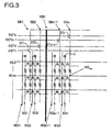
- Japanese Laid-Open Publication No. 5-198775 discloses a semiconductor memory device capable of regulating a difference in the load resistance of a bit line (hereinafter also simply referred to as bit line load resistance), which is caused depending on the position of a memory element. This device will be described below with reference to Figure 3.
- Figure 3 is an equivalent circuit diagram showing a memory array structure of a conventional semiconductor memory device.
- a memory array of the semiconductor memory device comprises: a plurality of virtual ground lines SG (SG1 to SGn, ...) arranged in parallel; a plurality of sub-bit lines SB (SB1 to SBn, ⁇ ) each provided between adjacent virtual ground lines SG; main-bit lines MB (MB1, ...) connected to respective groups of sub-bit lines, main groundlines MG (MG1 to MGn, ⁇ ) each connected to a plurality of virtual ground lines SG; a plurality of word select lines WL (WL0 to WLm, ⁇ ) provided along a direction intersecting the sub-bit line; a plurality of memory cells MC (MC 1,1 to MC m,n , ⁇ ) each provided between a virtual ground line SG and a sub-bit line SB; and switching elements ST (ST1 to STn, ⁇ ) provided between the main-bit line MB and the sub-bit line SB in the respective bit line groups.
- the memory cell MC comprises a MOS transistor, in which the virtual ground line SG is connected to the source terminal, the sub-bit line SB is connected to the drain terminal, and the word select line WL is connected to the gate terminal. Note that the main ground line MG overlaps the memory cell HC in Figure 3, but the main ground line MG is not connected to the memory cell MC.
- the gate terminals of the switching elements ST are connected to respective select signal lines SGT (SGT1 to SGTn, ⁇ ).
- the main-bit line MB and the main ground line MG are made of a metal conductor.
- the resistance of a conductor is negligible.
- the sub-bit line SB and the virtual ground line SG have an impurity diffusion region having a higher resistance than that of a metal conductor.
- the virtual ground line may also be referred to as a sub-bit line, and therefore, will be described below as a source-side sub-bit line SG.
- the total length of the impurity diffusion regions of the drain-side sub-bit line SB and the source-side sub-bit line SG, of a selected memory cell MC is set to be constant so as to reduce variations in driving current due to the dependency of the driving current on the total conductor resistance
- MC m,n a memory cell positioned on column n selected by the drain-side sub-bit line SBn and the source-side sub-bit line SGn and row m selected by an m-th word line WLm is referred to as MC m,n .
- the conductor resistance of the drain-side sub-bit line SBn of the memory cell MC m,n is m ⁇ r where r is a resistance per unit cell.
- the conductor resistance of the source-side sub-bit line SGn is (s-m) ⁇ r where s is a distance to a contact C of a sub-bit line (unit: bit).
- the total of the resistance of sub-bit lines (the sum of the drain-side and source-side conductor resistances: s ⁇ r) is constant.
- a memory cell MC m+k,n is located on the same column as that of the memory cell MC m,n (column n) and away by k on a row from the memory cell MC m,n .
- the conductor resistance of the drain-side sub-bit line SBm+k and the conductor resistance of the source-side sub-bit line SGm+k are (m+k) ⁇ r and (s-m-k) ⁇ r, respectively. Therefore, the sum of these sub-bit line resistances is s ⁇ r.
- the sum of sub-bit line resistances can be a constant value (s ⁇ r) in the driving current path of selected memory cells MC.
- the conventional technique has the following problems (1) and (2).
- a semiconductor memory device comprising: a plurality of memory elements; at least one bit line, wherein a memory operation is performed via at least a portion of the bit line with respect to at least one of the plurality of memory elements; and a load resistance regulating circuit for changing a resistance value to reduce or eliminate a difference in bit line load resistance depending on a position of the memory element.
- a semiconductor memory device further comprises: at least one word line, wherein the bit lines are arranged in parallel to one another, the word lines are arranged in parallel to one another, and the bit lines intersect the word lines, and each of the plurality of memory elements has two driving terminals connected to corresponding bit lines adjacently located, and a control terminal connected to a corresponding word line.
- each of the bit lines may has a first bit line made of an impurity diffusion region, a second bit linemade of a metal conductor connected to the first bit line, and a third bit line made of a metal conductor connected to an end of the second bit line via a bit line selecting element, and a voltage is supplied to one of the memory elements via the third bit line, the second bit line, and the first bit line.
- the second bit line comprises a plurality of branched lines connected to the third bit line.
- the load resistance regulating circuit is provided on a voltage supplying path between an end of the bit line and an output end of a voltage supplying circuit for supplying a predetermined voltage to the bit line.
- the load resistance regulating circuit changes a resistance value based on address information to reduce or eliminate a difference in a load resistance of a bit line in a row direction.
- the load resistance regulating circuit is a load resistance switching circuit having a plurality of resistance elements and a resistance element selecting means for selecting at least one of the plurality of resistance elements.
- the resistance element selectingmeans switches the resistance elements based on the address information of the memory element.
- the load resistance regulating circuit has a variable resistance element and a resistance value controlling means for controlling the variable resistance element to change the resistance value thereof.
- the resistance value controlling means changes the resistance value of the variable resistance element based on the address information of the memory element.
- a major portion of the resistance element has the same structure as that of the bit line and the major portion and the bit line are produced by the same production step.
- a major portion of the resistance element is produced using the same design protocol as that of at least a portion of the bit line.
- the load resistance regulating circuit controls a driving ability of the bit line selecting element to change a resistance value of the bit line selecting element to reduce or eliminate a difference in a load resistance of the bit line.
- the load resistance regulating circuit changes and outputs a control voltage of the bit line selecting element based on the address information of the memory element.
- the load resistance regulating circuit determines the resistance value so that a sum of load resistances between a driving terminal of the selected memory element and an output end of a voltage supplying circuit for supplying a voltage to the bit line is constant or within a predetermined range, irrespective of a position of the selected memory element,
- a first conductor length, from one driving terminal of the memory element to a voltage supplying circuit for supplying a voltage to the bit line, is equal to a second conductor length, from the other driving terminal of the memory element to the voltage supplying circuit, or a difference between the first and second conductor length is within a predetermined range.
- the semiconductor memory device has a contactless structure, in which two driving terminals of the memory element are made of an impurity diffusion region, a contact portion with respect to a metal conductor is not provided for each memory element, but a contact portion with respect to a metal conductor is provided for a plurality of memory elements.
- the memory element is a MOS transistor.
- the memory element utilizes a channel hot electron injection phenomenon to do memory operations, such as an information read operation, an information write operation, or an information erase operation.
- the present invention provides a semiconductor memory device comprising memory elements (memory cells (e.g., MOSFET, etc. )) having driving terminals (i.e., a source terminal and a drain terminal) connected to a first bit line (sub-bit line) made of, for example, an impurity diffusion region.
- the first bit line is connected to a voltage supplying circuit via a second bit line (sub-bit line) made of a metal conductor, a bit line selecting element, and a third bit line (main-bit line) made of a metal conductor.
- the semiconductor memory device is provided with a load resistance regulating circuit for regulating a difference in bit line load resistance depending on the position (address) of a memory cell to reduce or eliminate the difference.
- the load resistance regulating circuit for example, a load resistance switching circuit is provided between a memory cell and a voltage supplying circuit for supplying a voltage to a bit line.
- the load resistance switching circuit comprises a plurality of load resistance elements and a load resistance element selecting means (e.g., a multiplexer, etc.), for selecting a load resistance element based on information about the address position of the selected memory cell so that a different load resistance is provided depending on the position (address) of a memory cell on a bit line.
- a load resistance element selecting means e.g., a multiplexer, etc.
- a major portion of the load resistance element of the load resistance switching circuit preferably has the same structure as that of at least a portion of a bit line, and is preferably produced by the same production step.
- a major portion of the load resistance element of the load resistance switching circuit is preferably produced by the same design protocol as that of at least a portion of a bit line.
- the load resistance regulating circuit regulates (variable control) the driving ability of the bit line selecting element made of a transistor or the like by controlling a gate voltage, so that a difference in bit line load resistance depending on the position (address) of a memory cell can be reduced or eliminated.
- the load resistance of the source-side bit line is substantially equal to the load resistance of the drain-side bit line.
- the load resistance of the drain-side bit line and the load resistance of the source-side bit line of a memory cell viewed from a voltage supplying circuit are equal to each other, so that the bit line load resistance independent of the row address of the selected memory cell can be provided. Therefore, as is different from conventional techniques, (1) a driving current does not vary due to a substrate bias effect between the source terminal of a selected memory cell and a voltage supplying circuit; and (2) a load resistance does not vary on a main-bit line irrespective of the position of a sub-bit line. Therefore, a voltage drop (potential difference), between the source terminal or the drain terminal of a selected memory cell and the voltage supplying circuit, due to a driving current and a bit line load resistance becomes equal to each other. As a result, a drain voltage and a source voltage can be constant at an arbitrary address within a chip during a read operation, a write operation, and an erase operation.
- the present invention is particularly effective for non-volatile memory cells which utilize the channel hot electron injection phenomenon to do a write or read operation with respect to a memory element.
- the present invention is also effective for a contactless structure in which a contact with respect to a metal conductor is not provided for each memory cell.
- the load resistance of the drain-side bit line and the load resistance of the source-side bit line of a memory cell viewed from a voltage supplying circuit are equal to each other, so that the bit line load resistance independent of the row address of the selected memory cell can be provided. Therefore, a voltage drop (potential difference) between the source terminal or the drain terminal of a selected memory cell and the voltage supplying circuit due to a driving current and a bit line load resistance becomes equal to each other. Therefore, it is possible to reduce a variation in a drain voltage and a source voltage during a read operation and a write/erase operation caused by injection of hot carriers, thereby reducing a variation in performance due to the substrate bias effect. Thus, it is possible to accurately read information stored in a memory cell. Further, a variation in a threshold voltage during writing of information and after writing is reduced, resulting in an improvement of write precision.
- the invention described herein makes possible the advantages of providing a semiconductor memory device, in which the source-side and drain-side bit line load resistances of a memory cell transistor can be regulated so that a difference in bit line load resistance depending on the position of a memory element can be reduced or eliminated, and a variation in resistance value from a main-bit line to a sub-bit line depending on the position of a sub-bit line can be reduced or eliminated.
- a non-volatile semiconductor memory device which comprises memory cells made of a MOSFET, and in which the channel hot electron injection phenomenon is used to do a write or read operation with respect to each memory cell.
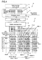
- Figure 1 is a diagram showing an equivalent circuit configuration of a memory array and its peripheral control circuit in a semiconductor memory device according to Embodiment 1 of the present invention.
- a semiconductor memory device 10 comprises a control circuit and a memory array 6.
- the control circuit comprises: a write/read bias supplying circuit 1 for supplying a driving voltage to a bit line; a load resistance switching circuit (load resistance regulating circuit 2) for regulating a bit line load resistance depending on the position of a memory cell MC; a write/read circuit 3 for controlling writing of data to a memory cell MC or reading of data from a memory cell MC; a column selecting circuit 4 for selecting the column of a memory cell MC; and a row selecting circuit 5 for selecting the row of a memory cell MC.
- the memory array 6 comprises a plurality of memory cells MC with respect to which write and read operations are performed by the control circuit.
- the memory array 6 comprises: a plurality of first bit lines (sub-bit lines) SBLA (SBLA1 to SBLAn, SBLAn+1, ⁇ ) arranged in parallel to one another; a plurality of second bit lines (sub-bit lines) SBLB (SBLB1 to SBLBn, SBLBn+1, ⁇ ) each provided on the left side of a corresponding sub-bit line SBLA; a plurality of third bit lines (main-bit lines) MBL ( ⁇ , MBLi, MBLi+1 , ⁇ ) each connected to a corresponding sub-bit line SBLB; a plurality of word select lines WL (WL0, ⁇ ,WLm, ⁇ ) arranged in parallel to one another in a direction intersecting the sub-bit lines SBLB (e.g., orthogonally) ; a plurality of memory cells MC ( ⁇ , MC m,1 to MC m,n , ⁇ ) each provided between adjacent sub-bit lines SBLA; a plurality of bit line selecting elements (
- MC m,n a memory cell positioned on column n selected by the sub-bit lines SBLAn and SBLBn and row m selected by a word line WLm.
- the memory cell MC m,n is made of a MOSFET (MOS transistor).
- the source terminal and the drain terminal thereof are connected to adjacent sub-bit lines SBLAn and SBLAn+1, which are formed on a semiconductor substrate by impurity diffusion.
- the gate terminal of a memory cell MC m,n is connected to the word select line WLm. Note that a sub-bit line SBLB is shown to overlap a memory cell MC m,n in Figure 1, but is not connected to the memory cell MC m,n .
- sub-bit lines SBLAn and SBLAn+1 are connected via respective contacts C provided on the opposite ends thereof to the sub-bit lines SBLBn and SBLBn+1, respectively, which are made of a metal conductor.
- the adjacent sub-bit lines SBLBn and SBLBn+1 are connected to one of the source terminal and the drain terminal of the sub-bit line select transistors STn and STn+1, respectively.
- the other of the source terminal and the drain terminal of each of the select transistors STn and STn+1 is connected to main-bit lines MBLi and MBLi+1. Because of this arrangement, the conductor length from the source terminal of each memory cell MC m,n to the write/ read bias supplying circuit 1 is substantially equal to the conductor length from the drain terminal of each memory cell MC m,n to the write/read bias supplying circuit 1.
- the column selecting circuit 4 is connected to the write/read circuit 3.
- the load resistance regulating circuit 2 (hereinafter referred to as a load resistance switching circuit 2) is provided between the write/read circuit 3 and the write/read bias supplying circuit 1 for supplying a bit line driving voltage.
- the load resistance switching circuit 2 has a plurality of load resistance element 2a arranged in parallel and having different resistance values, and a multiplexer circuit 2b for selecting at least one of the load resistance elements 2a.
- the multiplexer circuit 2b receives row address information on a bit line of a selected memory cell MC, and selects a load resistance element 2a based on the received row address information.
- Each load resistance element 2a has its major portion which has the same structure as that of at least a portion of a bit line, and is preferably produced in the same production step. In addition, each load resistance element 2a is preferably produced using the same design protocol as that of at least a portion of a bit line.
- the conductor resistance of the drain-side sub-bit line SBLAn+1 of a memory cell MC m,n is represented by: (1/(1/m+1/(s-m))) ⁇ r where r indicates the resistance value of a sub-bit line SBLA per unit cell, and s indicates a gap between each contact C connecting sub-bit lines SBLA and SBLB.
- the conductor resistance of the source-side sub-bit line SBLAn of a memory cell MC m,n is similarly calculated.
- the total load resistance of the drain-side bit line of a memory cell MC m,n is represented by: ⁇ (1/(1/m+1/(s-m))) ⁇ r+t+u ⁇ where t indicates the ON resistance value of a sub-bit line select transistor ST connected to the memory cell MC m,n , and u indicates a conductor resistance value from the column selecting circuit 4 to a main-bit line MBLi connected to the memory cell MC m,n .
- the total load resistance of the source-side bit line of a memory cell MC m,n is similarly calculated.
- the total load resistance of the bit line of a memory cell MC m,n on the bit lines can be represented by a function of m and u which are determined by the address of the memory cell MC m,n .
- a difference in bit line load resistance value (see expression (2)) depending on the position (address) of a memory cell is regulated to be reduced (within a predetermined range) or to be the same, in the following manner.
- the multiplexer circuit 2b selects a load resistance element 2a based on information about an address along a row direction on a bit line (row address information), and inserts a load resistance between the write/read circuit 3 and the write/read bias supplying circuit 1.
- the source-side or drain-side total load resistance of a memory cell MC m,n is represented by: ⁇ (1/(1/m+1/(s-m))) ⁇ r+t+u ⁇ +x where x indicates a load resistance value inserted between the write /read circuit 3 and the write/read bias supplying circuit 1.
- a bit line load resistance within a chip viewed from the write/read bias supplying circuit 1 can be regulated to be constant or within a predetermined range no matter which row address on a bit line is selected, i.e., no matter which memory cell MC m,n is selected.
- a memory cell MC m,n is connected to the bias supplying circuit 1 via a sub-bit line SBLA made of an impurity diffusion region, a sub-bit line SBLB made of a metal conductor, a bit line select transistor SGT, and a main-bit line MBL.
- the load resistance switching circuit 2 is provided between the memory array 6 and the bias supplying circuit 1, which regulates a difference in bit line load resistance depending on the position (address) of a memory cell MC m,n so that the difference is reduced (within a predetermined range) or the bit line load resistance is the same.
- the multiplexer 2b selects one of a plurality of load resistance elements 2a based on the row address information of a selected memory cell MC m,n so that the sum of the load resistances between the source terminal or the drain terminal of a memory cell MC m,n and the output terminal of the bias supplying circuit 1 is within a predetermined range.
- the multiplexer 2b selects one of a plurality of load resistance elements 2a based on the row address information of a selected memory cell MC m,n so that the sum of the load resistances between the source terminal or the drain terminal of a memory cell MC m,n and the output terminal of the bias supplying circuit 1 is within a predetermined range.
- the load resistance regulating circuit 2 is described as a load resistance switching circuit 2 having a plurality of load resistance elements 2a and a multiplexer 2b which is a resistance element selecting means for selecting at least one of the load resistance elements 2a.
- the present invention is not limited to this.
- the load resistance regulating circuit 2 may be, for example, configured to have a transistor or the like, which is a variable resistance element, and a resistance value controlling means for outputting a control voltage to the gate terminal of the transistor so that the resistance value of the transistor depends on the control voltage.
- the resistance value controlling means changes the conductive resistance value of the transistor (variable resistance element) depending on the address information (the position of a memory cell MC; e.g., row address information) of a memory element (memory cell MC).
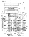
- Figure 2 is a diagram showing an equivalent circuit configuration of a memory array and a control circuit thereof in a semiconductor memory device according to Embodiment 2 of the present invention.
- a semiconductor memory device 20 has a load resistance regulating circuit 12 for regulating (variable control) the driving ability of a sub-bit line select transistor ST, as a load resistance regulating circuit for reducing or eliminating a difference in bit line load resistance, instead of the load resistance switching circuit 2 (load resistance switching circuit 2) of Figure 1.
- the load resistance regulating circuit 12 receives row address information of a memory cell MC m,n , and switches and outputs a plurality of voltages based on the row address information.
- the load resistance regulating circuit 12 switches output voltages based on information about an address position on a bit line (row address information) so as to reduce or eliminate a difference in bit line load resistance value depending on the position (address) of a memory cell according to the above-described expression (2). Specifically, a sub-bit line select signal is supplied to a sub-bit line selecting line SGT connected to the gate terminal of a sub-bit line select transistor ST. As a result, the driving ability of the sub-bit line select transistor ST is regulated (controlled), so that the ON resistance value t thereof is regulated (controlled).
- the source-side or drain-side total load resistance of a memory cell MC m,n is represented by: ⁇ (1/(1/m+1/(s-m))) ⁇ r+t'+u ⁇ where t' indicates the regulated ON resistance value of the bit line select transistor ST.
- a bit line load resistance within a chip viewed from the write/read bias supplying circuit 1 can be regulated to be constant or within a predetermined range no matter which row address on a bit line is selected, i.e., no matter which memory cell MC m,n is selected.
- Embodiments 1 and 2 two driving terminals (source terminal and drain terminal) of a memory cell MC (memory element) are made of an impurity diffusion region, a contact C with respect to a metal conductor is hot provided for each memory cell MC, but a contact C with respect to a metal conductor is provided for a plurality of memory cells MC.
- Embodiments 1 and 2 have a contactless structure.
- the above-described memory cell MC is a non-volatile memory element which utilizes the above-described channel hot electron injection phenomenon to do memory operations, such as an information read operation, an information write operation, or an information erase operation.
- the load resistance regulating circuit 12 sets a resistance value such that the sum of load resistances between a driving terminal of a selected memory element and the output terminal of a voltage supplying circuit for supplying a voltage to a bit line is constant or within a predetermined range, no matter where the selected memory element is located.
- the conductor length from one of the driving terminals of a memory element to a voltage supplying circuit, for supplying a voltage to a bit line may be equal to the conductor length from the other driving terminal of the memory element to the voltage supplying circuit, or the difference therebetween may be within a predetermined range.
- a sub-bit line has a resistance per unit conductor length higher than that of a main-bit line.
- the scale of a regulating circuit becomes excessively large.
- an auxiliary resistance element for an address for describing a relative position within a sub-bit line is provided to effectively regulate a bit line resistance value using a minimum circuit scale. In this case, it is not possible to cancel a difference in bit line resistance value due to a difference in the position of a sub-bit line on a main-bit line.
- the regulation range of the regulating circuit should be within the maximum difference in bit line resistance value due to a difference in the position of a memory element on a main-bit line.
- the maximum conductor length of a main-bit line has a resistance value of 500 ohm.
- a variation in the total resistance value of a selected bit line due to a difference in the address position of a selected word line is regulated to be within 500 ohm, assuming that the regulating circuit regulates a sub-bit line resistance, which is much greater than the resistance value of 500 ohm.
- a variation range in the total resistance value of a selected bit line in all word line addresses is preferably regulated to be equal to or smaller than the difference between the maximum resistance value in the total conductor length of a bit line and 50% of the maximum resistance value.
- non-volatile semiconductor memory devices such as non-volatile semiconductor memory devices (e.g., EEPROM, EPROM, etc.) and the like
- source-side and drain-side bit line load resistances to reduce or eliminate a difference in bit line load resistance depending on the address of a memory cell, and also reduce or eliminate a variation in the resistance value of a main-bit line depending on the position of a sub-bit line.
Landscapes
- Read Only Memory (AREA)
- Semiconductor Memories (AREA)
Applications Claiming Priority (2)
| Application Number | Priority Date | Filing Date | Title |
|---|---|---|---|
| JP2003311865 | 2003-09-03 | ||
| JP2003311865A JP4278140B2 (ja) | 2003-09-03 | 2003-09-03 | 半導体記憶装置 |
Publications (2)
| Publication Number | Publication Date |
|---|---|
| EP1513161A2 true EP1513161A2 (de) | 2005-03-09 |
| EP1513161A3 EP1513161A3 (de) | 2006-11-22 |
Family
ID=34131849
Family Applications (1)
| Application Number | Title | Priority Date | Filing Date |
|---|---|---|---|
| EP04255263A Withdrawn EP1513161A3 (de) | 2003-09-03 | 2004-08-31 | Halbleiter- Speicheranordnung |
Country Status (6)
| Country | Link |
|---|---|
| US (1) | US7283391B2 (de) |
| EP (1) | EP1513161A3 (de) |
| JP (1) | JP4278140B2 (de) |
| KR (1) | KR100628349B1 (de) |
| CN (1) | CN1591692B (de) |
| TW (1) | TWI251835B (de) |
Families Citing this family (14)
| Publication number | Priority date | Publication date | Assignee | Title |
|---|---|---|---|---|
| KR101258983B1 (ko) * | 2006-09-19 | 2013-04-29 | 삼성전자주식회사 | 가변저항 소자를 이용한 반도체 메모리 장치 및 그 동작방법 |
| JP4504397B2 (ja) * | 2007-05-29 | 2010-07-14 | 株式会社東芝 | 半導体記憶装置 |
| WO2009001534A1 (ja) * | 2007-06-22 | 2008-12-31 | Panasonic Corporation | 抵抗変化型不揮発性記憶装置 |
| KR101019895B1 (ko) * | 2009-06-23 | 2011-03-04 | 주식회사 하이닉스반도체 | 반도체 메모리 어레이 및 이를 포함하는 반도체 메모리 소자 |
| KR101642819B1 (ko) * | 2009-08-31 | 2016-07-26 | 삼성전자주식회사 | 비휘발성 메모리 장치, 그것의 구동 방법, 그것을 포함하는 메모리 시스템 |
| US8456930B2 (en) | 2010-10-07 | 2013-06-04 | Hynix Semiconductor Inc. | Variable resistance memory device having equal resistances between signal paths regardless of location of memory cells within the memory array |
| JP2012089747A (ja) | 2010-10-21 | 2012-05-10 | Toshiba Corp | 不揮発性半導体記憶装置 |
| JP2013004143A (ja) | 2011-06-16 | 2013-01-07 | Toshiba Corp | 不揮発性半導体記憶装置 |
| US8976581B2 (en) * | 2013-03-13 | 2015-03-10 | Macronix International Co., Ltd. | Non-volatile memory capable of programming cells by hot carrier injection based on a threshold voltage of a control cell |
| KR20160107566A (ko) * | 2015-03-04 | 2016-09-19 | 에스케이하이닉스 주식회사 | 저항변화 메모리 장치 및 그 동작 방법 |
| KR20160131180A (ko) * | 2015-05-06 | 2016-11-16 | 에스케이하이닉스 주식회사 | 전자 장치 및 그 동작방법 |
| KR102313601B1 (ko) | 2017-03-24 | 2021-10-15 | 삼성전자주식회사 | 메모리 장치의 동작 방법 |
| CN110718257A (zh) * | 2018-07-11 | 2020-01-21 | 西安格易安创集成电路有限公司 | 一种电压偏置电路及方法 |
| CN111951874B (zh) * | 2019-05-14 | 2022-10-18 | 兆易创新科技集团股份有限公司 | 一种校验的方法和装置 |
Citations (5)
| Publication number | Priority date | Publication date | Assignee | Title |
|---|---|---|---|---|
| US5295092A (en) * | 1992-01-21 | 1994-03-15 | Sharp Kabushiki Kaisha | Semiconductor read only memory |
| US5557124A (en) * | 1994-03-11 | 1996-09-17 | Waferscale Integration, Inc. | Flash EEPROM and EPROM arrays with select transistors within the bit line pitch |
| EP0797214A2 (de) | 1996-03-22 | 1997-09-24 | Sharp Kabushiki Kaisha | Halbleiterspeicheranordnung |
| US6175519B1 (en) | 1999-07-22 | 2001-01-16 | Macronix International Co., Ltd. | Virtual ground EPROM structure |
| US6480438B1 (en) | 2001-06-12 | 2002-11-12 | Ovonyx, Inc. | Providing equal cell programming conditions across a large and high density array of phase-change memory cells |
Family Cites Families (16)
| Publication number | Priority date | Publication date | Assignee | Title |
|---|---|---|---|---|
| US5258635A (en) * | 1988-09-06 | 1993-11-02 | Kabushiki Kaisha Toshiba | MOS-type semiconductor integrated circuit device |
| JP3083547B2 (ja) * | 1990-07-12 | 2000-09-04 | 株式会社日立製作所 | 半導体集積回路装置 |
| JP2642520B2 (ja) * | 1991-02-01 | 1997-08-20 | シャープ株式会社 | 半導体読出し専用メモリ |
| JPH08153391A (ja) * | 1994-11-29 | 1996-06-11 | Fujitsu Ltd | ダイナミックram |
| JP3169788B2 (ja) * | 1995-02-17 | 2001-05-28 | 日本電気株式会社 | 半導体記憶装置 |
| JPH08263985A (ja) * | 1995-03-24 | 1996-10-11 | Nec Corp | 半導体記憶装置 |
| US5679591A (en) * | 1996-12-16 | 1997-10-21 | Taiwan Semiconductor Manufacturing Company, Ltd | Method of making raised-bitline contactless trenched flash memory cell |
| US5798966A (en) * | 1997-03-31 | 1998-08-25 | Intel Corporation | Flash memory VDS compensation techiques to reduce programming variability |
| JP3990485B2 (ja) * | 1997-12-26 | 2007-10-10 | 株式会社ルネサステクノロジ | 半導体不揮発性記憶装置 |
| US6831316B1 (en) * | 1999-06-17 | 2004-12-14 | Hitachi, Ltd. | Semiconductor memory device and method of manufacturing the same |
| JP4212760B2 (ja) * | 2000-06-02 | 2009-01-21 | 富士通マイクロエレクトロニクス株式会社 | 半導体記憶装置 |
| US6594176B2 (en) * | 2001-01-24 | 2003-07-15 | Infineon Technologies Ag | Current source and drain arrangement for magnetoresistive memories (MRAMs) |
| EP1450373B1 (de) * | 2003-02-21 | 2008-08-27 | STMicroelectronics S.r.l. | Phasenwechselspeicheranordnung |
| US6826080B2 (en) * | 2002-05-24 | 2004-11-30 | Nexflash Technologies, Inc. | Virtual ground nonvolatile semiconductor memory array architecture and integrated circuit structure therefor |
| JP2004158119A (ja) * | 2002-11-06 | 2004-06-03 | Sharp Corp | 不揮発性半導体記憶装置 |
| KR100506457B1 (ko) * | 2003-07-30 | 2005-08-05 | 주식회사 하이닉스반도체 | 불휘발성 강유전체 메모리 셀 어레이 블럭 및 그 메모리셀 어레이 블럭을 이용하는 불휘발성 강유전체 메모리 장치 |
-
2003
- 2003-09-03 JP JP2003311865A patent/JP4278140B2/ja not_active Expired - Fee Related
-
2004
- 2004-08-31 EP EP04255263A patent/EP1513161A3/de not_active Withdrawn
- 2004-09-02 TW TW093126537A patent/TWI251835B/zh not_active IP Right Cessation
- 2004-09-03 US US10/934,212 patent/US7283391B2/en not_active Expired - Lifetime
- 2004-09-03 CN CN2004100686633A patent/CN1591692B/zh not_active Expired - Lifetime
- 2004-09-03 KR KR1020040070422A patent/KR100628349B1/ko not_active Expired - Lifetime
Patent Citations (5)
| Publication number | Priority date | Publication date | Assignee | Title |
|---|---|---|---|---|
| US5295092A (en) * | 1992-01-21 | 1994-03-15 | Sharp Kabushiki Kaisha | Semiconductor read only memory |
| US5557124A (en) * | 1994-03-11 | 1996-09-17 | Waferscale Integration, Inc. | Flash EEPROM and EPROM arrays with select transistors within the bit line pitch |
| EP0797214A2 (de) | 1996-03-22 | 1997-09-24 | Sharp Kabushiki Kaisha | Halbleiterspeicheranordnung |
| US6175519B1 (en) | 1999-07-22 | 2001-01-16 | Macronix International Co., Ltd. | Virtual ground EPROM structure |
| US6480438B1 (en) | 2001-06-12 | 2002-11-12 | Ovonyx, Inc. | Providing equal cell programming conditions across a large and high density array of phase-change memory cells |
Also Published As
| Publication number | Publication date |
|---|---|
| US20050057993A1 (en) | 2005-03-17 |
| KR20050025076A (ko) | 2005-03-11 |
| EP1513161A3 (de) | 2006-11-22 |
| TW200527434A (en) | 2005-08-16 |
| US7283391B2 (en) | 2007-10-16 |
| JP2005078779A (ja) | 2005-03-24 |
| TWI251835B (en) | 2006-03-21 |
| KR100628349B1 (ko) | 2006-09-27 |
| JP4278140B2 (ja) | 2009-06-10 |
| CN1591692A (zh) | 2005-03-09 |
| CN1591692B (zh) | 2013-06-12 |
Similar Documents
| Publication | Publication Date | Title |
|---|---|---|
| US5644533A (en) | Flash memory system, and methods of constructing and utilizing same | |
| EP1420408B1 (de) | Nichtflüchtige Halbleiterspeicheranordnung | |
| US5109361A (en) | Electrically page erasable and programmable read only memory | |
| KR100489988B1 (ko) | 스케일러블 플래시 eeprom 메모리 셀과 어레이 | |
| KR100446402B1 (ko) | 불휘발성 반도체 기억 장치의 프로그램 방법 | |
| US7283391B2 (en) | Semiconductor memory device | |
| US5010520A (en) | Nonvolatile semiconductor memory device with stabilized data write characteristic | |
| EP1256959A2 (de) | Programmierverfahren für einen nicht-flüchtigen Halbleiterspeicher mit Twin-Speicherzellen | |
| US7352625B2 (en) | Semiconductor memory device and memory card | |
| US6697280B2 (en) | Semiconductor capacitance device, booster circuit and nonvolatile semiconductor storage device | |
| EP1123547B1 (de) | Verfahren zur spalten-vorspannungs-einstellung zur beseitigung von programmierstörungen in einem nichtflüchtigen speicher und speicher zur anwendung des verfahrens | |
| US6707695B2 (en) | Nonvolatile semiconductor memory device | |
| KR101314328B1 (ko) | 비휘발성 메모리 소자 및 그 동작 방법 | |
| JP2003037191A (ja) | 不揮発性半導体記憶装置 | |
| US6574148B2 (en) | Dual bit line driver for memory | |
| KR100295794B1 (ko) | 대용량및고속소거에적합한반도체메모리장치 | |
| US6654282B2 (en) | Nonvolatile semiconductor memory device | |
| WO1994010686A1 (en) | Flash memory system, and methods of constructing and utilizing same | |
| JP3640179B2 (ja) | 不揮発性半導体記憶装置 | |
| US7800948B2 (en) | Nonvolatile semiconductor memory device | |
| US5175704A (en) | Nonvolatile semiconductor memory device | |
| KR0165468B1 (ko) | 반도체 메모리소자 및 그 제조방법 및 그 구동방법 | |
| US6819593B2 (en) | Architecture to suppress bit-line leakage | |
| JP2008217914A (ja) | 不揮発性半導体記憶装置 | |
| JP2692631B2 (ja) | 半導体不揮発性記憶装置 |
Legal Events
| Date | Code | Title | Description |
|---|---|---|---|
| PUAI | Public reference made under article 153(3) epc to a published international application that has entered the european phase |
Free format text: ORIGINAL CODE: 0009012 |
|
| AK | Designated contracting states |
Kind code of ref document: A2 Designated state(s): AT BE BG CH CY CZ DE DK EE ES FI FR GB GR HU IE IT LI LU MC NL PL PT RO SE SI SK TR |
|
| AX | Request for extension of the european patent |
Extension state: AL HR LT LV MK |
|
| PUAL | Search report despatched |
Free format text: ORIGINAL CODE: 0009013 |
|
| AK | Designated contracting states |
Kind code of ref document: A3 Designated state(s): AT BE BG CH CY CZ DE DK EE ES FI FR GB GR HU IE IT LI LU MC NL PL PT RO SE SI SK TR |
|
| AX | Request for extension of the european patent |
Extension state: AL HR LT LV MK |
|
| 17P | Request for examination filed |
Effective date: 20070201 |
|
| AKX | Designation fees paid |
Designated state(s): DE FR GB IT |
|
| 17Q | First examination report despatched |
Effective date: 20071220 |
|
| GRAJ | Information related to disapproval of communication of intention to grant by the applicant or resumption of examination proceedings by the epo deleted |
Free format text: ORIGINAL CODE: EPIDOSDIGR1 |
|
| GRAP | Despatch of communication of intention to grant a patent |
Free format text: ORIGINAL CODE: EPIDOSNIGR1 |
|
| RAP1 | Party data changed (applicant data changed or rights of an application transferred) |
Owner name: INTELLECTUAL PROPERTIES I KFT. |
|
| RAP1 | Party data changed (applicant data changed or rights of an application transferred) |
Owner name: XENOGENIC DEVELOPMENT LIMITED LIABILITY COMPANY |
|
| GRAP | Despatch of communication of intention to grant a patent |
Free format text: ORIGINAL CODE: EPIDOSNIGR1 |
|
| INTG | Intention to grant announced |
Effective date: 20150922 |
|
| STAA | Information on the status of an ep patent application or granted ep patent |
Free format text: STATUS: THE APPLICATION IS DEEMED TO BE WITHDRAWN |
|
| 18D | Application deemed to be withdrawn |
Effective date: 20160203 |