EP1507888B1 - Plasmaangeregtes chemisches gasphasenabscheide-verfahren zum abscheiden von siliziumnitrid oder siliziumoxinitrid in einem mim-kondensator - Google Patents
Plasmaangeregtes chemisches gasphasenabscheide-verfahren zum abscheiden von siliziumnitrid oder siliziumoxinitrid in einem mim-kondensator Download PDFInfo
- Publication number
- EP1507888B1 EP1507888B1 EP03755893A EP03755893A EP1507888B1 EP 1507888 B1 EP1507888 B1 EP 1507888B1 EP 03755893 A EP03755893 A EP 03755893A EP 03755893 A EP03755893 A EP 03755893A EP 1507888 B1 EP1507888 B1 EP 1507888B1
- Authority
- EP
- European Patent Office
- Prior art keywords
- flow rate
- silane
- silicon
- layer
- plasma
- Prior art date
- Legal status (The legal status is an assumption and is not a legal conclusion. Google has not performed a legal analysis and makes no representation as to the accuracy of the status listed.)
- Expired - Lifetime
Links
Images


Classifications
-
- H—ELECTRICITY
- H10—SEMICONDUCTOR DEVICES; ELECTRIC SOLID-STATE DEVICES NOT OTHERWISE PROVIDED FOR
- H10P—GENERIC PROCESSES OR APPARATUS FOR THE MANUFACTURE OR TREATMENT OF DEVICES COVERED BY CLASS H10
- H10P14/00—Formation of materials, e.g. in the shape of layers or pillars
- H10P14/60—Formation of materials, e.g. in the shape of layers or pillars of insulating materials
- H10P14/69—Inorganic materials
- H10P14/694—Inorganic materials composed of nitrides
- H10P14/6943—Inorganic materials composed of nitrides containing silicon
- H10P14/69433—Inorganic materials composed of nitrides containing silicon the material being a silicon nitride not containing oxygen, e.g. SixNy or SixByNz
-
- C—CHEMISTRY; METALLURGY
- C23—COATING METALLIC MATERIAL; COATING MATERIAL WITH METALLIC MATERIAL; CHEMICAL SURFACE TREATMENT; DIFFUSION TREATMENT OF METALLIC MATERIAL; COATING BY VACUUM EVAPORATION, BY SPUTTERING, BY ION IMPLANTATION OR BY CHEMICAL VAPOUR DEPOSITION, IN GENERAL; INHIBITING CORROSION OF METALLIC MATERIAL OR INCRUSTATION IN GENERAL
- C23C—COATING METALLIC MATERIAL; COATING MATERIAL WITH METALLIC MATERIAL; SURFACE TREATMENT OF METALLIC MATERIAL BY DIFFUSION INTO THE SURFACE, BY CHEMICAL CONVERSION OR SUBSTITUTION; COATING BY VACUUM EVAPORATION, BY SPUTTERING, BY ION IMPLANTATION OR BY CHEMICAL VAPOUR DEPOSITION, IN GENERAL
- C23C16/00—Chemical coating by decomposition of gaseous compounds, without leaving reaction products of surface material in the coating, i.e. chemical vapour deposition [CVD] processes
- C23C16/22—Chemical coating by decomposition of gaseous compounds, without leaving reaction products of surface material in the coating, i.e. chemical vapour deposition [CVD] processes characterised by the deposition of inorganic material, other than metallic material
- C23C16/30—Deposition of compounds, mixtures or solid solutions, e.g. borides, carbides, nitrides
- C23C16/308—Oxynitrides
-
- C—CHEMISTRY; METALLURGY
- C23—COATING METALLIC MATERIAL; COATING MATERIAL WITH METALLIC MATERIAL; CHEMICAL SURFACE TREATMENT; DIFFUSION TREATMENT OF METALLIC MATERIAL; COATING BY VACUUM EVAPORATION, BY SPUTTERING, BY ION IMPLANTATION OR BY CHEMICAL VAPOUR DEPOSITION, IN GENERAL; INHIBITING CORROSION OF METALLIC MATERIAL OR INCRUSTATION IN GENERAL
- C23C—COATING METALLIC MATERIAL; COATING MATERIAL WITH METALLIC MATERIAL; SURFACE TREATMENT OF METALLIC MATERIAL BY DIFFUSION INTO THE SURFACE, BY CHEMICAL CONVERSION OR SUBSTITUTION; COATING BY VACUUM EVAPORATION, BY SPUTTERING, BY ION IMPLANTATION OR BY CHEMICAL VAPOUR DEPOSITION, IN GENERAL
- C23C16/00—Chemical coating by decomposition of gaseous compounds, without leaving reaction products of surface material in the coating, i.e. chemical vapour deposition [CVD] processes
- C23C16/22—Chemical coating by decomposition of gaseous compounds, without leaving reaction products of surface material in the coating, i.e. chemical vapour deposition [CVD] processes characterised by the deposition of inorganic material, other than metallic material
- C23C16/30—Deposition of compounds, mixtures or solid solutions, e.g. borides, carbides, nitrides
- C23C16/34—Nitrides
- C23C16/345—Silicon nitride
-
- H—ELECTRICITY
- H10—SEMICONDUCTOR DEVICES; ELECTRIC SOLID-STATE DEVICES NOT OTHERWISE PROVIDED FOR
- H10D—INORGANIC ELECTRIC SEMICONDUCTOR DEVICES
- H10D1/00—Resistors, capacitors or inductors
- H10D1/60—Capacitors
- H10D1/68—Capacitors having no potential barriers
-
- H—ELECTRICITY
- H10—SEMICONDUCTOR DEVICES; ELECTRIC SOLID-STATE DEVICES NOT OTHERWISE PROVIDED FOR
- H10P—GENERIC PROCESSES OR APPARATUS FOR THE MANUFACTURE OR TREATMENT OF DEVICES COVERED BY CLASS H10
- H10P14/00—Formation of materials, e.g. in the shape of layers or pillars
- H10P14/60—Formation of materials, e.g. in the shape of layers or pillars of insulating materials
- H10P14/63—Formation of materials, e.g. in the shape of layers or pillars of insulating materials characterised by the formation processes
- H10P14/6326—Deposition processes
- H10P14/6328—Deposition from the gas or vapour phase
- H10P14/6334—Deposition from the gas or vapour phase using decomposition or reaction of gaseous or vapour phase compounds, i.e. chemical vapour deposition
- H10P14/6336—Deposition from the gas or vapour phase using decomposition or reaction of gaseous or vapour phase compounds, i.e. chemical vapour deposition in the presence of a plasma [PECVD]
-
- H—ELECTRICITY
- H10—SEMICONDUCTOR DEVICES; ELECTRIC SOLID-STATE DEVICES NOT OTHERWISE PROVIDED FOR
- H10P—GENERIC PROCESSES OR APPARATUS FOR THE MANUFACTURE OR TREATMENT OF DEVICES COVERED BY CLASS H10
- H10P14/00—Formation of materials, e.g. in the shape of layers or pillars
- H10P14/60—Formation of materials, e.g. in the shape of layers or pillars of insulating materials
- H10P14/66—Formation of materials, e.g. in the shape of layers or pillars of insulating materials characterised by the type of materials
- H10P14/668—Formation of materials, e.g. in the shape of layers or pillars of insulating materials characterised by the type of materials the materials being characterised by the deposition precursor materials
- H10P14/6681—Formation of materials, e.g. in the shape of layers or pillars of insulating materials characterised by the type of materials the materials being characterised by the deposition precursor materials the precursor containing a compound comprising Si
- H10P14/6682—Formation of materials, e.g. in the shape of layers or pillars of insulating materials characterised by the type of materials the materials being characterised by the deposition precursor materials the precursor containing a compound comprising Si the compound being a silane, e.g. disilane, methylsilane or chlorosilane
-
- H—ELECTRICITY
- H10—SEMICONDUCTOR DEVICES; ELECTRIC SOLID-STATE DEVICES NOT OTHERWISE PROVIDED FOR
- H10P—GENERIC PROCESSES OR APPARATUS FOR THE MANUFACTURE OR TREATMENT OF DEVICES COVERED BY CLASS H10
- H10P14/00—Formation of materials, e.g. in the shape of layers or pillars
- H10P14/60—Formation of materials, e.g. in the shape of layers or pillars of insulating materials
- H10P14/69—Inorganic materials
- H10P14/692—Inorganic materials composed of oxides, glassy oxides or oxide-based glasses
- H10P14/6921—Inorganic materials composed of oxides, glassy oxides or oxide-based glasses containing silicon
- H10P14/6922—Inorganic materials composed of oxides, glassy oxides or oxide-based glasses containing silicon the material containing Si, O and at least one of H, N, C, F or other non-metal elements, e.g. SiOC, SiOC:H or SiONC
- H10P14/6927—Inorganic materials composed of oxides, glassy oxides or oxide-based glasses containing silicon the material containing Si, O and at least one of H, N, C, F or other non-metal elements, e.g. SiOC, SiOC:H or SiONC the material being a silicon oxynitride, e.g. SiON or SiON:H
Definitions
- the invention relates to a method for producing a MIM capacitor according to claim 1 or claim 8.
- Metal-insulator-metal (MIM) capacitors are typically constructed of a first metallic layer on a substrate, a dielectric layer disposed on the first metallic layer, and a second metallic layer disposed on the dielectric layer. The three layers of a MIM capacitor are applied to the substrate surface by semiconductor techniques.
- an MIM capacitor is interesting for a number of technical applications.
- an MIM capacitor can be used in a radio frequency (RF) circuit, in an analog integrated circuit, or in a high performance microprocessor (MPU).
- RF radio frequency
- MPU microprocessor
- an economically interesting application of an MIM capacitor is that it can be used as a storage capacitor in a DRAM (Dynamic Random Access Memory) memory.
- DRAM Dynamic Random Access Memory
- ⁇ is the relative dielectric constant of the medium introduced between the capacitor plates
- A is the area of a plate of the plate capacitor
- d is the plate spacing between the two plates of the capacitor.
- the area of the capacitor A can be chosen to be sufficiently large.
- the distance between the two plates i. the thickness d of the dielectric layer between the two metallic layers of the MIM capacitor, are chosen to be sufficiently small. If the layer thickness of a MIM capacitor falls below a dimension of about 50 nm, problems arise with respect to its electrical stability, for example electrical breakdowns can occur and electrical leakage currents can increase.
- the dielectric constant of the dielectric layer between the two metal layers of an MIM capacitor is as high as possible.
- silicon nitride layers used as dielectric layers of an MIM capacitor have the disadvantage that the breakdown electric field strength is relatively low (about 2MV / cm).
- a dielectric layer of an MIM capacitor is carried out according to the prior art, for example by means of thermal growth or according to the CVD method ("Chemical Vapor Deposition").
- the CVD process is a coating technology for depositing thin layers of gas phase on a solid substrate.
- the principle of the CVD method is that gaseous starting materials, so-called precursors, are passed over a substrate and chemically decomposed into their constituents, whereby a new layer grows on the substrate surface.
- the decomposition of the precursors is usually thermal, i. E. by heating the substrate.
- the actual deposition occurs involving a chemical reaction, for example, a volatile gaseous component reacts with another gas to form a solid material which is deposited on the substrate.
- the CVD method has the disadvantage that the process temperatures are relatively high.
- PECVD Plasma Enhanced Chemical Vapor Deposition
- PECVD plasma enhanced chemical vapor deposition
- the Gas phase reaction is triggered by thermal energy due to heating of the substrate, the PECVD method based on the transfer of a gas in the plasma state in the vicinity of the substrate surface.
- One of the reaction products is a solid substance which precipitates on the surface, whereby a new layer is formed.
- silicon nitride (SiN x ), silicon oxide (SiO x ) and silicon oxynitride (SiO y N z ) can be deposited using the PECVD method.
- a plasma is ignited between the substrate holder serving as an electrode and another electrode through a strong alternating electric field.
- the energy of the field breaks up the bonds of the gas molecules introduced into the PECVD reactor and decomposes the gas molecules.
- the resulting radicals can be moved by means of an optional second electric field in the direction of the substrate, where the highly reactive radicals precipitate and form the desired layer.
- the invention is based on the problem of providing a dielectric layer having a larger relative dielectric constant with substantially constant mechanical and electrical stability.
- silane, ammonia and nitrogen are used as precursors, the flow rate ratio of silane to ammonia is set between 1:20 and 6: 5, the flow rate ratio between silane and Nitrogen is adjusted between 1:40 and 3: 5 and the pressure in the process chamber is set between 260 Pa and 530 Pa.
- silane, nitrous oxide and nitrogen are used as precursors.
- the flow rate ratio of silane to dinitrogen monoxide is set between 1: 2 and 25: 4 and the flow rate ratio between silane and nitrogen is set between 1: 100 and 1:10.
- the flow rate ratios of the precursors of the PECVD method for producing a silicon nitride layer or a silicon oxynitride layer selected in accordance with the invention are clearly different from the prior art in that, in the case of depositing silicon nitride, the ratio of the flow rates of silane (SiH 4 ) to ammonia (NH 3 ) or in the deposition of silicon oxynitride, the ratio of the flow rates of silane to nitrous oxide (N 2 O) are increased.
- the layers of silicon nitride (SiN x ) or silicon oxynitride (SiO y N z ) produced according to the invention preferably have non-stoichiometric silicon components.
- such a layer is suitable for use as a dielectric layer of an MIM capacitor.
- a capacitor having the same capacitance C can be manufactured with a smaller area of the two metal cladding layers of the MIM capacitor.
- the silicon nitride or silicon oxynitride layer according to the invention as dielectric layer of an MIM capacitor to choose the thickness of the dielectric layer and thus the distance d between the two metallic cover layers at the same capacity larger, so that a higher mechanical and electrical stability of the MIM capacitor is achieved.
- a higher dielectric layer thickness in a MIM capacitor problems with electrical leakage currents between the metallic layers are avoided and electrical breakdowns at high electric fields are also avoided.
- the method according to the invention is based on the standard semiconductor technology PECVD, as can be carried out on commercially available PECVD reactors, for example the "Novellus Concept One". Therefore, it is possible to produce the silicon-rich silicon nitride or silicon oxynitride layers according to the invention with a moderate outlay.
- the generation of the plasma from the precursors silane, ammonia and nitrogen introduced into the process space preferably takes place by means of a high-frequency field with a power of between approximately 300W and 700W.
- a low frequency field having a power between about 300W and 700W may be applied to the substrate to accumulate plasma in an environmental region of the substrate.
- the flow rate of silane is adjusted to a value between 100 standard cubic centimeters per minute and 600 standard cubic centimeters per minute.
- the method sets the flow rate ratio of silane to ammonia between 1:10 and 3: 5, the flow rate ratio between silane and nitrogen between 1:20 and 3:20, the pressure in the process chamber between 360Pa and 430Pa, and the power of the radio frequency Field as well as the power of the low frequency field independently of each other to a value between about 400W and 600W.
- the method sets the flow rate ratio of silane to ammonia at about 3:10, the flow rate ratio between silane and nitrogen is set to about 3:16, the pressure in the process chamber is set to about 350Pa, and the High-frequency power and the low-frequency power can be set to about 500W each.
- the flow rate of silane may be adjusted to about 300 standard cubic centimeters per minute according to this refinement.
- the pressure in the process chamber is preferably set between 260 Pa and 530 Pa.
- a high frequency field with a power between 200W and 500W can be applied to generate the plasma.
- a low frequency field having a power of up to 300W for accumulating plasma may be applied in an environmental area of the substrate.
- the low frequency field is not necessarily required and may optionally be omitted.
- the flow rate of silane is preferably adjusted to between 100 and 500 standard cubic centimeters per minute.
- the flow rate ratio of silane to dinitrogen monoxide is set between 1: 1 and 25: 8
- the flow rate ratio between silane and nitrogen is set between 1:50 and 1:20
- the pressure in set the process chamber between 350Pa and 430Pa and set the power of the high frequency field to a value between 300W and 400W and the power of the low frequency field to a value of up to 150W.
- the low frequency field may be omitted.
- the flow rate of silane is set at about 130 standard cubic centimeters per minute.
- the substrate used is preferably a semiconductor substrate, for example a silicon substrate such as a silicon wafer or a silicon chip.
- a metal is used for the first and / or the second electrically conductive material.
- the layer arrangement produced according to the method is preferably used as an MIM capacitor.
- the risk may exist that due to variations in the process control and / or due to other undesirable effects, the electrically insulating property of a formed layer, for example a silicon oxide or silicon oxynitride layer , is not achieved in an ideal way.
- a layer may undesirably have some residual electrical conductivity.
- the methods described below are provided according to the invention with which the electrically insulating property of a layer, for example of a silicon oxide or silicon oxynitride layer produced according to the invention, can be improved.
- the deposition process is interrupted at least once and continued after a vorgebaren waiting time, so that the electrically insulating layer of n + 1 sub-layers is formed, where n is the number of interruptions.
- the plasma-assisted deposition process is interrupted once or several times and in each case continued after a waiting time.
- an approximately electrically insulating layer to be produced according to the invention for example a silicon oxide or silicon oxynitride layer
- the electrical insulation property of an approximately electrically insulating layer to be produced according to the invention is improved by possibly being deposited in a deposited state
- Layer containing electrically conductive regions, such as unsaturated silicon bonds in a silicon oxide layer are oxidized in an oxygen-containing plasma and thus saturated.
- a surface treatment in an oxygen-containing plasma for example an oxygen plasma and / or a nitrous oxide plasma
- PECVD reactor 100 described a preferred embodiment of the plasma-enhanced chemical vapor deposition method according to the invention for depositing silicon nitride on a substrate described.
- the in Fig.1 PECVD reactor 100 shown has a process chamber 101.
- a silicon wafer 103 is mounted on a holding device 102.
- an electrode 104 divided into a plurality of sections is arranged, which has three openings 105a, 105b, 105c.
- 105a through the first opening provided a first valve 106a is open, silane gas (SiH 4) are introduced from the first reservoir 107a in the process chamber the one hundred and first Further, it can be introduced into the process chamber 101 through the second opening 105b containing a second valve is opened 106b, ammonia gas (NH 3) into the process chamber.
- SiH 4 silane gas
- nitrogen gas may be introduced into the process chamber 101 from the third reservoir 107c through a third port 105c.
- the electrode 104 is coupled to an RF voltage source 108 for generating a high frequency electric field in the process chamber.
- the holding device 102 with an LF voltage source 109 for generating a low-frequency voltage signal and applying it to the holding device 102 and to the wafer 103 coupled.
- the PECVD reactor 100 has a gas outlet 110, from which gas, if the fourth valve 111 is opened, can be removed from the process chamber 101.
- a pump 112 is shown, with the unneeded reaction products are pumped out through the gas outlet 110 from the process chamber 101 and with which a desired pressure in the process chamber 101 is set.
- such a high-frequency voltage is applied to the electrode 104 by means of the HF voltage source 108 that a strong alternating electric field is produced by means of the electrode 104 in the process chamber 101.
- silane is introduced into the process chamber 101 at a suitable flow rate, which can be set, for example, by adjusting the first valve 106 a.
- ammonia gas of a suitable flow rate is introduced into the process chamber 101 from the second reservoir 107, the flow rate being adjustable, for example, by means of the second valve 106b.
- nitrogen gas of an appropriate flow rate which is adjusted by adjusting the third valve 106c, is introduced into the process chamber 101.
- the gas molecules introduced are brought into the plasma state by means of the high-frequency electric field.
- the gas molecules are converted into radicals, for example, chemically highly reactive silicon radicals are generated from silane.
- a plasma 113 is formed.
- a low-frequency electrical voltage is applied to the wafer 103 via the holding device 102 by means of the LF voltage source 109. This low-frequency voltage ensures that the wafer 103 is negatively biased against the positively charged plasma 113. Due to electrical forces, the radicals of the plasma 113 diffuse to the surface of the silicon wafer 103 and are adsorbed there.
- the radicals chemically react to form a silicon nitride layer 114 on the surface of the wafer 103.
- the reaction equation of this chemical reaction on the surface of the silicon wafer 103 has the following shape: SiH 4 + NH 3 + N 2 ⁇ SiN x + (2)
- silane, ammonia and nitrogen are used as precursors.
- the flow rate of silane is set to 300 standard cubic centimeters per minute
- the flow rate of ammonia is set to 1000 standard cubic centimeters per minute
- the flow rate of nitrogen is set to 1600 standard cubic centimeters per minute
- the pressure can be adjusted by adjusting the valve 111 and the operating parameters of the pump 112.
- the flow rate ratio of silane to ammonia is set to about 3:10, whereas the flow rate ratio between silane and nitrogen is set to about 3:16.
- the LF voltage source 109 is optional and only fulfills the function of accumulating the positively charged plasma in a surrounding area of the surface of the silicon wafer 103, whereby the occurrence of a chemical reaction on the surface of the silicon wafer 103 is favored.
- the LF voltage source 109 may also be omitted.
- 13.56 MHz is chosen as the frequency of the RF voltage source
- 100 kHz is chosen as the frequency for the LF voltage source according to the described embodiment.
- the "Novellus Concept One" system from Novellus TM is selected.
- the PECVD reactor 100 may also be used to carry out the plasma enhanced chemical vapor deposition method of the invention for depositing silicon oxynitride on a substrate.
- the inventive method before performing the inventive method in the first reservoir 107a of silane gas in the second reservoir 107b nitrous oxide (N 2 O) and in the third reservoir 107c nitrogen (N 2) filled.
- N 2 O nitrous oxide
- the flow rate of silane is set to 130 sccm
- the flow rate of dinitrogen monoxide is set to 120 sccm
- the flow rate of nitrogen is set to 8000 sccm
- the pressure in the process chamber 101 is set to approximately 350 Pa
- the high-frequency power of the rf Voltage source 108 is set at approximately 300W
- the LF voltage source 109 is turned off, ie not used.
- a basic idea of the invention can be clearly seen in the fact that a silicon nitride layer or a silicon oxynitride layer is provided, in which the proportion of silicon is increased by using the PECVD method and by means of a skillful process control, whereby due to the high relative dielectric constant of silicon, the relative dielectric constant of the resulting silicon nitride or silicon oxynitride layer is increased.
- the process gases silane, nitrogen as well as ammonia or dinitrogen monoxide
- a stoichiometrically exact adjustment of the silicon portion of the resulting silicon nitride or silicon oxynitride layers is made possible.
- a basic idea of the invention can also be seen in the fact that in the production of a silicon nitride layer using the PECVD process according to the invention, the flow rate of ammonia is reduced or for producing a Siliziumoxinitrid layer, the flow rate of nitrous oxide is reduced, so that a desired , specifiable stoichiometry is obtained with an increased high proportion of silicon in the resulting silicon nitride or silicon oxynitride layers.
- Fig.2 2 there is shown a diagram 200 showing a Fourier Transform Infrared Spectroscopy (FTIR) spectrum of silicon nitride films made in accordance with the present invention.
- FTIR Fourier Transform Infrared Spectroscopy
- the abscissa 201 shows the wavenumber k (in cm -1 ) of the infrared radiation radiated onto the silicon nitride layer produced according to the invention.
- the intensity of the absorbed infrared radiation (in arbitrary units) is plotted.
- Each peak in an FTIR spectrum is assigned a characteristic material or a characteristic chemical bond.
- the three curves 203, 204, 205 shown have peaks that are characteristic of NH bonds, Si-H bonds, and Si-N bonds, respectively. Therefore, the intensity of the respective peaks is a measure of the stoichiometric proportion of the corresponding element or the corresponding chemical bond in the investigated silicon nitride layer.
- a first curve 203 shows an FTIR spectrum as obtained by performing the plasma enhanced chemical vapor deposition method of the invention for depositing silicon nitride using an ammonia flow rate of 1500 standard cubic centimeters per minute.
- a second curve 204 corresponds to an ammonia flow rate of 2000 standard cubic centimeters per minute and a third curve 205 shows the FTIR spectrum at an ammonia flow rate of 4000 standard cubic centimeters per minute. It can be seen from the peak marked in the diagram 200 labeled "Si-H" that the lower the ammonia flow rate, the higher the proportion of silicon-hydrogen bonds in the resulting silicon nitride layer.
- a reduction in the ammonia flow rate leads to an increase in the silicon content in the resulting silicon nitride layer. Therefore, by reducing the ammonia flow rate when performing the PECVD method, the silicon content in the resulting silicon nitride layer can be increased and thereby the relative dielectric constant of the resulting layer can be increased.
- Fig. 3 is a diagram 300 showing the FTIR spectrum of silicon oxynitride layers made according to the present invention. Again, along the abscissa 301, the wavenumber k (in cm -1 ) of the incident infrared radiation is shown. Along the ordinate 302 the infrared absorption I (in arbitrary units) is plotted.
- the graph 300 shows a first curve 303 and a second curve 304.
- the first curve 303 shows the obtained FTIR spectrum of a silicon oxynitride layer produced according to the invention in the event that the nitrous oxide flow rate is set to 160 standard cubic centimeters per minute.
- the flow rate of nitrous oxide is set at 200 standard cubic centimeters per minute.
- a reduction in the dinitrogen monoxide flow rate leads to a relative shift in the Si-O / Si-N weighting the Si-N component.
- the proportion of nitrogen-ligated silicon increases as the dinitrogen monoxide flow rate is reduced.
- Stoichiometric silicon oxide occurs in the SiO 2 configuration such that the silicon dioxide has one-third silicon.
- the stoichiometric composition of silicon nitride is usually Si 3 N 4 , so that the silicon nitride component has 3/7 silicon.
- An increase in the nitrogen-ligated silicon component in the FTIR spectrum with a concomitant decrease in the oxygen-ligated silicon component therefore results in an increase in the silicon content in the silicon oxynitride layer, so that silicon-richer layers are obtained when the flow rate of nitrous oxide is reduced , Therefore, by reducing the flow rate of nitrous oxide (ie, by selecting the flow rate ratios according to the invention), the relative dielectric constant ⁇ of the resulting silicon oxynitride layer can be increased.
- FIG 400 A diagram 400 is shown based on RBS (Rayleigh Backscattering Spectroscopy) studies of silicon oxynitride layers made in accordance with the present invention.
- RBS Rayleigh Backscattering Spectroscopy
- the composition of a layer is determined by scattering high-energy ions on a solid due to the electrostatic potential of the atomic nuclei. From the spread spectrum, the quantitative composition of a tested layer can be determined.
- the components of the elements silicon (Si), oxygen (O) and nitrogen (N) determined from the RBS spectrum are plotted. Different dinitrogen monoxide flow rates but a constant silane flow rate were used to produce the associated silicon oxynitride layers.
- a first curve 403 shows the dependence of the silicon contribution in the silicon oxynitride layer for the different dinitrogen monoxide flow rates.
- a second curve 404 shows the dependence of the oxygen contribution in the prepared silicon oxynitride layers.
- a third curve 405 shows the contribution of the nitrogen component in the silicon oxynitride layers. How out Figure 4 As can be seen, there is a correlation between the silicon contribution in such prepared silicon oxynitride layer and the nitrous oxide flow rate used for the PECVD process. The lower the dinitrogen monoxide flow rate is chosen, the higher the relative proportion of silicon. Therefore, the relative dielectric constant of the resulting silicon oxynitride layer can be increased by decreasing the dinitrogen monoxide flow rate.
- a diagram 500 is shown which shows the dependence of the relative dielectric constant ⁇ (dimensionless) of a silicon nitride or silicon oxynitride layer produced according to the invention on the refractive index n (dimensionless) of the layer for light of a wavelength of 635 nm.
- the refractive index n is plotted.
- Values of the relative dielectric constant ⁇ of the silicon nitride or silicon oxynitride layers are plotted along the ordinate 502.
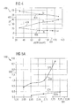
- Diagram 510 illustrates the dependence of a number of physical parameters of a silicon nitride layer produced on the ammonia flow rate dV / dt (in sccm) during the PECVD process according to the invention.
- abscissa 511 different flow rates of ammonia are plotted in standard cubic centimeters per minute.
- first ordinate 512 the refractive index n (dimensionless), the wet etching rate ds / dt (in nm per minute) and the compressive stress ⁇ of the silicon nitride layer (in 10 8 Pa) are plotted.
- the deposition rate dx / dt is plotted.
- a first curve 514 shows the dependence of the refractive index n of the silicon nitride layer produced according to the invention on the adjusted ammonia flow rate.
- FIG.5B there is a clear correlation between a reduction in ammonia flow rate dV / dt and an increase in refractive index n.
- Referring to FIG 5A corresponds to an increased Refractive index of a silicon nitride layer (see first curve 503) with an increase in the relative dielectric constant of the layer.
- a second curve 515 showing the dependence of the wet etch rate ds / dt (in nm per minute) on the ammonia flow rate dV / dt. Therefore, a reduced ammonia flow rate not only leads to an increase in the relative dielectric constant, but also to a marked reduction in the wet etch rate.
- a sufficiently low wet etching rate ensures that a defined etching back of a layer produced according to the invention is made possible. Since, with an increased dielectric constant, the wet etching rate of the silicon nitride layer produced according to the invention is reduced, further processing of such a layer is possible under defined conditions.
- a third curve 516 is shown, which shows the dependence of the compressive stress ⁇ (in 10 8 Pa) on the ammonia flow rate.
- graph 510 Also shown in graph 510 is a fourth graph 517 showing the dependence of the silicon nitride deposition rate on the ammonia flow rate. The lower the ammonia flow rate is chosen, the higher the deposition rate.
- the flow rate of nitrous oxide is plotted in the PECVD process according to the invention. Further, along a first ordinate 522, the refractive index n is plotted (dimensionless) and the wet etch rate ds / dt (in nm per minute) is plotted. Along a second ordinate 523, the deposition rate of silicon oxynitride, as obtained according to the method of the invention, is plotted.
- a first curve 524 in the graph 520 shows the dependence of the refractive index n on the dinitrogen monoxide flow rate. From the first curve 524 5C and from the second curve 504 5A For example, the correlation shows that a decrease in the dinitrogen monoxide flow rate leads to an increase in the relative dielectric constant ⁇ .
- a curve 525 off 5C shows the dependence of the wet etch rate ds / dt on the flow rate of nitrous oxide during the PECVD process.
- a reduction in the flow rate in this case of nitrous oxide leads to a reduction in the wet etching rate, so that further reduction of the dinitrogen monoxide flow rate enables further processing of the silicon oxynitride layer produced according to the invention under defined process conditions.
- a third plot 526 is shown showing the dependence of the silicon oxynitride removal rate on the nitrous oxide flow rate. Unlike in the case of the silicon nitride layer (compare curve 517 from diagram 510), in the case of silicon oxynitride, a reduction in the flow rate (in this case nitrous oxide) leads to a reduction in the deposition rate 526.
- the described physical parameters of the silicon nitride or silicon oxynitride layers produced according to the invention and the dependence of the physical parameters of these layers on the process conditions show that by means of a reduction of the flow rates of ammonia or nitrous oxide during a PECVD process, layers with an increased ⁇ and advantageous material properties are obtained.
- such layers have the required electrical, mechanical and optical properties to be suitable as dielectric layers of an MIM capacitor.
Landscapes
- Chemical & Material Sciences (AREA)
- Inorganic Chemistry (AREA)
- General Chemical & Material Sciences (AREA)
- Chemical Kinetics & Catalysis (AREA)
- Engineering & Computer Science (AREA)
- Materials Engineering (AREA)
- Mechanical Engineering (AREA)
- Metallurgy (AREA)
- Organic Chemistry (AREA)
- Chemical Vapour Deposition (AREA)
- Formation Of Insulating Films (AREA)
Applications Claiming Priority (3)
| Application Number | Priority Date | Filing Date | Title |
|---|---|---|---|
| DE10223954A DE10223954A1 (de) | 2002-05-29 | 2002-05-29 | Plasmaangeregtes chemisches Gasphasenabscheide-Verfahren zum Abscheiden von Siliziumnitrid oder Siliziumoxinitrid, Verfahren zum Herstellen einer Schicht-Anordnung und Schicht-Anordnung |
| DE10223954 | 2002-05-29 | ||
| PCT/DE2003/001552 WO2003102264A2 (de) | 2002-05-29 | 2003-05-14 | Verfahren zum abscheiden von siliziumnitrid oder siliziumoxinitrid sowie entsprechendes erzeugnis, |
Publications (2)
| Publication Number | Publication Date |
|---|---|
| EP1507888A2 EP1507888A2 (de) | 2005-02-23 |
| EP1507888B1 true EP1507888B1 (de) | 2010-12-22 |
Family
ID=29432440
Family Applications (1)
| Application Number | Title | Priority Date | Filing Date |
|---|---|---|---|
| EP03755893A Expired - Lifetime EP1507888B1 (de) | 2002-05-29 | 2003-05-14 | Plasmaangeregtes chemisches gasphasenabscheide-verfahren zum abscheiden von siliziumnitrid oder siliziumoxinitrid in einem mim-kondensator |
Country Status (6)
| Country | Link |
|---|---|
| US (1) | US7294553B2 (https=) |
| EP (1) | EP1507888B1 (https=) |
| JP (1) | JP4825418B2 (https=) |
| DE (2) | DE10223954A1 (https=) |
| TW (1) | TWI312543B (https=) |
| WO (1) | WO2003102264A2 (https=) |
Families Citing this family (24)
| Publication number | Priority date | Publication date | Assignee | Title |
|---|---|---|---|---|
| WO2005031850A2 (en) * | 2003-09-26 | 2005-04-07 | California Institute Of Technology | Detection and reduction of dielectric breakdown in semiconductor devices |
| DE102004003337A1 (de) * | 2004-01-22 | 2005-08-18 | Infineon Technologies Ag | Plasmaangeregtes chemisches Gasphasenabscheide-Verfahren, Silizium-Sauerstoff-Stickstoff-haltiges Material und Schicht-Anordnung |
| US7097779B2 (en) | 2004-07-06 | 2006-08-29 | Tokyo Electron Limited | Processing system and method for chemically treating a TERA layer |
| DE102004050391B4 (de) * | 2004-10-15 | 2007-02-08 | Infineon Technologies Ag | Verfahren zum Herstellen einer Schicht-Anordnung und Schicht-Anordnung |
| US7268038B2 (en) * | 2004-11-23 | 2007-09-11 | Newport Fab, Llc | Method for fabricating a MIM capacitor having increased capacitance density and related structure |
| JP5186776B2 (ja) | 2007-02-22 | 2013-04-24 | 富士通株式会社 | 半導体装置及びその製造方法 |
| US7606021B2 (en) * | 2007-02-26 | 2009-10-20 | United Microelectronics Corp. | Metal-insulator-metal capacitor and method for fabricating the same |
| US20090071371A1 (en) * | 2007-09-18 | 2009-03-19 | College Of William And Mary | Silicon Oxynitride Coating Compositions |
| US7678715B2 (en) * | 2007-12-21 | 2010-03-16 | Applied Materials, Inc. | Low wet etch rate silicon nitride film |
| US7943527B2 (en) * | 2008-05-30 | 2011-05-17 | The Board Of Trustees Of The University Of Illinois | Surface preparation for thin film growth by enhanced nucleation |
| KR101017763B1 (ko) * | 2008-10-16 | 2011-02-28 | 주식회사 동부하이텍 | Mim 커패시터 및 그 제조 방법 |
| US8563095B2 (en) * | 2010-03-15 | 2013-10-22 | Applied Materials, Inc. | Silicon nitride passivation layer for covering high aspect ratio features |
| JP5922352B2 (ja) * | 2011-08-11 | 2016-05-24 | Sppテクノロジーズ株式会社 | 窒化膜の製造装置及びその製造方法、並びにその製造プログラム |
| CN103094076B (zh) * | 2011-11-02 | 2015-12-16 | 无锡华润上华半导体有限公司 | 用于提高0.18μm工艺MIM电容性能的方法 |
| CN103060778B (zh) * | 2013-01-23 | 2015-03-11 | 深圳市劲拓自动化设备股份有限公司 | 平板式pecvd装置 |
| US9018108B2 (en) | 2013-01-25 | 2015-04-28 | Applied Materials, Inc. | Low shrinkage dielectric films |
| JP2015149404A (ja) * | 2014-02-06 | 2015-08-20 | 富士フイルム株式会社 | シリコンオキシナイトライド膜およびその製造方法、トランジスタ |
| US10693062B2 (en) * | 2015-12-08 | 2020-06-23 | Crossbar, Inc. | Regulating interface layer formation for two-terminal memory |
| GB201813467D0 (en) * | 2018-08-17 | 2018-10-03 | Spts Technologies Ltd | Method of depositing silicon nitride |
| US11710631B2 (en) * | 2020-10-23 | 2023-07-25 | Applied Materials, Inc. | Tensile nitride deposition systems and methods |
| WO2023017780A1 (ja) * | 2021-08-11 | 2023-02-16 | 株式会社村田製作所 | 弾性波装置 |
| KR102438504B1 (ko) * | 2021-11-24 | 2022-08-31 | 주식회사 아이에스티이 | SiCN 박막 형성 방법 |
| CN115955913A (zh) * | 2023-02-13 | 2023-04-11 | 广州粤芯半导体技术有限公司 | 电容结构及其制备方法、半导体结构 |
| CN119486379A (zh) * | 2023-08-04 | 2025-02-18 | 北京北方华创微电子装备有限公司 | 一种电流阻挡层的制备方法及led芯片 |
Family Cites Families (18)
| Publication number | Priority date | Publication date | Assignee | Title |
|---|---|---|---|---|
| US4618541A (en) * | 1984-12-21 | 1986-10-21 | Advanced Micro Devices, Inc. | Method of forming a silicon nitride film transparent to ultraviolet radiation and resulting article |
| US4786612A (en) * | 1986-02-03 | 1988-11-22 | Intel Corporation | Plasma enhanced chemical vapor deposited vertical silicon nitride resistor |
| GB2186116B (en) * | 1986-02-03 | 1989-11-22 | Intel Corp | Plasma enhanced chemical vapor deposited vertical resistor |
| US5164339A (en) * | 1988-09-30 | 1992-11-17 | Siemens-Bendix Automotive Electronics L.P. | Fabrication of oxynitride frontside microstructures |
| GB2231200A (en) * | 1989-04-28 | 1990-11-07 | Philips Electronic Associated | Mim devices, their method of fabrication and display devices incorporating such devices |
| US5284789A (en) * | 1990-04-25 | 1994-02-08 | Casio Computer Co., Ltd. | Method of forming silicon-based thin film and method of manufacturing thin film transistor using silicon-based thin film |
| GB9206086D0 (en) * | 1992-03-20 | 1992-05-06 | Philips Electronics Uk Ltd | Manufacturing electronic devices comprising,e.g.tfts and mims |
| US6083852A (en) * | 1997-05-07 | 2000-07-04 | Applied Materials, Inc. | Method for applying films using reduced deposition rates |
| US6316820B1 (en) * | 1997-07-25 | 2001-11-13 | Hughes Electronics Corporation | Passivation layer and process for semiconductor devices |
| US6287951B1 (en) * | 1998-12-07 | 2001-09-11 | Motorola Inc. | Process for forming a combination hardmask and antireflective layer |
| US6221794B1 (en) * | 1998-12-08 | 2001-04-24 | Advanced Micro Devices, Inc. | Method of reducing incidence of stress-induced voiding in semiconductor interconnect lines |
| JP3575307B2 (ja) | 1998-12-28 | 2004-10-13 | トヨタ自動車株式会社 | 排ガス浄化用触媒及びその製造方法 |
| US6309932B1 (en) * | 1999-01-14 | 2001-10-30 | Agere Systems Guardian Corp | Process for forming a plasma nitride film suitable for gate dielectric application in sub-0.25 μm technologies |
| US6171978B1 (en) | 1999-05-27 | 2001-01-09 | Taiwan Semiconductor Manufacturing Company | Method of manufacturing capacitor dielectric |
| US6242367B1 (en) * | 1999-07-13 | 2001-06-05 | Advanced Micro Devices, Inc. | Method of forming silicon nitride films |
| TW478158B (en) * | 1999-12-13 | 2002-03-01 | Lg Philips Lcd Co Ltd | Silicon oxide film forming method and manufacturing method of thin-film transistor |
| US6372668B2 (en) * | 2000-01-18 | 2002-04-16 | Advanced Micro Devices, Inc. | Method of forming silicon oxynitride films |
| US6383874B1 (en) * | 2001-03-07 | 2002-05-07 | Advanced Micro Devices, Inc. | In-situ stack for high volume production of isolation regions |
-
2002
- 2002-05-29 DE DE10223954A patent/DE10223954A1/de not_active Withdrawn
-
2003
- 2003-05-14 JP JP2004510496A patent/JP4825418B2/ja not_active Expired - Fee Related
- 2003-05-14 WO PCT/DE2003/001552 patent/WO2003102264A2/de not_active Ceased
- 2003-05-14 US US10/515,611 patent/US7294553B2/en not_active Expired - Fee Related
- 2003-05-14 DE DE50313348T patent/DE50313348D1/de not_active Expired - Lifetime
- 2003-05-14 EP EP03755893A patent/EP1507888B1/de not_active Expired - Lifetime
- 2003-05-21 TW TW092113777A patent/TWI312543B/zh not_active IP Right Cessation
Also Published As
| Publication number | Publication date |
|---|---|
| TWI312543B (en) | 2009-07-21 |
| DE50313348D1 (de) | 2011-02-03 |
| JP4825418B2 (ja) | 2011-11-30 |
| WO2003102264A2 (de) | 2003-12-11 |
| JP2005530924A (ja) | 2005-10-13 |
| US7294553B2 (en) | 2007-11-13 |
| EP1507888A2 (de) | 2005-02-23 |
| US20060084236A1 (en) | 2006-04-20 |
| TW200403762A (en) | 2004-03-01 |
| DE10223954A1 (de) | 2003-12-11 |
| WO2003102264A3 (de) | 2004-04-08 |
Similar Documents
| Publication | Publication Date | Title |
|---|---|---|
| EP1507888B1 (de) | Plasmaangeregtes chemisches gasphasenabscheide-verfahren zum abscheiden von siliziumnitrid oder siliziumoxinitrid in einem mim-kondensator | |
| EP1678746B1 (de) | Verfahren zum Ausbilden eines Dielektrikums auf einer kupferhaltigen Metallisierung | |
| DE69205241T2 (de) | Plasmaunterstützte Gasphasenabscheidung von Silizium mit gepulster Gas-Einspeisung. | |
| DE69229809T2 (de) | Verfahren zur photochemischen Materialbehandlung unter Verwendung von einer zylindrischen Blitz-Lampe als Lichtquelle | |
| DE102019128268B4 (de) | Verfahren zum reduzieren von durchschlagausfällen in einem mim-kondensator | |
| DE69226814T2 (de) | CVD-Methode zur Bildung eines Siliziumoxydfilms | |
| DE4430120B4 (de) | Verfahren zur Erzeugung eines Dielektrikums | |
| DE10123858B4 (de) | Atomschicht-Abscheidungsverfahren zur Bildung einer Siliciumnitrid-haltigen Dünnschicht | |
| DE69010308T2 (de) | Verfahren zur Abscheidung von Siliziumdioxid hoher Qualität mittels durch Plasma aktivierter Abscheidung aus der Gasphase. | |
| DE69819030T2 (de) | Doppelfrequenz cvd verfahren und vorrichtung | |
| DE102008036766B4 (de) | Vorrichtung und Verfahren zum Erzeugen dielektrischer Schichten im Mikrowellenplasma | |
| DE3856483T2 (de) | Verfahren zur Herstellung von Dünnschichten | |
| DE60114304T2 (de) | Hexagonal- Bornitrid-Film mit niedriger dielektrischer Konstante ,Film mit dielektrischer Beschichtung und Verfahren zu seiner Herstellung und Plasma-CVD-Apparat | |
| DE69227086T2 (de) | Verfahren zur Herstellung einer dielektrischen BPSG-Zwischenschicht einer Halbleitervorrichtung | |
| DE3876303T2 (de) | Verfahren zur herstellung eines duennschichttransistors. | |
| DE1564963C3 (de) | Verfahren zum Herstellen eines stabilisierten Halbleiterbauelements | |
| DE4104762A1 (de) | Verfahren und vorrichtung zur bearbeitung einer oberflaeche | |
| DE69521786T2 (de) | Verfahren und Vorrichtung zur plasma-unterstützten zeilenweisen Dampfabscheidung | |
| DE3329065A1 (de) | Polymerschichten fuer elektronische schaltungen | |
| DE10032213B4 (de) | Verfahren zur Herstellung eines Kondensators für ein Halbleiterspeicherbauelement | |
| DE69420791T2 (de) | Dünnfilm-Halbleiteranordnung für Anzeigetafel mit aktiver Matrix und Verfahren zur Herstellung | |
| DE10240176A1 (de) | Ein dielektrischer Schichtstapel mit kleiner Dielektrizitätskonstante einschliesslich einer Ätzindikatorschicht zur Anwendung in der dualen Damaszenertechnik | |
| DE10250902A1 (de) | Verfahren zur Entfernung von Strukturelementen unter Verwendung eines verbesserten Abtragungsprozess bei der Herstellung eines Halbleiterelements | |
| DE10130936A1 (de) | Herstellungsverfahren für ein Halbleiterbauelement | |
| DE10240449B4 (de) | Verfahren zur Herstellung einer dielektrischen Schicht mit geringem Leckstrom, wobei eine erhöhte kapazitive Kopplung erzeugt wird |
Legal Events
| Date | Code | Title | Description |
|---|---|---|---|
| PUAI | Public reference made under article 153(3) epc to a published international application that has entered the european phase |
Free format text: ORIGINAL CODE: 0009012 |
|
| 17P | Request for examination filed |
Effective date: 20041129 |
|
| AK | Designated contracting states |
Kind code of ref document: A2 Designated state(s): AT BE BG CH CY CZ DE DK EE ES FI FR GB GR HU IE IT LI LU MC NL PT RO SE SI SK TR |
|
| RBV | Designated contracting states (corrected) |
Designated state(s): DE FR |
|
| 17Q | First examination report despatched |
Effective date: 20090908 |
|
| RAP1 | Party data changed (applicant data changed or rights of an application transferred) |
Owner name: INFINEON TECHNOLOGIES AG |
|
| GRAJ | Information related to disapproval of communication of intention to grant by the applicant or resumption of examination proceedings by the epo deleted |
Free format text: ORIGINAL CODE: EPIDOSDIGR1 |
|
| GRAP | Despatch of communication of intention to grant a patent |
Free format text: ORIGINAL CODE: EPIDOSNIGR1 |
|
| GRAP | Despatch of communication of intention to grant a patent |
Free format text: ORIGINAL CODE: EPIDOSNIGR1 |
|
| RTI1 | Title (correction) |
Free format text: PLASMA-ENHANCED CHEMICAL VAPOUR DEPOSITION METHOD FOR DEPOSITING SILICON NITRIDE OR SILICON OXYNITRID IN AN MIM-CAPACITOR |
|
| GRAS | Grant fee paid |
Free format text: ORIGINAL CODE: EPIDOSNIGR3 |
|
| GRAA | (expected) grant |
Free format text: ORIGINAL CODE: 0009210 |
|
| AK | Designated contracting states |
Kind code of ref document: B1 Designated state(s): DE FR |
|
| REF | Corresponds to: |
Ref document number: 50313348 Country of ref document: DE Date of ref document: 20110203 Kind code of ref document: P |
|
| REG | Reference to a national code |
Ref country code: DE Ref legal event code: R096 Ref document number: 50313348 Country of ref document: DE Effective date: 20110203 |
|
| PLBE | No opposition filed within time limit |
Free format text: ORIGINAL CODE: 0009261 |
|
| STAA | Information on the status of an ep patent application or granted ep patent |
Free format text: STATUS: NO OPPOSITION FILED WITHIN TIME LIMIT |
|
| 26N | No opposition filed |
Effective date: 20110923 |
|
| REG | Reference to a national code |
Ref country code: DE Ref legal event code: R097 Ref document number: 50313348 Country of ref document: DE Effective date: 20110923 |
|
| REG | Reference to a national code |
Ref country code: FR Ref legal event code: PLFP Year of fee payment: 14 |
|
| REG | Reference to a national code |
Ref country code: FR Ref legal event code: PLFP Year of fee payment: 15 |
|
| PGFP | Annual fee paid to national office [announced via postgrant information from national office to epo] |
Ref country code: FR Payment date: 20170523 Year of fee payment: 15 |
|
| PGFP | Annual fee paid to national office [announced via postgrant information from national office to epo] |
Ref country code: DE Payment date: 20170718 Year of fee payment: 15 |
|
| REG | Reference to a national code |
Ref country code: DE Ref legal event code: R119 Ref document number: 50313348 Country of ref document: DE |
|
| PG25 | Lapsed in a contracting state [announced via postgrant information from national office to epo] |
Ref country code: DE Free format text: LAPSE BECAUSE OF NON-PAYMENT OF DUE FEES Effective date: 20181201 Ref country code: FR Free format text: LAPSE BECAUSE OF NON-PAYMENT OF DUE FEES Effective date: 20180531 |