EP1469334A1 - Telescope a large bande - Google Patents
Telescope a large bande Download PDFInfo
- Publication number
- EP1469334A1 EP1469334A1 EP02790859A EP02790859A EP1469334A1 EP 1469334 A1 EP1469334 A1 EP 1469334A1 EP 02790859 A EP02790859 A EP 02790859A EP 02790859 A EP02790859 A EP 02790859A EP 1469334 A1 EP1469334 A1 EP 1469334A1
- Authority
- EP
- European Patent Office
- Prior art keywords
- light
- optical system
- surface part
- reflecting mirror
- system unit
- Prior art date
- Legal status (The legal status is an assumption and is not a legal conclusion. Google has not performed a legal analysis and makes no representation as to the accuracy of the status listed.)
- Granted
Links
Images


Classifications
-
- G—PHYSICS
- G02—OPTICS
- G02B—OPTICAL ELEMENTS, SYSTEMS OR APPARATUS
- G02B23/00—Telescopes, e.g. binoculars; Periscopes; Instruments for viewing the inside of hollow bodies; Viewfinders; Optical aiming or sighting devices
- G02B23/02—Telescopes, e.g. binoculars; Periscopes; Instruments for viewing the inside of hollow bodies; Viewfinders; Optical aiming or sighting devices involving prisms or mirrors
- G02B23/06—Telescopes, e.g. binoculars; Periscopes; Instruments for viewing the inside of hollow bodies; Viewfinders; Optical aiming or sighting devices involving prisms or mirrors having a focussing action, e.g. parabolic mirror
-
- B—PERFORMING OPERATIONS; TRANSPORTING
- B82—NANOTECHNOLOGY
- B82Y—SPECIFIC USES OR APPLICATIONS OF NANOSTRUCTURES; MEASUREMENT OR ANALYSIS OF NANOSTRUCTURES; MANUFACTURE OR TREATMENT OF NANOSTRUCTURES
- B82Y10/00—Nanotechnology for information processing, storage or transmission, e.g. quantum computing or single electron logic
-
- G—PHYSICS
- G02—OPTICS
- G02B—OPTICAL ELEMENTS, SYSTEMS OR APPARATUS
- G02B23/00—Telescopes, e.g. binoculars; Periscopes; Instruments for viewing the inside of hollow bodies; Viewfinders; Optical aiming or sighting devices
- G02B23/02—Telescopes, e.g. binoculars; Periscopes; Instruments for viewing the inside of hollow bodies; Viewfinders; Optical aiming or sighting devices involving prisms or mirrors
-
- G—PHYSICS
- G21—NUCLEAR PHYSICS; NUCLEAR ENGINEERING
- G21K—TECHNIQUES FOR HANDLING PARTICLES OR IONISING RADIATION NOT OTHERWISE PROVIDED FOR; IRRADIATION DEVICES; GAMMA RAY OR X-RAY MICROSCOPES
- G21K2201/00—Arrangements for handling radiation or particles
- G21K2201/06—Arrangements for handling radiation or particles using diffractive, refractive or reflecting elements
- G21K2201/061—Arrangements for handling radiation or particles using diffractive, refractive or reflecting elements characterised by a multilayer structure
Definitions
- the present invention relates to a broadband telescope, more particularly to a broadband telescope suitable for using for astronomic observation where light of a broad energy band is made incident.
- a normal incidence telescope for observing light of a predetermined energy which comprises a reflecting mirror, on the surface of which a multilayer film is formed and which reflects only light of a predetermined energy corresponding to the multilayer film at high reflectance, and a detector such as a semiconductor detector to which reflected light reflected by the reflecting mirror is condensed and which detects the light of a predetermined energy.
- a multilayer film of a conventional reflecting mirror has a narrow band in which only light of a predetermined energy is reflected at high reflectance, so that discovery of line spectrum in a celestial body, which fluctuates remarkably, is not expected.
- a telescope capable of observing the light in a broad energy band is desired.
- a telescope capable of performing observation outside aerosphere is desired.
- the multilayer film formed on the surface of the reflecting mirror exhibits high reflectance only to light of a predetermined energy, only the light of a predetermined energy reflected at high reflectance by the reflecting mirror can be observed, on which the multilayer film was formed, and there has been a problem that observation could not been performed with respect to light in a broad energy band which is the light in a region extending from visible light to x-ray, for example.
- the conventional normal incidence telescope single telescope can only observe the light of a predetermined energy corresponding to the multilayer film of the reflecting mirror, it is required to use a plurality of normal incidence telescopes each having the reflecting mirror on which the multilayer film reflecting light of different energy is formed in order to observe the light in a broad energy band by the conventional normal telescope.
- a new problem such as cost increase and securing of a wide space for arranging a plurality of normal incidence telescopes occurs.
- an oblique incidence optical system for obtaining high reflectance with respect to the region extending from visible light to x-ray, but the oblique incidence optical system has had various problems such as a narrow field of vision and a small effective area.
- the present invention has been made in view of the above-described problems involved in prior art, and its object is to provide a broadband telescope that utilizes the advantages of the normal incidence optical system and the oblique incidence optical system well to make it possible to observe light in a broad energy band.
- another object of the present invention is to provide a broadband telescope in which a composite telescope of the normal incidence optical system and the oblique incidence optical system reflects each light rays in a broad energy band extending from visible light to x-ray, for example, at high reflectance to achieve cost reduction and space saving and to make it possible to efficiently observe the light in a broad energy band.
- the present invention comprises: an oblique incidence optical system unit where light is made incident obliquely to a surface part that reflects incident light; a normal incidence optical system unit where light is made incident substantially vertically to a surface part that reflects incident light; and a detector to which reflected light reflected by the surface part of the oblique incidence optical system unit and reflected light reflected by the surface part of the normal incidence optical system unit are made incident and which spectrally detects the incident light.
- the advantages of the normal incidence optical system and the oblique incidence optical system are utilized well and the light in the broad energy band can be severally observed.
- the normal incidence optical system unit may be located inside comparing to the oblique incidence optical system unit, and the detector may be located on an optical axis. This realizes further space saving and the entire telescope can be smaller.
- the present invention comprises: an oblique incidence optical system unit, which has a first reflecting mirror reflecting incident light at a first surface part made up of paraboloid of revolution, and a second reflecting mirror reflecting light, which is reflected at the surface part of the first mirror, at a second surface part made up of hyperboloid of revolution; a normal incidence optical system unit, which has a third reflecting mirror that has a third surface part on which a multilayer film is formed, which continuously changes a periodic length along its depth direction to reflect each light of a predetermined energy in a region extending from vacuum ultraviolet ray to extreme ultraviolet ray and has high reflectance due to total reflection over a visible light region, and reflects the incident light at the third surface part, and a fourth reflecting mirror that has a fourth surface part on which a multilayer film is formed, which continuously changes the periodic length along its depth direction corresponding to the third surface part of the third reflecting mirror to reflect each light of a predetermined energy in the region extending from vacuum ultraviolet ray to extreme ultraviolet ray and has high reflectance due to total
- the oblique incidence optical system unit when light in a broad energy band are made incident to the first surface part of the first reflecting mirror of the oblique incidence optical system unit and the third surface part of the third reflecting mirror of the normal incidence optical system unit, the oblique incidence optical system unit reflects each light in a region extending from visible light to hard x-ray out of the light in a broad energy band at high reflectance, the normal incidence optical system unit reflects each light in a region extending from visible light to extreme ultraviolet ray out of the light in a broad energy band at high reflectance, and the detector spectrally detects the light reflected at the surface part of the oblique incidence optical system unit and the surface part of the normal incidence optical system unit, so that the light in a broad energy band, particularly the light in the region extending from visible light to x-ray can be observed.
- the confocal composite telescope of the normal incidence optical system and the oblique incidence optical system reflects each light in a broad energy band at high reflectance, cost reduction and space saving can be achieved and the light in a broad energy band can be efficiently observed simultaneously.
- the first reflecting mirror and the second reflecting mirror of the oblique incidence optical system unit constitute an aspherical reflecting mirror of an approximate cylindrical shape
- the normal incidence optical system unit is located within the inner diameter side of the aspherical reflecting mirror
- the detector is located on the optical axis. This realizes further space saving and the entire telescope can be smaller.
- the detector may be a superconducting tunnel junction device.
- each light in a broad energy band reflected by a single or a plurality of reflecting mirror(s) can be spectrally detected by a single detector.
- the telescope may comprise a filter that makes only light, which has higher energy than the reflected light reflected at the surface part of the normal incidence optical system unit out of the reflected light reflected at the surface part of the oblique incidence optical system unit, incident selectively to the detector.
- Fig. 1 shows the explanatory view of a conceptual constitution illustrating an example of the embodiments of the broadband telescope according to the present invention
- Fig. 2 shows the explanatory view of a schematic constitution illustrating an example of the embodiments of the broadband telescope according to the present invention.
- the broadband telescope 10 is constituted to comprise an oblique incidence optical system unit 12 where light is made incident to reflecting mirrors 30 obliquely, a normal incidence optical system unit 14 where light is made incident to a reflecting mirror 40 approximately vertically, and a superconducting tunnel junction device (STJ) 16 as a detector into which the reflected light from the oblique incidence optical system unit 12 and the reflected light from the normal incidence optical system unit 14 are condensed.
- STJ superconducting tunnel junction device
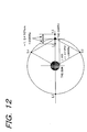
- the broadband telescope 10 comprises a cylindrical main unit 20 whose inside 20a is hollow. One end part of the main unit 20 is closed by an approximately circular bottom part 20b, and the other end part is open by an approximately circular opening 20c. Further, the telescope has a wall 20f, which divides the main unit 20 into a front section 20d and a rear section 20e, and a support 20g extended from the wall 20f.
- the central axis of the main unit 20 coincides with an axis passing through the center of the optical system of the oblique incidence optical system unit 12 that is an axis passing through the center of the optical system of the normal incidence optical system unit 12, that is, an axis O-O (refer to dashed line in Fig. 2) of the broadband telescope 10.
- the oblique incidence optical system unit 12 is constituted to comprise approximately cylindrical aspherical reflecting mirrors 12c of so-called Wolter type I and a filter 34 disposed on the wall 20f of the main unit 20 (refer to Fig. 3).
- the aspherical reflecting mirror 12c is constituted by a paraboloid 12a, which consists of a plurality of reflecting mirrors 30 disposed near the opening 20c of the front section 20d of the main unit, and a hyperboloid 12b that consists of a plurality of reflecting mirrors 32 near the wall 20f of the main unit 20.
- each of a plurality of the reflecting mirrors 30, which constitute the paraboloid 12a is in an approximately cylindrical body and includes a surface part 30a formed as the paraboloid of revolution.
- the entire body of each of a plurality of the reflecting mirrors 32, which constitute the hyperboloid 12b is in an approximately cylindrical body and includes a surface part 32a formed as the hyperboloid of revolution.
- Au (gold) or Pt (platinum) is coated on the surface part 30a of the reflecting mirrors 30 and the surface part 32a of the reflecting mirrors 32.
- the reflecting mirrors are disposed concentrically around the optical axis O-O in a multiple state such that each of a plurality of the reflecting mirrors 30 and each of a plurality of the reflecting mirrors 32 corresponds one to one, and the paraboloid 12a and the hyperboloid 12b are arranged in this order from the opening 20c of the main unit 20.
- one end part 30b of the reflecting mirrors 30 with the paraboloid 12 is located near the opening 20c of the main unit 20
- the other end part 30c of the reflecting mirrors 30 and one end part 32b of the reflecting mirrors 32 are adjacent to each other
- another end part 32c of the reflecting mirrors 32 is located closer to the wall 20f of the main unit 20.
- the filter 34 is in an approximate ring shape where an approximate circular hole 34a is formed at the central area, which is disposed in the wall 20f of the main unit 20 and located near the end part 32c of the reflecting mirrors 32.
- the filter 34 blocks light having energy same as that of extreme ultraviolet ray or less.
- the normal incidence optical system unit 14 is located within the inner diameter side of the approximately cylindrical aspherical reflecting mirrors 12c, which consist of the paraboloid 12a and the hyperboloid 12b of the oblique incidence optical system unit 12, and is constituted to comprise a reflecting mirror 40 supported by the support 20g in the front section 20d of the main unit 20, a reflecting mirror 42 supported by the front arm 20h extended from the support 20g, and a filter 44 supported by rear arm 20i extended from the support 20g (refer to Fig. 4).
- the normal incidence optical system unit 14 which consists of the reflecting mirror 40, the reflecting mirror 42 and the filter 44, constitutes a so-called Cassegrain-type telescope within the inner diameter side of the aspherical reflecting mirror 12c of the oblique incidence optical system unit 12.
- the surface part 40b of the reflecting mirror as the primary mirror and the surface part 42a of the reflecting mirror 42 as a secondary mirror face each other, the reflecting mirror 42 as the secondary mirror turns back an optical path, and focuses it on the rear surface part 40c of the reflecting mirror 40 as the primary mirror.
- the superconducting tunnel junction device 16 is arranged on the focused position in this embodiment.
- the reflecting mirror 40, the reflecting mirror 42 and the filter 44 are disposed such that the center of the reflecting mirror 40, the center of the reflecting mirror 42 and the center of the filter 44 coincide with the optical axis O-O of the broadband telescope 10.
- the entire reflecting mirror 40 is in a circular dish-shaped body 40a, and a hole part 40d that opens on the surface part 40b and the rear surface part 40c is formed on the central area. Further, the surface part 40b of the dish-shaped body 40a is formed as the paraboloid of revolution, which is concavely recessed centering around the hole part 40d (refer to Fig. 4 and Figs. 5(a), (b)).
- a first layer 40e-1 having a predetermined refractive index is formed and a second layer 40e-2, which has a refractive index different from the refractive index of the first layer 40e-1, is laminated on the first layer 40e-1. Furthermore, the first layer 40e-1 and the second layer 40e-2 laminated on the first layer 40e-1 make one set, a predetermined number n ('n' is a positive integer) of laminations are laminated to form a multilayer film 40e on the surface part 40b.
- the first layer 40e-1 is made from heavy element such as Ni (nickel) and Mo (molybdenum), for example, while the second layer 40e-2 is made from light element such as C (carbon) and Si (silicon), for example.
- the multilayer film 40e formed on the surface part 40b of the reflecting mirror 40 is a multilayer film having different periodic lengths d.
- the periodic lengths d of the multilayer film 40e are continuously changed in the depth direction (refer to Fig. 5(b)). More specifically, in the multilayer film 40e formed on the surface part 40b of the reflecting mirror 40, the periodic length d is designed to be shorter as a set of layers backs away from a surface 40ee and the periodic length d is designed to be longer as it approaches the surface 40ee along the depth direction of the multilayer film 40e.
- a periodic length d 1 farthermost away from the surface 40ee, a periodic length d 2 at the halfpoint in the depth direction, and a periodic length d 1 in the vicinity of the surface 40ee of the multilayer film 40e are in the relationship of the periodic length d 1 ⁇ the periodic length d 2 ⁇ the periodic length d 3 .
- the periodic lengths d of the multilayer film 40e formed on the surface part 40b of the reflecting mirror 40 are designed to be continuously changed in the depth direction of the multilayer film 40e so as to correspond to each light having a predetermined energy in the range extending from vacuum ultraviolet ray to extreme ultraviolet ray. Accordingly, energy of light reflected on the boundary surface between the first layer 40e-1 and the second layer 40e-2 utilizing Bragg reflection is different on different periodic lengths d (periodic length d 1 , d 2 , d 3 , for example) in the multilayer film 40e of the reflecting mirror 40.
- the "multilayer film where the periodic lengths d are continuously changed in the depth direction” is optionally referred to as a "supermirror”.
- the surface portion 42a of the reflecting mirror 42 has a convex surface and is constituted by the supermirror.
- the supermirror of the reflecting mirror 42 is designed corresponding to various conditions such as the type and the focal length of the supermirror that constitutes the surface part 40b as the concave surface of the reflecting mirror 40. Then, the surface part 42a of the reflecting mirror 42 reflects light reflected at the surface part 40b of the reflecting mirror 40 at high reflectance.
- the filter 44 is in an approximate disc-shaped body, which is supported by the rear support 20i of the main unit 20 and located in the vicinity of the hole part 40d of a rear surface part 40c side of the reflecting mirror 40.
- the filter 44 adjusts the quantity of light.
- the superconducting tunnel junction device 16 is a type of a Josephson device, which has a structure that a thin insulation film (aluminum oxide, for example) is sandwiched by superconducting metal thin films (niobium, aluminum, titanium, for example).
- the superconducting tunnel junction device 16 is a detector to which the reflected light from the oblique incidence optical system unit 12 and the reflected light from the normal incidence optical system unit 14 are condensed, as described above. More specifically, it operates at cryogenic temperature of approximately 0.3K, and when light is made incident to the superconducting tunnel junction device 16, energy of the incident light is absorbed by the superconducting metal thin films.
- the superconducting tunnel junction device 16 functions as a detector having high sensitivity and spectroscopic capability in a broadband extending form infrared ray to x-ray.
- Fig. 6(a) shows the reflectance on the surface of the superconducting tunnel junction device 16
- Fig. 6 (b) shows the transmittance of the superconducting tunnel junction device 16.
- photon absorptance of the superconducting tunnel junction device 16 is 95% or higher.
- the superconducting tunnel junction device 16 has very high photon absorptance in the region extending from extreme ultraviolet to soft x-ray, so that when the superconducting tunnel junction device 16 having behavior of producing signals by photon absorption as described above, spectral detection of light is realized in a region extending from visible light to hard x-ray.
- Fig. 7 shows the graph illustrating an example of energy resolution in a region extending from extreme ultraviolet ray to x-ray of the superconducting tunnel junction device 16
- Fig. 8 shows the graph illustrating an example of energy resolution in an x-ray region of the superconducting tunnel junction device 16
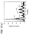
- Figs. 9(a), (b), (c) and (d) shows the graphs illustrating examples of energy resolution in a soft x-ray region of the superconducting tunnel junction device 16
- Figs. 9(e), (f), (g) and (h) shows the graphs illustrating examples of energy resolution in an extreme ultraviolet ray region of the superconducting tunnel junction device 16.
- a filter 50 is disposed in the prestage of the superconducting tunnel junction device 16.
- the filter 50 is in an approximate disc-shaped body and blocks infrared ray. For this reason, the filter 50 blocks infrared ray and infrared ray is not made incident to the superconducting tunnel junction device 16. Therefore, temperature rise of the superconducting tunnel junction device 16 is prevented, good operation environment is maintained, and more accurate detection result can be obtained.
- the electric current in proportion to the energy of the incident light is generated.
- Two circuit systems corresponding to signal levels are provided as the circuit system that takes out signals based on the electric current generated in this manner. Specifically, a circuit primarily for high energy such as x-ray and a circuit primarily for low energy such as visible light are disposed.
- the light reflected at the surface part 32a of the reflecting mirror 32 that is, light in the region extending from visible light to hard x-ray out of light in a broad energy band that has been made incident to the surface part 30a of the reflecting mirror 30 is made incident to the filter 34.
- the filter 34 blocks light having the same energy as that of extreme ultraviolet ray or less, light in the region extending from soft x-ray to hard x-ray transmits the filter 34, and condensed into the superconducting tunnel junction device 16 (refer to Fig. 10).
- each light having a predetermined energy out of light in a broad energy band which has been made incident to the surface part 40b of the reflecting mirror 40 as the primary mirror, transmits the multilayer film 40e on the surface part 40b of the reflecting mirror 40 in the depth direction according to an energy size, and is reflected at the boundary surface between the first layer 40e-1 and the second layer 40e-2, which has a corresponding periodic length d.
- the reflectance of the surface part 40b of the reflecting mirror 40 is reflectance where the reflectance of each boundary surface between the first layer 40e-1 and the second layer 40e-2, which has a predetermined periodic length d, of the multilayer film 40e and the reflectance of the surface part 40ee of the multilayer film 40e are superposed (refer to Fig. 10). Accordingly, the surface part 40b of the reflecting mirror 40 reflects each light in the region extending from visible light to extreme ultraviolet ray out of the incident light in a broad energy band at high reflectance.
- the light reflected by the supermirror that constitutes the surface part 40b of the reflecting mirror 40 is reflected by the supermirror that constitutes the surface part 42a of the reflecting mirror 42 as the secondary mirror.
- the supermirror that constitutes the surface part 42a of the reflecting mirror 42 is designed corresponding to the supermirror that constitutes the surface part 40b of the reflecting mirror 40 in order to reflect the light reflected at the surface part 40b of the reflecting mirror 40 at high reflectance. Therefore, each light in the region extending from visible light to extreme ultraviolet ray, which has been reflected by the surface part 40b of the reflecting mirror 40 at high reflectance, out of the light in a broad energy band, which has been made incident to the surface part 40b of the reflecting mirror 40 at high reflectance, is reflected at the surface part 42a of the reflecting mirror 42 at high reflectance.
- the light reflected at the surface part 42a of the reflecting mirror 42 that is, each light in the region extending from visible light to extreme ultraviolet ray out of the light in a broad energy band, which has been made incident to the surface part 40b of the reflecting mirror 40, goes through the hole part 40d of the reflecting mirror 40, transmits the filter 44, and is condensed into the superconducting tunnel junction device 16.
- the light in the region extending form soft x-ray to hard x-ray, which is the reflected light from the oblique incidence optical system unit 12, and the light in the region extending form visible light to extreme ultraviolet ray, which is the reflected light from the normal incidence optical system unit 14, out of the light in a broad energy band that has been made incident to the broadband telescope 10 are condensed and made incident into the superconducting tunnel junction device 16, the electric current in proportion to the energy of light that has been made incident as described above is generated.
- the signal is taken out in the circuit for high energy, and when the electric current is generated based on the light in the region extending form visible light to extreme ultraviolet ray, which is the reflected light from the normal incidence optical system unit 14, the signal is taken out in the circuit for low energy, and light in the region extending from visible light to hard x-ray is spectrally detected.
- the broadband telescope 10 comprises: the oblique incidence optical system unit 12 having the aspherical reflecting mirror 12c; the oblique incidence optical system unit 14 having the reflecting mirror 40 on which the supermirror corresponding to light in the region extending from visible light to extreme ultraviolet ray is formed; and the superconducting tunnel junction device 16 having high sensitivity and spectroscopic capability in a broadband extending from infrared ray to x-ray, the advantages of the normal incidence optical system and the oblique incidence optical system are utilized well.
- a single telescope that is the confocal composite telescope of the normal incidence optical system and the oblique incidence optical system reflects light in a broad energy band of the range extending from visible light to hard x-ray at high reflectance, and the superconducting tunnel junction device 16 spectrally detects the light.
- the light in a broad energy band, particularly the light in the range extending from visible light to x-ray can be observed by the broadband telescope 10 according to the present invention.
- the single telescope that is the confocal composite telescope of the normal incidence optical system and the oblique incidence optical system reflects light in a broad energy band of the range extending from visible light to hard x-ray at high reflectance, which eliminates the need of using a plurality of telescopes.
- cost reduction and space saving can be achieved and the light in a broad energy band can be efficiently observed simultaneously.
- the single telescope reflects light in a broad energy band of the range extending from visible light to hard x-ray at high reflectance, so that only one superconducting tunnel junction device 16 may be disposed to which the reflected light from the oblique incidence optical system unit 12 and the reflected light from the normal incidence optical system unit 14 are condensed, by which cost can be reduced and a single cooler for cooling the superconducting tunnel junction device 16 is sufficient.
- the broadband telescope 10 is mounted in performing astronomic observation.
- the superconducting tunnel junction device 16 is disposed at the rear surface side of the opening (that is, the end part 30b side of the reflecting mirror 30) of the aspherical reflecting mirror 12c of the oblique incidence optical system unit 12 and the rear surface side of the reflecting mirror 40 as the primary mirror of the normal incidence optical system unit 14, which facilitates the mounting of a cooling system such as the cooler for cooling the superconducting tunnel junction device 16.
- the broadband telescope 10 according to the present invention can be constituted so as to dispose the normal incidence optical system unit in an approximate columnar-shaped dead space formed in an inner diameter side of the aspherical reflecting mirror in the oblique incidence telescope so-called Wolter type I. For this reason, size reduction of the entire broadband telescope is easy, and the design know-how, etc. of the oblique incidence telescope can be utilized in such occasion.
- the superconducting tunnel junction device 16 is the detector that can perform one photon spectral detection from infrared ray to x-ray, it can separately identify the photon even if the observation scope of the oblique incidence optical system unit 12 and the normal incidence optical system unit 14 is different from each other.
- the present invention Since the present invention is constituted as described above, it exerts superior effect that the advantages of the normal incidence optical system and the oblique incidence optical system are utilized well and light in a broad energy band, which is light in the region extending from visible light to x-ray, for example, can be observed.
- the present invention since the present invention is constituted as described above, it exerts superior effect that a composite telescope of the normal incidence optical system and the oblique incidence optical system reflects the light in a broad energy band that is the region extending from visible light to x-ray, for example, at high reflectance, by which cost reduction and space saving can be achieved and the light in a broad energy band can be observed efficiently.
Applications Claiming Priority (3)
| Application Number | Priority Date | Filing Date | Title |
|---|---|---|---|
| JP2001397998 | 2001-12-27 | ||
| JP2001397998A JP4142289B2 (ja) | 2001-12-27 | 2001-12-27 | 広帯域望遠鏡 |
| PCT/JP2002/013484 WO2003056377A1 (fr) | 2001-12-27 | 2002-12-25 | Telescope a large bande |
Publications (3)
| Publication Number | Publication Date |
|---|---|
| EP1469334A1 true EP1469334A1 (fr) | 2004-10-20 |
| EP1469334A4 EP1469334A4 (fr) | 2007-06-13 |
| EP1469334B1 EP1469334B1 (fr) | 2011-06-15 |
Family
ID=19189269
Family Applications (1)
| Application Number | Title | Priority Date | Filing Date |
|---|---|---|---|
| EP02790859A Expired - Fee Related EP1469334B1 (fr) | 2001-12-27 | 2002-12-25 | Telescope a large bande |
Country Status (4)
| Country | Link |
|---|---|
| US (1) | US7450299B2 (fr) |
| EP (1) | EP1469334B1 (fr) |
| JP (1) | JP4142289B2 (fr) |
| WO (1) | WO2003056377A1 (fr) |
Cited By (1)
| Publication number | Priority date | Publication date | Assignee | Title |
|---|---|---|---|---|
| CN108572442A (zh) * | 2018-03-23 | 2018-09-25 | 同济大学 | 一种嵌套式分段型类Wolter-I型结构及其设计方法 |
Families Citing this family (9)
| Publication number | Priority date | Publication date | Assignee | Title |
|---|---|---|---|---|
| US7253939B2 (en) * | 2005-09-30 | 2007-08-07 | Intel Corporation | Superconductor-based modulator for extreme ultraviolet (EUV) |
| US7615385B2 (en) | 2006-09-20 | 2009-11-10 | Hypres, Inc | Double-masking technique for increasing fabrication yield in superconducting electronics |
| US20100328762A1 (en) * | 2009-04-27 | 2010-12-30 | Trex Enterprises Corp. | Radiation coating for silicon carbide components |
| FR2984584A1 (fr) * | 2011-12-20 | 2013-06-21 | Commissariat Energie Atomique | Dispositif de filtrage des rayons x |
| CN105093484B (zh) * | 2015-08-27 | 2017-12-22 | 北京控制工程研究所 | 一种多层嵌套圆锥面型x射线掠入射光学镜头 |
| JP6889897B2 (ja) * | 2016-06-10 | 2021-06-18 | 国立大学法人東海国立大学機構 | Frp製ミラー構造体の製造方法 |
| CN106569521B (zh) * | 2016-11-04 | 2018-12-21 | 北京控制工程研究所 | 一种用于x射线脉冲星导航敏感器的精密控温装置 |
| JP6921391B2 (ja) * | 2017-01-24 | 2021-08-18 | 国立研究開発法人宇宙航空研究開発機構 | 望遠鏡システム |
| WO2021162669A1 (fr) * | 2020-08-03 | 2021-08-19 | Roman Duplov | Dispositif de réduction des aberrations hors axe de systèmes optiques |
Citations (8)
| Publication number | Priority date | Publication date | Assignee | Title |
|---|---|---|---|---|
| GB729546A (en) * | 1951-07-31 | 1955-05-11 | Gustav Fries | Method and apparatus for optically projecting electron images |
| US3745347A (en) * | 1970-12-03 | 1973-07-10 | Philips Corp | Telescope including an imaging system for radiation in the visible range |
| JPS59222932A (ja) * | 1983-06-02 | 1984-12-14 | Sharp Corp | 半導体装置 |
| US4562583A (en) * | 1984-01-17 | 1985-12-31 | The United States Of America As Represented By The Administrator Of The National Aeronautics And Space Administration | Spectral slicing X-ray telescope with variable magnification |
| US4941163A (en) * | 1985-08-15 | 1990-07-10 | The United States Of America As Represented By The Administrator Of The National Aeronautics And Space Administration | Multispectral glancing incidence X-ray telescope |
| EP0670576A1 (fr) * | 1994-03-04 | 1995-09-06 | Osservatorio Astronomico Di Brera | Miroirs coaxiaux et confocaux à incidence rasante |
| JPH09113697A (ja) * | 1995-10-20 | 1997-05-02 | Nikon Corp | 多層膜反射鏡 |
| US5753935A (en) * | 1990-03-26 | 1998-05-19 | Nippon Steel Corporation | Superconductive tunnel junction array radiation detector |
Family Cites Families (13)
| Publication number | Priority date | Publication date | Assignee | Title |
|---|---|---|---|---|
| JPH0575169A (ja) | 1991-09-11 | 1993-03-26 | Hitachi Ltd | 光超伝導素子 |
| FR2711251B1 (fr) | 1993-10-15 | 1996-01-26 | Matra Marconi Space France | Télescope pour imagerie infrarouge ou visible. |
| JPH07253472A (ja) | 1994-01-25 | 1995-10-03 | Nippon Steel Corp | 放射線検出器用ヘリウム3クライオスタットおよび分析装置 |
| JP3175502B2 (ja) * | 1994-11-09 | 2001-06-11 | 三菱電機株式会社 | 光学望遠鏡装置 |
| GB9506010D0 (en) * | 1995-03-23 | 1995-08-23 | Anderson John E | Electromagnetic energy directing method and apparatus |
| US5565983A (en) | 1995-05-26 | 1996-10-15 | The Perkin-Elmer Corporation | Optical spectrometer for detecting spectra in separate ranges |
| US6064517A (en) * | 1996-07-22 | 2000-05-16 | Kla-Tencor Corporation | High NA system for multiple mode imaging |
| JPH1114913A (ja) | 1997-06-23 | 1999-01-22 | Kazuo Kosho | 第1面に凹球面反射鏡を使用した望遠鏡。 |
| JPH11211895A (ja) * | 1998-01-28 | 1999-08-06 | Shimadzu Corp | X線光学装置 |
| CA2361519C (fr) | 1999-11-29 | 2009-12-08 | Tohoku Techno Arch Co., Ltd | Element optique, comme un reflecteur de film multicouches et article semblable, procede de fabrication et appareil y faisant appel |
| JP3857058B2 (ja) | 2001-02-06 | 2006-12-13 | 三菱電機株式会社 | 反射型望遠鏡による天体観測用多周波共用望遠鏡装置 |
| JP2002350730A (ja) * | 2001-03-19 | 2002-12-04 | Mitsubishi Electric Corp | 結像光学系 |
| JP2002318157A (ja) | 2001-04-24 | 2002-10-31 | Nec Corp | 電磁波検出装置 |
-
2001
- 2001-12-27 JP JP2001397998A patent/JP4142289B2/ja not_active Expired - Fee Related
-
2002
- 2002-12-25 EP EP02790859A patent/EP1469334B1/fr not_active Expired - Fee Related
- 2002-12-25 US US10/499,968 patent/US7450299B2/en not_active Expired - Fee Related
- 2002-12-25 WO PCT/JP2002/013484 patent/WO2003056377A1/fr active Application Filing
Patent Citations (8)
| Publication number | Priority date | Publication date | Assignee | Title |
|---|---|---|---|---|
| GB729546A (en) * | 1951-07-31 | 1955-05-11 | Gustav Fries | Method and apparatus for optically projecting electron images |
| US3745347A (en) * | 1970-12-03 | 1973-07-10 | Philips Corp | Telescope including an imaging system for radiation in the visible range |
| JPS59222932A (ja) * | 1983-06-02 | 1984-12-14 | Sharp Corp | 半導体装置 |
| US4562583A (en) * | 1984-01-17 | 1985-12-31 | The United States Of America As Represented By The Administrator Of The National Aeronautics And Space Administration | Spectral slicing X-ray telescope with variable magnification |
| US4941163A (en) * | 1985-08-15 | 1990-07-10 | The United States Of America As Represented By The Administrator Of The National Aeronautics And Space Administration | Multispectral glancing incidence X-ray telescope |
| US5753935A (en) * | 1990-03-26 | 1998-05-19 | Nippon Steel Corporation | Superconductive tunnel junction array radiation detector |
| EP0670576A1 (fr) * | 1994-03-04 | 1995-09-06 | Osservatorio Astronomico Di Brera | Miroirs coaxiaux et confocaux à incidence rasante |
| JPH09113697A (ja) * | 1995-10-20 | 1997-05-02 | Nikon Corp | 多層膜反射鏡 |
Non-Patent Citations (1)
| Title |
|---|
| See also references of WO03056377A1 * |
Cited By (2)
| Publication number | Priority date | Publication date | Assignee | Title |
|---|---|---|---|---|
| CN108572442A (zh) * | 2018-03-23 | 2018-09-25 | 同济大学 | 一种嵌套式分段型类Wolter-I型结构及其设计方法 |
| CN108572442B (zh) * | 2018-03-23 | 2020-11-27 | 同济大学 | 一种嵌套式分段型类Wolter-I型结构的设计方法 |
Also Published As
| Publication number | Publication date |
|---|---|
| EP1469334A4 (fr) | 2007-06-13 |
| US20050122603A1 (en) | 2005-06-09 |
| JP4142289B2 (ja) | 2008-09-03 |
| US7450299B2 (en) | 2008-11-11 |
| WO2003056377A1 (fr) | 2003-07-10 |
| JP2003195184A (ja) | 2003-07-09 |
| EP1469334B1 (fr) | 2011-06-15 |
Similar Documents
| Publication | Publication Date | Title |
|---|---|---|
| JP4695072B2 (ja) | 改良された光学対称性を有する広い視野の凝視赤外線センサ用の光学系 | |
| Kreysa et al. | Bolometer array development at the Max-Planck-Institut fuer Radioastronomie | |
| EP1915781B1 (fr) | Systeme de capteur bicolore a deux valeurs de diaphragme | |
| CA2561838C (fr) | Telemetre electronique a selectivite spectrale et spatiale | |
| EP1469334B1 (fr) | Telescope a large bande | |
| Kreysa et al. | Bolometer array development at the Max-Planck-Institut für Radioastronomie | |
| EP1779170A2 (fr) | Systeme optique d'imagerie comprenant un telescope et une structure de diaphragme chaude non refroidie | |
| JP4515089B2 (ja) | 分光装置及び分光方法 | |
| US4562583A (en) | Spectral slicing X-ray telescope with variable magnification | |
| Hunter et al. | Optical design of the submillimeter high angular resolution camera (SHARC) | |
| US3580679A (en) | Solar spectrographs | |
| US4941163A (en) | Multispectral glancing incidence X-ray telescope | |
| JP4589309B2 (ja) | モノリシックレンズ/反射器光コンポーネント | |
| EP1220007A2 (fr) | Téléscope à bande large avec des angles d'incidence perpendiculaires | |
| Thatte et al. | The Oxford SWIFT integral field spectrograph | |
| Underwood et al. | X-ray and extreme ultraviolet imaging using layered synthetic microstructures | |
| JP5127083B2 (ja) | 後方開口絞り及び長い後部焦点距離を有するゼロ光学パワーの反射・広角光学系 | |
| FR2687795A1 (en) | Optoelectric system for the detection and angular location of a luminous object | |
| Sinclair et al. | Broadband lens design for SWIR/MWIR applications | |
| Wells et al. | The design and fabrication of multiple dichroic beamsplitters for the MIRI spectrometer (4.8-29µm) | |
| Lindblom et al. | Performance of the Multi-Spectral Solar Telescope Array IV: the soft x-ray and extreme ultraviolet filters | |
| Park et al. | Design and fabrication of multilayer reflective filters for a Ritchey-Chretien Lyman-alpha telescope | |
| Zukic et al. | High-throughput narrowband 83.4-nm self-filtering camera | |
| Zukic et al. | Wide-field-of-view 83.4-nm self-filtering camera | |
| WO2024052740A1 (fr) | Dispositif d'émission de lumière thermique à filtre intégré |
Legal Events
| Date | Code | Title | Description |
|---|---|---|---|
| PUAI | Public reference made under article 153(3) epc to a published international application that has entered the european phase |
Free format text: ORIGINAL CODE: 0009012 |
|
| 17P | Request for examination filed |
Effective date: 20040708 |
|
| AK | Designated contracting states |
Kind code of ref document: A1 Designated state(s): AT BE BG CH CY CZ DE DK EE ES FI FR GB GR IE IT LI LU MC NL PT SE SI SK TR |
|
| A4 | Supplementary search report drawn up and despatched |
Effective date: 20070514 |
|
| 17Q | First examination report despatched |
Effective date: 20100216 |
|
| GRAP | Despatch of communication of intention to grant a patent |
Free format text: ORIGINAL CODE: EPIDOSNIGR1 |
|
| GRAS | Grant fee paid |
Free format text: ORIGINAL CODE: EPIDOSNIGR3 |
|
| GRAA | (expected) grant |
Free format text: ORIGINAL CODE: 0009210 |
|
| AK | Designated contracting states |
Kind code of ref document: B1 Designated state(s): DE FR GB IT |
|
| REG | Reference to a national code |
Ref country code: GB Ref legal event code: FG4D |
|
| REG | Reference to a national code |
Ref country code: DE Ref legal event code: R096 Ref document number: 60240302 Country of ref document: DE Effective date: 20110721 |
|
| PLBE | No opposition filed within time limit |
Free format text: ORIGINAL CODE: 0009261 |
|
| STAA | Information on the status of an ep patent application or granted ep patent |
Free format text: STATUS: NO OPPOSITION FILED WITHIN TIME LIMIT |
|
| 26N | No opposition filed |
Effective date: 20120316 |
|
| REG | Reference to a national code |
Ref country code: DE Ref legal event code: R097 Ref document number: 60240302 Country of ref document: DE Effective date: 20120316 |
|
| GBPC | Gb: european patent ceased through non-payment of renewal fee |
Effective date: 20111225 |
|
| REG | Reference to a national code |
Ref country code: FR Ref legal event code: ST Effective date: 20120831 |
|
| REG | Reference to a national code |
Ref country code: DE Ref legal event code: R119 Ref document number: 60240302 Country of ref document: DE Effective date: 20120703 |
|
| PG25 | Lapsed in a contracting state [announced via postgrant information from national office to epo] |
Ref country code: DE Free format text: LAPSE BECAUSE OF NON-PAYMENT OF DUE FEES Effective date: 20120703 Ref country code: GB Free format text: LAPSE BECAUSE OF NON-PAYMENT OF DUE FEES Effective date: 20111225 |
|
| PG25 | Lapsed in a contracting state [announced via postgrant information from national office to epo] |
Ref country code: IT Free format text: LAPSE BECAUSE OF NON-PAYMENT OF DUE FEES Effective date: 20111225 |
|
| PG25 | Lapsed in a contracting state [announced via postgrant information from national office to epo] |
Ref country code: FR Free format text: LAPSE BECAUSE OF NON-PAYMENT OF DUE FEES Effective date: 20120102 |