EP1466331B1 - Rauschreduktionstechnik für transistoren und kleine anordnungen benutzend episodische agitation - Google Patents
Rauschreduktionstechnik für transistoren und kleine anordnungen benutzend episodische agitation Download PDFInfo
- Publication number
- EP1466331B1 EP1466331B1 EP02806618A EP02806618A EP1466331B1 EP 1466331 B1 EP1466331 B1 EP 1466331B1 EP 02806618 A EP02806618 A EP 02806618A EP 02806618 A EP02806618 A EP 02806618A EP 1466331 B1 EP1466331 B1 EP 1466331B1
- Authority
- EP
- European Patent Office
- Prior art keywords
- storage unit
- transistor
- voltage
- memory
- stimulus
- Prior art date
- Legal status (The legal status is an assumption and is not a legal conclusion. Google has not performed a legal analysis and makes no representation as to the accuracy of the status listed.)
- Expired - Lifetime
Links
- 238000000034 method Methods 0.000 title claims abstract description 93
- 230000001667 episodic effect Effects 0.000 title claims abstract description 32
- 230000009467 reduction Effects 0.000 title abstract description 21
- 206010001497 Agitation Diseases 0.000 title abstract description 6
- 238000013019 agitation Methods 0.000 title abstract description 6
- 230000015654 memory Effects 0.000 claims abstract description 77
- 238000007667 floating Methods 0.000 claims abstract description 60
- 230000005055 memory storage Effects 0.000 claims description 29
- 230000000737 periodic effect Effects 0.000 claims description 18
- 230000004044 response Effects 0.000 claims description 13
- 239000000758 substrate Substances 0.000 claims description 13
- 230000009977 dual effect Effects 0.000 claims description 8
- 230000010354 integration Effects 0.000 abstract description 65
- 230000000694 effects Effects 0.000 abstract description 40
- 230000008569 process Effects 0.000 abstract description 22
- 230000001603 reducing effect Effects 0.000 abstract description 16
- 238000005259 measurement Methods 0.000 description 35
- 230000005641 tunneling Effects 0.000 description 20
- VYPSYNLAJGMNEJ-UHFFFAOYSA-N Silicium dioxide Chemical compound O=[Si]=O VYPSYNLAJGMNEJ-UHFFFAOYSA-N 0.000 description 13
- 230000006399 behavior Effects 0.000 description 13
- 230000007547 defect Effects 0.000 description 12
- 239000004065 semiconductor Substances 0.000 description 11
- 238000013459 approach Methods 0.000 description 10
- 230000004888 barrier function Effects 0.000 description 10
- 230000008859 change Effects 0.000 description 10
- 239000004020 conductor Substances 0.000 description 9
- 238000011161 development Methods 0.000 description 9
- 230000018109 developmental process Effects 0.000 description 9
- 230000008901 benefit Effects 0.000 description 7
- 230000000875 corresponding effect Effects 0.000 description 7
- 230000001351 cycling effect Effects 0.000 description 7
- 230000005527 interface trap Effects 0.000 description 7
- 238000012935 Averaging Methods 0.000 description 6
- 230000008878 coupling Effects 0.000 description 6
- 238000010168 coupling process Methods 0.000 description 6
- 238000005859 coupling reaction Methods 0.000 description 6
- 230000007246 mechanism Effects 0.000 description 6
- 230000007704 transition Effects 0.000 description 6
- 238000009825 accumulation Methods 0.000 description 5
- 229910052681 coesite Inorganic materials 0.000 description 5
- 229910052906 cristobalite Inorganic materials 0.000 description 5
- 239000002019 doping agent Substances 0.000 description 5
- 239000000377 silicon dioxide Substances 0.000 description 5
- 230000000638 stimulation Effects 0.000 description 5
- 229910052682 stishovite Inorganic materials 0.000 description 5
- 229910052905 tridymite Inorganic materials 0.000 description 5
- 238000004891 communication Methods 0.000 description 4
- 230000001419 dependent effect Effects 0.000 description 4
- 238000013139 quantization Methods 0.000 description 4
- 230000007423 decrease Effects 0.000 description 3
- 238000005516 engineering process Methods 0.000 description 3
- 230000003287 optical effect Effects 0.000 description 3
- 238000000926 separation method Methods 0.000 description 3
- 229910052814 silicon oxide Inorganic materials 0.000 description 3
- 230000035882 stress Effects 0.000 description 3
- UFHFLCQGNIYNRP-UHFFFAOYSA-N Hydrogen Chemical compound [H][H] UFHFLCQGNIYNRP-UHFFFAOYSA-N 0.000 description 2
- QVGXLLKOCUKJST-UHFFFAOYSA-N atomic oxygen Chemical compound [O] QVGXLLKOCUKJST-UHFFFAOYSA-N 0.000 description 2
- 230000002902 bimodal effect Effects 0.000 description 2
- 238000012937 correction Methods 0.000 description 2
- 230000003247 decreasing effect Effects 0.000 description 2
- 230000005684 electric field Effects 0.000 description 2
- 229910052739 hydrogen Inorganic materials 0.000 description 2
- 239000001257 hydrogen Substances 0.000 description 2
- 239000011810 insulating material Substances 0.000 description 2
- 238000002955 isolation Methods 0.000 description 2
- 239000000463 material Substances 0.000 description 2
- 229910052760 oxygen Inorganic materials 0.000 description 2
- 239000001301 oxygen Substances 0.000 description 2
- 229910021420 polycrystalline silicon Inorganic materials 0.000 description 2
- 238000012545 processing Methods 0.000 description 2
- 230000001360 synchronised effect Effects 0.000 description 2
- 238000012546 transfer Methods 0.000 description 2
- 101150107986 CGR2 gene Proteins 0.000 description 1
- OKTJSMMVPCPJKN-UHFFFAOYSA-N Carbon Chemical compound [C] OKTJSMMVPCPJKN-UHFFFAOYSA-N 0.000 description 1
- 229910008062 Si-SiO2 Inorganic materials 0.000 description 1
- 229910006403 Si—SiO2 Inorganic materials 0.000 description 1
- 230000009471 action Effects 0.000 description 1
- 230000009286 beneficial effect Effects 0.000 description 1
- 239000003990 capacitor Substances 0.000 description 1
- 229910052799 carbon Inorganic materials 0.000 description 1
- 230000000295 complement effect Effects 0.000 description 1
- 230000002596 correlated effect Effects 0.000 description 1
- 230000001934 delay Effects 0.000 description 1
- 238000013461 design Methods 0.000 description 1
- 238000001514 detection method Methods 0.000 description 1
- 238000010586 diagram Methods 0.000 description 1
- 238000005315 distribution function Methods 0.000 description 1
- 238000010893 electron trap Methods 0.000 description 1
- 230000007717 exclusion Effects 0.000 description 1
- 238000000605 extraction Methods 0.000 description 1
- 230000005669 field effect Effects 0.000 description 1
- 239000012535 impurity Substances 0.000 description 1
- 238000002347 injection Methods 0.000 description 1
- 239000007924 injection Substances 0.000 description 1
- 239000012212 insulator Substances 0.000 description 1
- 230000002452 interceptive effect Effects 0.000 description 1
- 230000004807 localization Effects 0.000 description 1
- 238000007726 management method Methods 0.000 description 1
- 239000002184 metal Substances 0.000 description 1
- 238000012544 monitoring process Methods 0.000 description 1
- 230000010355 oscillation Effects 0.000 description 1
- 230000003071 parasitic effect Effects 0.000 description 1
- 239000002245 particle Substances 0.000 description 1
- 238000003359 percent control normalization Methods 0.000 description 1
- 230000002093 peripheral effect Effects 0.000 description 1
- 238000005036 potential barrier Methods 0.000 description 1
- 238000005086 pumping Methods 0.000 description 1
- 230000003252 repetitive effect Effects 0.000 description 1
- 238000012552 review Methods 0.000 description 1
- 230000011218 segmentation Effects 0.000 description 1
- 230000006403 short-term memory Effects 0.000 description 1
- 229910052710 silicon Inorganic materials 0.000 description 1
- 239000010703 silicon Substances 0.000 description 1
- 235000012239 silicon dioxide Nutrition 0.000 description 1
- 239000000243 solution Substances 0.000 description 1
- 230000003068 static effect Effects 0.000 description 1
- 230000004936 stimulating effect Effects 0.000 description 1
- 238000010408 sweeping Methods 0.000 description 1
- 230000008646 thermal stress Effects 0.000 description 1
- 230000001052 transient effect Effects 0.000 description 1
- 230000007306 turnover Effects 0.000 description 1
Images


Classifications
-
- G—PHYSICS
- G11—INFORMATION STORAGE
- G11C—STATIC STORES
- G11C11/00—Digital stores characterised by the use of particular electric or magnetic storage elements; Storage elements therefor
- G11C11/56—Digital stores characterised by the use of particular electric or magnetic storage elements; Storage elements therefor using storage elements with more than two stable states represented by steps, e.g. of voltage, current, phase, frequency
- G11C11/5621—Digital stores characterised by the use of particular electric or magnetic storage elements; Storage elements therefor using storage elements with more than two stable states represented by steps, e.g. of voltage, current, phase, frequency using charge storage in a floating gate
- G11C11/5642—Sensing or reading circuits; Data output circuits
-
- G—PHYSICS
- G11—INFORMATION STORAGE
- G11C—STATIC STORES
- G11C11/00—Digital stores characterised by the use of particular electric or magnetic storage elements; Storage elements therefor
- G11C11/56—Digital stores characterised by the use of particular electric or magnetic storage elements; Storage elements therefor using storage elements with more than two stable states represented by steps, e.g. of voltage, current, phase, frequency
-
- G—PHYSICS
- G11—INFORMATION STORAGE
- G11C—STATIC STORES
- G11C16/00—Erasable programmable read-only memories
- G11C16/02—Erasable programmable read-only memories electrically programmable
- G11C16/06—Auxiliary circuits, e.g. for writing into memory
- G11C16/22—Safety or protection circuits preventing unauthorised or accidental access to memory cells
-
- G—PHYSICS
- G11—INFORMATION STORAGE
- G11C—STATIC STORES
- G11C16/00—Erasable programmable read-only memories
- G11C16/02—Erasable programmable read-only memories electrically programmable
- G11C16/06—Auxiliary circuits, e.g. for writing into memory
- G11C16/26—Sensing or reading circuits; Data output circuits
-
- B—PERFORMING OPERATIONS; TRANSPORTING
- B82—NANOTECHNOLOGY
- B82Y—SPECIFIC USES OR APPLICATIONS OF NANOSTRUCTURES; MEASUREMENT OR ANALYSIS OF NANOSTRUCTURES; MANUFACTURE OR TREATMENT OF NANOSTRUCTURES
- B82Y10/00—Nanotechnology for information processing, storage or transmission, e.g. quantum computing or single electron logic
-
- G—PHYSICS
- G11—INFORMATION STORAGE
- G11C—STATIC STORES
- G11C16/00—Erasable programmable read-only memories
- G11C16/02—Erasable programmable read-only memories electrically programmable
- G11C16/04—Erasable programmable read-only memories electrically programmable using variable threshold transistors, e.g. FAMOS
- G11C16/0408—Erasable programmable read-only memories electrically programmable using variable threshold transistors, e.g. FAMOS comprising cells containing floating gate transistors
- G11C16/0441—Erasable programmable read-only memories electrically programmable using variable threshold transistors, e.g. FAMOS comprising cells containing floating gate transistors comprising cells containing multiple floating gate devices, e.g. separate read-and-write FAMOS transistors with connected floating gates
- G11C16/0458—Erasable programmable read-only memories electrically programmable using variable threshold transistors, e.g. FAMOS comprising cells containing floating gate transistors comprising cells containing multiple floating gate devices, e.g. separate read-and-write FAMOS transistors with connected floating gates comprising two or more independent floating gates which store independent data
Definitions
- This invention relates generally to transistors and small electronic devices including computer readable memory devices which can be read both statically, as found in-static RAM sensing schemes, or dynamically, as in dynamic RAMs which use precharge followed by signal development, and, more specifically, to methods for reducing noise when reading their information content.
- non-volatile semiconductor memories such as an EEPROM or Flash memory
- the amount of data stored per memory cell has been increased in order to increase storage densities.
- the operating voltages of such devices have decreased to reduce power consumption. This results in a greater number states stored in a smaller range of voltage or current values.
- the effects of noise become more important in the reading of these cells. For example, variations in the threshold value that are acceptable in a binary storage EEPROM cell operating at 5 volts may no longer be acceptable in a device operating at 3 volts with four or more bits storable per cell.
- a method of operating a non-volatile memory comprises applying a set of voltages (V aper , V per ) to a storage unit of the non-volatile memory during an interval (t') and determining the conduction characteristics (I, V BL ) of the storage unit in response to the set of voltages, wherein the set of voltages includes a sense voltage condition (V aper ) and time varying agitating stimulus (V per ) component distinct from the sense voltage condition.
- the method of the invention can be used to read the data content of a non-volatile memory, in which the method the interval is a read interval; the measured characteristic is a parameter value related to the data content of the memory storage unit during the read interval, and includes the contribution of a noise component; and the applied level of stimulus to the memory storage unit during the read interval affects the parameter value, whereby the contribution of the noise component is reduced.
- a non-volatile memory comprises a memory storage unit; a sense amplifier connected to the memory storage unit for determining the state of the memory storage unit in response to a set of read voltages (V aper , V per ); and drivers connected to the memory storage unit for applying the set of read volatges to the memory storage unit, the set of read voltages comprising: a sense voltage condition (V aper ); and time varying agitating stimulus voltage condition (V per ), wherein the time varying agitating stimulus voltage condition is distinct from the sense voltage condition.
- the present invention presents methods for further reducing the amount of noise inherent in the reading of a non-volatile storage device by applying a time varying agitating simulus, hereinafter "an episodic stimulus" to some terminal(s) of the cell as part of the reading process.
- a time varying voltage can be applied to the cell.
- a set of exemplary embodiments apply a single or multiple set of alternating voltages to one or more terminals of a floating gate memory cell just prior to or during the signal integration time of a read process.
- any other reproducible external or internal agitation which is repeatable, and whose average effect (from one integration time to the next integration time) remains sufficiently constant so as to have a net noise reduction effect is applicable.
- Other agitating stimuli that may have a net noise reduction effect include externally or internally produced photons, phonons, and magnetic fields.
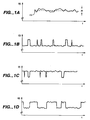
- Figures 1A-D show examples of noisy response in measured current of a memory cell.
- Figures 2A-C are schematic representations of an interface state trap in a floating gate memory cell.
- FIG. 3 shows one simplified embodiment of the present invention.
- Figures 4 A-D show a particular embodiment of a memory cell structure.
- Figures 5 A-C is a depiction of two particular read processes.
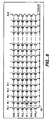
- Figure 6 shows another embodiment of a memory cell structure.
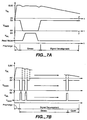
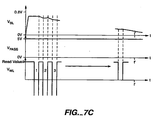
- Figures 7 A-C is a depiction of read processes for the structure of Figure 6 .
- non-volatile semiconductor memories has increased both by the reduction in the physical size of the individual components of the circuits including the memory cell and by increasing the amount of data storable in an individual memory cell.
- devices such as those described in U.S. patents 5,712,180 and 6,103,573 and U.S. patent US 6.426.893 and US 6.522.263 which are all assigned to SanDisk Corporation, can store four or more logical bits per physical floating gate storage transistor. In the case of 4 logical bits this storage will require each floating gate to be able to have encoded within it one of sixteen possible memory states.
- Each one of these memory states corresponds to a unique value, or, more accurately, a narrow range of values, of stored charge on the floating gate which is sufficiently separated from its neighboring states' charge storage range of values to clearly differentiate it from those neighboring states as well as all the other states. This is true for both a normal read operation as well as for a verify read done as part of a programming operation.
- Figures 1A-D illustrate examples of noise fluctuations in the reading of a memory cell.
- Figure 1A shows the case where the value of some parameter indicative of the state of the memory cell, in this case the current I ( t ) fluctuates around some mean value ⁇ I >.
- the signal development time is the time interval over which the measurable indicating the state of the cell is being developed.
- the measurable can be the cell drive current value, the cell threshold voltage, the bit line voltage drop generated in a fixed amount of time, or the amount of time required to generate a fixed amount of bit line voltage drop.
- Figures 1B and 1C show the example of the measured current from a memory cell where the current fluctuates around a value of, for example, 1 ⁇ A, but with a number of approximately equal magnitude spikes of, for example, 0.10 ⁇ A.
- the spikes are at a higher current from a base value
- the spikes are at a lower current
- the higher and lower conduction levels dictated by the noise source have comparable time characteristics. In all three cases their durations vary randomly.
- the time averaging effect of the integration time can be such that the impact of the noise becomes negligible.
- a memory cell can have noise with characteristic time constants that are comparable to or substantially longer than times that practical integration periods can span. In this situation, the noise can have an unacceptably large influence on the resulting sensing.
- V TH threshold voltage
- the gate/control gate voltage, V G can be swept to search for that value of V G which results in a pre-designated amount of drain to source current (for example 1 ⁇ A).
- a pre-designated amount of drain to source current for example 1 ⁇ A.
- V TH measurement is repeated many times, slightly different values of V TH from each measurement are found. It is also observed that using longer integration times and/or sweeping V G with smaller increments does not necessarily or appreciably reduce the noise.
- fixed voltages can be applied to all transistor terminals, to make numerous (e.g. thousands) of repetitive DC current measurements. Overall, the current remains roughly constant.
- At least one source of this noise could be interface state traps, IST.
- IST interface state traps
- interface state traps are being used loosely. Strictly speaking, what is here referred to as interface states include not just interface states located right at the interface of Si/SiO 2 , but also border traps that reside in the oxide and are within 30 ⁇ to 40 ⁇ of the interface. Electrically, both border states, and interface states (by the strict nomenclature) are switching states, whereas deep oxide traps are fixed states. Switching states can at times be occupied by an electron and at other times be empty, whereas fixed states have a tendency to retain their state over long periods of time at normal operating temperatures.
- V TH typically in the wide range from 400pA to 2 ⁇ A
- the source of the type of noise that the present invention addresses is frequently microscopic (e.g. single atom defects, interface traps, and dangling bonds---cf. Reference [2] of the Background section, p. 5060ff).
- the regions of influence of these microscopic defects are mesoscopic in the sense that the electric field lines emanating out of a charged trap site extend over mesoscopic distances (e.g. hundreds of Angstroms---cf. reference [3] of the Background section, Figure 4 , p. 1032).
- the effects of random trapping/de-trapping events become increasingly more prominent with the dimensions of devices becoming comparable to the mesoscopic dimensions of the regions of influence of these random microscopic phenomena.
- the memory cell By applying a varying signal, the memory cell is turned on much harder for shorter intervals than compared to DC sensing.
- the sensing signal is developed during the high values of the agitating stimulus, and during these short intervals the memory cell is turned on much harder by driving the cell into strong inversion.
- the charge density in the channel is higher in strong inversion. This means that the inversion layer charge can more effectively screen the field lines that emanate from a charged trap at or near the SiO2/Si interface.
- the stronger the inversion the thicker the inversion layer and the greater that component of the drain to source current which is flowing in deeper regions from the interface. These deeper currents are screened to greater extents from the random trapping/de-trapping events at the surface.
- Figures 2A and 2B are a simplified schematic representation of an interface state trap in a generic floating gate transistor. These figures show a floating gate memory from the side, in Figure 2A , and from the top, in Figure 2B . These show a control gate CG 201 placed over a floating gate 203, that is in turn over the channel of the substrate 205. When the source S and drain D are biased and a voltage is applied to the control gate, a current flows between the source and drain whose magnitude is determined by the amount of charge stored on the floating gate. When seen from above, the channel area under the pair of gates has a width W and a length L.
- the area between the floating gate FG 203 and the substrate 205 is occupied by the floating gate dielectric.
- the interface between the dielectric and the substrate results in a discontinuity of the structure on either side of the interface that can result in a site for an interface state trap.
- the density of distribution of such traps in the direction perpendicular to the surface is found to be roughly Gaussian and centered at the interface (see, for reference [4] of the Background section, Figure 2 ).
- a representation of one such a site is shown at 211 in Figures 2A and 2B .
- the effective channel width is reduced by an amount ⁇ W .
- the spikes correspond to the electron de-trapped state and the base current level to the trapped state.
- the lifetime of a trap is related to the distance of the trap site from the nearest conductor (cf. reference [1], Equation 5).
- the behavior of a given trap will depend on the bias conditions used to read the cell.
- the trap 211 is capacitively coupled to the source (S), drain (D), substrate (sub), and gate (G), where the coupling of the control gate is typically through an intermediary floating gate to the trap.
- the trap can be influenced to varying extents by changing the level on any of these terminals. Many effects of the traps can be modeled as conducting islands, such as are discussed more in reference [6].
- An exemplary embodiment applies an alternating voltage to one or more terminals of the device just prior to or during the signal development time (integration time) of the reading process.
- Other external agitations which are repeatable and whose average effect (from one integration time to the next integration time) remains constant may be used in other implementations.
- the well-known phenomenon of quantum tunneling is the mechanism responsible for the trapping/de-trapping action into deeper border traps whose communication to the nearest conductor is weak enough to warrant a charge localization effect.
- tunneling resistance has to be bigger than the quantum of resistance:
- Many of the deeper oxide traps are also less than 4nm away from the nearest conductor or semiconductor interface.
- Some examples of the nearest conductor/semiconductor interface are the channel, the floating gate bottom, or the select gate bottom.
- a time varying agitating signal may reduce noise if it manages to misalign the discrete energy state of the individual trap/defect/impurity from the Quasi-Fermi level (F N,P ) of the communication point of the nearest conductor by a few k B T in each cycle of the agitating signal, where k B is the Boltzman constant and T is the temperature. This is because if the energy required to transfer electrons across the barrier were smaller than k B T, then such a trap would have very short time constants, switching states many times during any given integration time, and thereby not contributing significantly to noise. This is based on the time averaging principle of Central Limit Theorem that will be elaborated upon later.
- the communication point of the nearest conductor is that point in the channel, floating gate, select gate, or control gate that is close enough to the trap such that electron tunneling can occur between the trap and that point. In most applications, an energy misalignment of ⁇ 3 k B T should be sufficient.
- the barrier is not thick enough or the energy barrier is not high enough (i.e. if the resistance is less than R Q ), then tunneling may not be the mechanism of the electron communication of the defect with the nearest electrode. This may be the case for the interface traps that are very close to the interface, or those that lie in the semiconductor side of the interface. It should also be noted that for such traps, even though there may exist no physical barrier that provides the high resistance, the energy barrier may be a result of the energy required to confine the charge to a potential well of atomic dimensions. In other words, there may not exist insulating atomic layer(s) between the defect, and the nearby electrode; but even in such a circumstance energy may be required to put an electron into the defect site, or to remove an electron from the defect site.
- this required energy may be a result of one or both of two distinct phenomena, namely size quantization, and charge quantization.
- Size quantization becomes prominent when the dimensions of a potential well become comparable to the Fermi wave length of the electrons in the well.
- capacitance can be used in a microscopic regime down to the atomic level as described in reference [7].
- capacitance can be defined as the amount of work per unit charge, ⁇ V, required to bring a fixed amount of charge, ⁇ Q, from the vacuum level to the system in question, as described in reference [7].
- control gate can be the electrode of choice for the application of the agitating AC signal.
- 1V amplitude AC signal applied to the control gate.
- 0.5V of amplitude is delivered to the floating gate (assuming a 50% control gate coupling ratio to the floating gate).
- the capacitive coupling ratio of floating gate to the trap that is modeled as a spherical conductor of 5 ⁇ radius is 10.4%.
- This result was obtained by a using 3D Poisson equation solver named "raphael" and distributed by Avanti Corporation.
- the capacitance of the trap to the channel was calculated to be 2.56 ⁇ 10 -19 F
- the capacitance of the trap to the floating gate was calculated to be 2.96 ⁇ 10 -20 F
- the total capacitance of the trap was calculated to be 2.85 ⁇ 10 -19 F.
- the 5 ⁇ radius of the trap is only an educated guess.
- the assumption that the relative permittivity of the oxide is a constant value of 3.9 may not be valid in the following sense: the few atomic layers between the trap and the channel may be composed of SiO x (as opposed to SiO 2 ). SiO x has less elemental oxygen than SiO 2 , having some oxygen vacancies. SiO x may have a different relative permittivity than SiO 2 . Moreover, Poisson Equation may lose its validity at such small dimensions. Using the above capacitance values results in only 50mV of a 1.0V control gate amplitude being delivered to the trap.
- episodic agitating stimuli that may have a net noise reduction effect include externally or internally produced photons, phonons, and magnetic fields.
- the sources of noise that this invention addresses are often microscopic in nature, including trap sites and atomic defects in any physical region of the device. Random electron/hole tunneling can change the state of a trap site. Depending on its position, the vacancy or occupancy of a trap will influence the device behavior. As devices are shrunk to mesoscopic dimensions and beyond, the effects of even a single trap become increasingly more prominent. In future generations these effects may become such a dominant part of the device behavior that even reliable binary operation of very small devices may not be possible.
- the time constants associated with the changing of the state of a trap is of the order of or longer than the signal integration time, then the random transitions of a trap between its states will be a source of noise.
- the trap is forced to make several independent decisions during each integration time. This can result in reduced device noise since each measurement will consist of several independent sub-measurements.
- an alternative to alternating rapidly between sub-measurements and agitating stimuli would be to wait for a period of time longer than the trap's characteristic time constants between any two sub-measurements. However, this wait may be prohibitively long in many instances.
- An exemplary embodiment consists of agitating the system during the integration time by applying a trapezoidal AC signal to the gate of an NMOS transistor.
- the effective integration time is confined to the time that the gate voltage is high. Due to the non-linear response of the transistor, during most of the fall time, all of the low time, and most of the rise time the gate voltage is below the threshold and the drain to source current is too low to contribute significantly to the average integrated current. For example, assume that for % of the integration time there is no current. To compensate for this and still maintain the same average current as in the standard DC case, during the high time the gate voltage can be increased so that high time current value is 4 times as large as the DC current value.
- the interface trap sites that contribute to noise behave as random, erratic micro-floating gates with memory like characteristics. If the tunneling resistance from the trap to the channel is high enough, then the average occupation/vacancy lifetime of the trapped charge(s) can be of the order of, or longer than, the integration time. In such a case, consecutive measurements may find the same value for the state of the cell. However, a measurement performed much later (with an intervening delay that is longer than the life time of the present occupation state of the trap) could find the state of the cell to be different. This same idea can be extended to a single signal development time (integration time corresponding to a single verify) in the following manner.
- multiple AC signals are applied to the control gate of a flash memory cell during a single integration time.
- the high value of these stimuli is slightly higher than the DC read voltage
- the low value is a number of volts lower than the high value
- the low value durations are sufficiently long so as to force the trap's occupation state into the vacant state, in effect randomizing the trap's occupation state during one high time from the trap's occupation state in the previous high time.
- a single signal development time will be composed of several sub-integration times (high times) during each of which the state of the trap is independent of the state of the trap during the previous sub-integration time.
- the purpose of the high times is to collectively develop the bit line voltage signal through the discharge of the bit line
- the purpose of the intervening low times is to de-correlate or randomize the trap's state during one high time from the trap's state during the next high time.
- the trap By the end of the low time the trap is forced into its vacant state, and upon the application of the high voltage value to the control gate the trap will make a new random decision to become occupied or to remain vacant. Because we are now only considering traps whose characteristic life times are comparable to or longer than the DC integration time, it is safe to assume that for these traps the state of the trap during each sub-integration time usually remains the same for the duration of that sub-integration time.
- the noise of the intra-cycle measurements remains correlated to the extent that the trapping/de-trapping life times are comparable to the up time of the signal.
- inter-cycle noise will be un-correlated as long as the low value is significantly lower than the high value and the low duration is comparable to the high duration.
- the distribution of multiple AC measurements of average currents, each of which is obtained by averaging current over 10 un-correlated AC cycles, will have a smaller variance when compared to the distribution of the same number of average DC current measurements, each of which has the same integration time as the AC case.
- the mean of A n is equal to ⁇
- the standard deviation of A n is equal to (1/ ⁇ n) ⁇ .
- a measurable that is composed of the averaging of, for example, 9 independent sub-measurements will have a standard deviation that will be 3 times smaller than the standard deviation inherent in the distribution of each of the sub-measurements.
- standard deviation and noise are interchangeable.
- the most central and the most effective concept presented here is the use of the ability to reduce noise by averaging over several independent sub-measurements.
- the voltage excursions (agitating stimuli) on any chosen electrode away from that electrode's DC read voltage will preferentially fill or empty the trap, depending on the sign of the excursions.
- the agitating stimuli can be applied to a selected word line, in which case the switch can be the existing drain side select gate, source side select gate, an unselected word line in the same segment, or a combination of the above.
- the agitating stimuli can be applied to a selected control gate (some times also referred to as the steering gate).
- the switch can be the select gate (i.e. word line), the transfer gate (the other control gate of a pair of floating gates, also known as the over drive steering gate), or both.
- either existing transistor(s) in the path of the current can be used as the mentioned switch(es), or new switching transistor(s) can be designed in to perform the task of shutting off the device current for the durations of the positive agitating stimuli.
- the RC time constants of the lines that deliver the agitating stimuli may be reduced by silicidation of poly-silicon lines, by converting typically poly-silicon lines to metal lines, or by reducing the local line segmentation lengths and delivering the agitating stimuli to only local segments (using local booster plates or booster lines which capacitively couple to the lines of interest). It has been found that noise can be reduced by the above method even though the effective integration time has been cut to a quarter of the DC integration time.
- a troublesome trap can either be occupied or vacant.
- ⁇ T is the average time from one tunneling-in event to another tunneling-in event, or from one tunneling-out event to another-tunneling out event.
- ⁇ T is the average time from one tunneling-in event to another tunneling-in event, or from one tunneling-out event to another-tunneling out event.
- the Fermi level of interest is the channel Fermi level at a point in the channel directly underneath the interface state.
- the trap energy level is below the Fermi level, then the trap is usually occupied, and occasionally becomes unoccupied. In such cases, the DC read current is at some base value most of the time with occasional short duration up-spikes. Alternatively, when the trap energy level is above the Fermi level, then the trap is usually unoccupied and occasionally becomes occupied. In such cases, the current is at some base value most of the time with occasional short duration down-spikes. The more energetically unfavorable it is for a trapping (or de-trapping) event to occur, the longer the lifetime of the initial de-trapped (or trapped) state.
- ⁇ E is composed of at least two components: 1) the electrostatic energy difference between before and after the transition, 2) the work expended by the power supplies to put an electron across a resistive tunnel barrier which has two different potentials at the two sides of the barrier.
- the electrostatic component of ⁇ E is much less than k B T, but the tunneling resistance R T is large, then the probability of tunneling per unit time is small and the life time of both the trapped, and the de-trapped states are long. In such cases, over long periods of time, the current is roughly half the time at some high value, and half the time at some low value with either frequent or infrequent transitions between the two values depending on the trap's tunneling resistance.
- the alternating signal can have a variety of different waveform shapes including, but not limited to, sinusoidal, rectangular, triangular, and trapezoidal.
- the combined periodic and non-periodic portions of voltage applied to a terminal may not have the same average value as the DC portion alone.
- Figure 3 schematically shows the example of the periodic disturbance (V per ) being applied to the gate along with a non-periodic voltage (V aper ).
- the combined waveform 307 may not be symmetric about the level (313) that would be used to measure the same data state without the AC portion.
- the combined waveform is arranged so that it is sufficiently high and low at the extreme peaks. Furthermore, an integer number of cycles of the periodic portion need not be used. As long as the waveform is reproducible for a given state that is to be measured and achieves the desired effect, it may be used.
- the exemplary embodiments use a waveform with a 50% duty cycle for de-correlating the reads as the main effect is at the bottom and top of the cycle. For this reason, it may be preferable to use a square or trapezoidal wave as these have a greater portion of their duty cycle at the peak levels when compared to a sinusoidal or triangular waveform.
- a square wave maximizes the peak values, in practice a square waveform suffers from overshoot (Gibbs phenomenon) that, particularly at the high end, can have undesirable effects in terms of reproducibility. Consequently, a trapezoidal waveform is often the best compromise.
- Figure 3 shows the stimulus applied to the gate for explicatory purposes
- other embodiments may apply the stimulus to another terminal.
- the voltage level at a trap can be affected by changing the voltage on any of the terminals of the cell that can deliver some portion of this voltage in a preferential manner to one of the two conducting entities on each side of the tunnel junction. For example, it may be applied to the substrate, allowing the stimulus to be applied to many cells simultaneously, and also avoids interfering with the read voltages applied to the gate. Other examples are discussed below for various cell embodiments.
- circuits that set the various voltages will be part of the decoders and circuit drivers that form the peripheral elements in the circuit array. These are described more fully in U.S. patents 5,172,338 and 5,272,669 and in U.S. patents 5,712,180 and 6,103,573 and U.S. patents US 6.426.893 and US6.512.265 , and are referred to below in relation to the multiple floating gate embodiment.
- the state of a storage unit can be determined using a number of different parameters.
- the determination of a cell's stored charge level can be performed by current sensing, where the magnitude of its conduction, using fixed bias conditions, is sensed. Alternately, such determination can be made through sensing threshold voltage, where the onset of such conduction is sensed using varied steering gate bias conditions.
- the determination could be performed dynamically by having the cells' charge-level determined driver-strength control the discharge rate of a dynamically held (by, e.g., a pre-charged capacitor) sense node. By sensing the time to reach a given discharge level, the stored charge level is determined. In this case, the parameter indicative of the cell's condition is a time.
- a dynamically held by, e.g., a pre-charged capacitor
- a binary search technique, or a slower linear search technique may be employed to find the state of the cell.
- a read operation will be composed of several verify operations. Each verify operation consists of applying a certain DC control gate voltage to the cell, and checking to see if the cell is ON or OFF at the applied control gate voltage value. A number of such verify operations done at intelligently chosen control gate values will then comprise the read operation. Each verify can be done in a number of different ways such as current sensing versus voltage sensing, dynamic sensing versus static sensing, and time to trip sensing versus fixed time sensing. Most of these variations have been discussed or referred to earlier. Dynamic-fixed-time-sensing would consist of the following sequence of events.
- each verify step of the read operation can be preceded by a single pulse agitating stimulus, or by multiple pulses of the agitating stimulus just prior to the start of the integration, that can be referred to as preconditioning.
- preconditioning single or multiple pulses of agitating stimuli can be applied during the integration time.
- Preconditioning alone, may have the following benefits.
- a single downward preconditioning voltage pulse may set most traps into their vacant state. If a greater majority of traps are such that under the DC read conditions their vacant state life times are longer than their occupied state life times, and also comparable to or longer than the integration time, then negative-going preconditioning pulse(s) may have an overall noise reducing effect. This may be the case for some insulating materials, and some typical DC read conditions.
- positive-going preconditioning pulse(s) may have an overall noise reducing effect. This may be the case for some insulating materials, and some typical DC read conditions. While there may be material tendencies in some cases favoring the negative-going preconditioning pulses, there always exist many exceptions to the rule. On the other hand, strong enough positive-going preconditioning pulse(s) may have an overall noise reducing effect because it (they) may go a long way towards recreating the historical conditions of the first verify right after a programming pulse.
- the ability to at least partially recreate the short term history conditions just prior to the first verify after the last programming pulse may reduce noise. From measurements over a rage of transistors covering various process technologies, it is observed that preconditioning is of limited effectiveness, and the most effective way of reducing noise is to apply multiple de-correlating pulses during each measurement such that each measurement is an average of multiple independent sub-measurements. The larger the number of independent sub-measurements contained within each measurement, the lower the noise associated with the measurement. As mentioned earlier, if N is the number of sub-measurements comprising each measurement, then the noise is reduced by a factor of (1/ ⁇ N).
- N 9 the amplitude of noise in measuring the VTH of a transistor can be reduced by a factor of 3, just based on the Central Limit Theorem. If a factor of 10 of noise reduction is required then N should be increased to a value of 100. As can be seen, this method of noise reduction can in some embodiments be more expensive in terms of both the energy consumed, and the time required to perform all these independent measurements.
- ECC Error Control Coding
- Identifying the address of the noisy cells allows the following two approaches to recovering the data: 1) With the knowledge of the noisy cell addresses, the ECC capabilities are dramatically increased by reducing the level of error correction required and redirecting these capabilities to error detection. 2) Different combinations of the neighboring data states of the noisy cells can be fed to the ECC engine until the ECC shows no errors. Gray scaling the states of a memory cell allows the neighbor states to any state to be different form that state by exactly 1 bit, further reducing burden on ECC due to nearest neighbor state transitions, as may be induced by cell noise.
- the various aspects of the present invention further extend the art in a number of additional ways: 1) cycling from inversion to accumulation is only a subset of the possible variety of voltage magnitudes and directions that can be applied as agitating stimulus; 2) a varying voltage is only one form of an agitating stimulus; 3) no specific practical noise reduction technique has been presented in the prior art, whereas the present patent invention presents a variety of detailed techniques that make the deployment of these and many other new ideas practical in, for example, non-volatile memories; 4) in none of the former art can one find the idea that the most powerful noise reduction effects can be achieved by the use of multiple agitating stimuli during a single integration time.
- a preferred embodiment uses a trapezoidal waveform whose low time, rise time, high time, and fall time are each a quarter of the period of the waveform.
- the high level of the signal is dictated by the V TH of the transistor and cannot exceed the V TH by much if the AC signal is being applied during the integration interval as this results in the transistor being fully on independent of its data state.
- Yet another embodiment that uses multiple pulses whose low value is the DC read value and whose high value is much higher can be applied within a single integration time.
- This gating element must be shut off in order to stop the otherwise excessive cell current during all those times when the gate voltage is driven well above the V TH of the cell.
- this gating element can be a non-selected word line within the selected NAND string, the source select transistor, or the drain (bit line) select transistor.
- the gating element can be the control (i.e. steering) gate of the non-selected floating gate in a storage unit or the select gate.
- This technique is a departure from the prevailing practice in the prior art of reducing noise by quieting down the system before and during the sensing.
- This technique allows for, and finds high levels of activity beneficial as long as the activity is always reproducible during each sensing period, or the period of the associated stimulus is much shorter than the integration time. If the episodic signal can be synchronized in a reproducible way with the integration interval, then the period of the signal can be enlarged to become comparable to the integration time. Synchronization can result in the percent high duration during an integration interval remaining constant across various integration intervals. It has been found that applying AC signals to the gate or the substrate of a transistor can significantly reduce noise. With AC waveforms that are synchronized to the integration interval, even one cycle per integration time has significantly reduced noise in many instances.
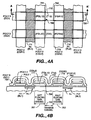
- Figures 4A and 4B show top and cross-sectional views, respectively, of one embodiment of a memory storage unit with multiple floating gates.
- a channel of the cell is formed between the two source/drain regions of bit-lines BL1 711 and BL2 712.
- the channel is subdivided into three regions: a left floating gate channel 761 under the left floating gate FGL12 781 and left control gate CGL2 771; a right floating gate channel 763 under the right floating gate FGR12 783 and right control gate CGR2 773; and, between these, a select channel 762 underneath the select transistor T12 772.
- the word-lines such as SG1 720
- the bit-lines such as BL1 711 and BL2 712
- the memory cell locations within the array are then defined by the intersection of these lines; for example, the cell of Figure 4B with select transistor T12 772 lies along word-lines SG1 720 between BL1 711 and BL2 712.
- the control gates are now connected along the columns parallel to the bit-lines instead of along the rows as in the more traditional architectures.
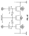
- Figure 4C is a circuit diagram depicting one embodiment of an array of memory cells such as those of Figures 4A and 4B , where Figure 4C is an equivalent circuit of these memory cells.
- the floating gates 781 and 783 of the cell can be programmed and read independently. More details on the operation of such a cell are provided in the references.
- interface state traps can be located anywhere along the channel at or proximate to the substrate-dielectric interface. This can be under either of the floating gates, under the select gate, or in the gaps between the gates, as with site 799 of Figure 4B . The site will be capacitively coupled with various strengths to all of the terminals of Figure 4C as well as to the substrate. In addition to stimulation by changing the level on the control (steering) gates, source, drain, and substrate, the introduction of a select gate provides another terminal to which an episodic stimulus can be applied.
- the direct capacitive coupling to select gate will be strongest for trap sites in the select channel region under the select gate, but will also affect sites in the floating gate channel, both through fringe field coupling and through the coupling of the site to the floating gate which is in turn capacitively coupled to the select gate (C 31L and C 31R in Figure 4C ). This is true also in single floating gate storage devices that include a select transistor.
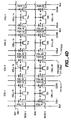
- the cells of Figures 4A-C are arranged in array such as that shown in Figure 4D .
- An exemplary embodiment applies an AC trapezoidal signal to the word lines (e.g. to 720) which is connected to the select gates (e.g. 772) or alternately applies the AC signal to the substrate instead of to the control (steering) gates (771 and 773).
- a modulation of the select gate voltage from a low value of 0V to a high value of 6V has been found to effect a reduction in noise in some cells.
- the conventional operating voltage of the word line is generally some fixed value, for example 5V, independent of cell data being read. This readily allows the application of a signal with a 6V amplitude with fixed high (6V) and low (0V) values.
- the control gate read voltage is data (state) dependent in many reading techniques, such as those described in the applications included by reference above. For states with low control gate threshold, a high amplitude AC signal results in the signal's low value becoming negative. This may be hard to implement in many devices and could possibly introduce disturbs.
- a non-volatile memory cell In sensing a non-volatile memory cell, whether as part of a read operation or as part of the verify phase of a program operation, there will typically be several phases. These include applying voltages to the cell so that it is biased appropriately for its data content to be sensed or measured, followed by an integration period that measures a parameter related to the state of the cell.
- the parameter In an EEPROM cell, the parameter is usually a voltage or the source-drain current, but can also be a time or frequency that is governed by the state of the cell.
- An example of one embodiment for the sense voltages of this measurement process is shown schematically in Figure 5A .
- Figure 5A shows the voltage level on a bit-line of a memory array, for example BLI 711 in Figure 4D .
- the first phase sets the gate voltages on the cells.
- the bit-lines of the cells to be read are charged up to a predetermined level.
- the voltage level on the bit-line is measured relative to a reference level V ref . If the voltage is at or above V ref , as in line 501, the cell is considered in an off state. If the voltage is below V ref , as in line 503, the cell is considered in an on state and that, consequently, the voltage on the control gate is above the threshold voltage of the cell.
- Figure 5B shows just the integration portion of Figure 5A , but with the inclusion of noise for the decay lines 501 and 503.
- the fluctuations due to noise can cause an erroneous reading at the time t ' if there is a fluctuation in a direction that would result in a mis-read.
- the lines 501 and 503 diverge with time, increasing the integration time will lead to greater separation, but at the expense of slower read times.
- the extent to which t' can be extended is limited as the voltages will eventually bottom out.
- An alternative approach, as described in the patent application entitled "Sense Amplifier for Multilevel Non-Volatile Integrated Memory Devices" is shown in Figure 5C .
- the cell is biased so that the trip point level V ref is at the same value as the precharge level of the second phase.
- the off state (501) continues to diverge from the on state (503) in time without both lines bottoming out.
- the on state will bottom out given enough integration time, and the off state will top out given enough integration time.
- the process described with respect to Figures 5A-C is just one of many reading techniques.
- the second, precharging phase of sensing may be combined with the first phase.
- both the parameter that is measured and how it is measured varies in different techniques.
- the measured parameter is a frequency indicative of total amount of current accumulated during the integration period.
- a single or periodic stimulus can be applied in one of the earlier phases of the read process so that the condition of the cell is randomized prior to beginning the integration phase. This could be done either prior to setting the gate voltages, or while the gate voltages are being set, or during the precharge phase, or some combination of these.
- the integration phase can then be executed without the concurrent exposure to the episodic stimulation.
- containing the stimulus entirely within the integration period can make it easier to reproduce the disturbance.
- a periodic voltage oscillation between channel turn on and shut off conditions could be applied to the select gate 772 for a predetermined number of cycles, for example n, during which time the total current flowing over the integration time interval is measured. This results in the read value corresponding to the integration of N independent sub-read values of shorter duration, matching the channel turn on intervals of the periodic voltage approach with the DC read conditions.
- FIG. 6 Another arrangement of floating gate memory cells is a NAND architecture, such as that described in U.S. patent US 2003 002348 .
- a NAND array is shown in Figure 6 that is adapted from this application. This figure shows columns of, in this example, four memory cells connected between a pair of select transistors to form the bit lines BL0 to BLN. Lines SGD_i and SGS_i are respectively connected to the drain and source select transistors of each column, and the control gates of the memory cells in each row are connected along a given word line WL_i.
- bit line BL1 is precharged to a level Y BL , the select transistors and non-selected word lines are set at a pass voltage V pass sufficient to turn all of the transistors in column 1 other than 601 fully on, and the selected word line WL1_i is set to a (here data dependent) read voltage V WL .
- the bit line BL1 then discharges at a rate determined by the data content of the storage element 601.
- a first set of embodiments uses pulses whose low value is the DC read value and whose high value is much higher can be applied within a single integration time. This gating element must be shut off in order to stop the otherwise excessive cell current during all those times when the gate voltage is driven well above the V TH of the cell.
- This gating element can be a non-selected word line within the NAND string of the column, the source select transistor, or the drain (bit line) select transistor. This is shown in Figures 7A and 7B .
- Figure 7A shows an episodic stimulus consisting of a single trapezoidal pulse applied on the single word line, corresponding to the voltage V WL .
- the selected word line is held at a normal read value during the precharge and signal development phases, with the stimulus applied during the stress period.
- the pulse reaches an exemplary value of 8V, a value the would turn the selected transistor on that word line fully on and rapidly discharge the bit line regardless of the data state stored on the transistor.
- the waveform V pass is applied to one of the other transistors in the column. By taking this other transistor to a voltage substantially below its threshold during the stress period, it is turned off and the bit line charge is maintained.
- the other transistors can be kept at the standard pass value, here 5V.
- V BL The resultant voltage on the bit line V BL is shown in the top waveform. It is initially precharged in this example to a value of 0.8V, at which point it begins to decay at a rate determined by the relation between the state of the selected cell and the read value on the bit line. V pass is then taken low, allowing V BL to remain steady, while V WL is stressed to 8V. The selected word line is then returned to its read value, V pass is returned to 5V, and the signal development is allowed to continue until the parameter value is latched at t' .
- Figure 7B is similar to Figure 7A , except now multiple pulses above the read voltage are applied to the word line. A corresponding set of dips in V pass is used to maintain the level on V BL while these pulses are applied.
- the resultant behavior on the bit line consists of the decay of V BL being broken up by a set of flat terraces when V pass is at 0V.
- Figure 7C shows an example of an alternate set of embodiments.
- the select transistors and all of the non-selected word lines are held on at the constant pass value of, here, 5V, as shown by the constant value of V pass .
- the stimulus on the selected word line is now a series of pulses taking V WL from the read value down to, for example, -6V.
- the resultant V BL waveform remains flat during the pulses, but no additional V pass signal is required since the stimulus does both jobs of applying the necessary stimulating voltage and conduction cutoff.
- Yet another application of this invention may be to produce more uniform conduction characteristics (e.g. subject to statistical variations of the threshold voltage V TH ) of very small transistors with prominent dopant fluctuation effects.
- the V TH of macroscopically identical transistors may be different because of microscopically varying dopant locations.
- the standard deviation of a sample of such V TH s obtained under DC conditions may be reduced by using the currently disclosed noise reduction technique.
- dopant fluctuation effects can give rise to excessive behavior variations across a collection of otherwise identical devices.
- An example would be increased spread in the threshold voltage of a collection of transistors that are meant to be identical.
- Dopant fluctuation effects increase as device sizes decrease to the point that there are few dopant atoms in the active portion of a device.
- externally applied alternating electric and magnetic fields may also be used to reduce noise.
- an alternating magnetic field could be used in a magnetic type memory cell, where it directly affects the cell, or even in a floating gate cell, where is could affect the cell through induced voltages.
- Increasing the temperature may have a 1/f' noise reduction effect but it will also increase thermal noise. Cycling through different temperatures may offer a method of reducing noise.
- the techniques of the present invention allow the steady state or DC characteristics of a memory cell to be read with reduced noise using a periodic or AC stimulus.
Landscapes
- Engineering & Computer Science (AREA)
- Computer Hardware Design (AREA)
- Computer Security & Cryptography (AREA)
- Non-Volatile Memory (AREA)
- Semiconductor Memories (AREA)
- Read Only Memory (AREA)
- Amplifiers (AREA)
- Bipolar Transistors (AREA)
Claims (32)
- Verfahren zum Betreiben eines nichtflüchtigen Speichers, umfassend:Anlegen eines Satzes von Spannungen (Vaper, Vper) an eine Speichereinheit (601) des nichtflüchtigen Speichers während eines Intervalls (t), undBestimmen der Leitungscharakteristika (I, VBL) der Speichereinheit in Reaktion auf den Satz von Spannungen,dadurch gekennzeichnet, dass
der Satz von Spannungen einen Lesespannungszustand (Vaper) sowie eine zeitlich variierende Anregungsstimulus(Vper)-Komponente, die sich von dem Lesespannungszustand unterscheidet, umfasst. - Verfahren nach Anspruch 1, wobei der Schritt des Bestimmens der Leitungscharakteristika das Messen einer Stromstärke, Spannung, Zeit und Frequenz umfasst.
- Verfahren nach Anspruch 1 oder Anspruch 2, wobei die Speichereinheit einen Floating-Gate-Transistor darstellt und der Satz von Spannungen ferner das Anlegen einer nichtperiodischen Spannung an ein erstes Steuergate (201, 771) des Transistors umfasst, wobei das Bestimmen der Leitungscharakteristika das Messen eines Parameters zwischen einem ersten und einem zweiten Source/Drain-Bereich (205) des Transistors während eines Leseintervalls umfasst.
- Verfahren nach Anspruch 3, wobei der episodische Stimulus an entweder das Steuergate des Transistors oder das Substrat des Transistors angelegt wird.
- Verfahren nach Anspruch 3 oder Anspruch 4, wobei der Floating-Gate-Transistor ferner ein Auswahlgate (772) umfasst und der episodische Stimulus an das Auswahlgate angelegt wird.
- Verfahren nach Anspruch 5, wobei der Floating-Gate-Transistor zwei Floating Gates aufweist, wobei ein erstes Steuergate (771) über dem ersten (781) der beiden Floating Gates angeordnet ist und ein zweites Steuergate (773) über dem zweiten (783) der beiden Floating Gates angeordnet ist, wobei das Auswahlgate (772) zwischen den beiden Steuergates liegt.
- Verfahren nach einem der Ansprüche 3 bis 6, wobei der Parameter entweder den Strom, der in einem Kanalbereich des Floating-Gate-Transistors fließt, oder eine Spannung, die zum Herstellen einer vorgegeben Stromstärke erforderlich ist, darstellt.
- Verfahren nach einem der Ansprüche 3 bis 7, wobei das Leseintervall eine erste Phase und eine darauffolgende zweite Phase umfasst, wobei die Messung eines Parameters während der zweiten Phase erfolgt und das Anlegen eines Satzes von Lesespannungswellenformen während der ersten Phase beginnt.
- Verfahren nach Anspruch 8, wobei der episodische Stimulus während entweder der ersten oder der zweiten Phase angelegt wird.
- Verfahren nach einem der Ansprüche 1 bis 8, wobei der episodische Stimulus eine Spannung darstellt, die entweder eine Sinuswellenform, eine Rechteckwellenform oder eine Trapezwellenform aufweist.
- Verfahren nach einem der vorhergehenden Ansprüche, wobei die Speichereinheit entweder eine magnetische Speicherzelle, bei welcher der episodische Stimulus ein Magnetfeld ist, eine Molekulartransistor-Speichereinheit, eine Einelektronentransistor-Speichereinheit oder eine Nanotransistor-Speichereinheit darstellt.
- Verfahren nach einem der vorhergehenden Ansprüche, wobei das Bestimmen der Leitungscharakteristika der Speichereinheit folgende Schritte umfasst:Bestimmen der Leitungscharakteristika der Speichereinheit unter Ansprechen auf den Satz von Spannungen zum ersten Mal; unddarauffolgendes Bestimmen der Leitungscharakteristika der Speichereinheit unter Ansprechen auf den Satz von Spannungen zum zweiten Mal, wobei die episodische Stimuluskomponente nur während der zweitmaligen Bestimmung angelegt wird.
- Verfahren nach Anspruch 12, wobei die nachfolgende zweitmalige Bestimmung der Leitungscharakteristika der Speichereinheit unter Ansprechen auf ein Ergebnis einer Fehlerkontrollcodierung erfolgt.
- Verfahren zum Lesen des Dateninhalts einer nichtflüchtigen Speichereinheit, umfassend:ein Verfahren entsprechend einem der vorhergehenden Ansprüche, wobei das Intervall ein Leseintervall darstellt,wobei die gemessene Charakteristik einen Parameterwert bemisst, der mit dem Dateninhalt der Speichereinheit während des Leseintervalls in Zusammenhang steht und den Beitrag einer Rauschkomponente umfasst, und
wobei der während des Leseintervalls an die Speichereinheit angelegte Pegel des Stimulus den Parameterwert beeinflusst, wodurch sich der Beitrag der Rauschkomponente reduziert. - Verfahren nach Anspruch 14, wobei die Speichereinheit einen Floating-Gate-Transistor darstellt und das Messen eines Parameterwertes das Anlegen einer nichtperiodischen Spannung an ein erstes Steuergate des Transistors umfasst, und wobei der Parameter zwischen einem ersten und einem zweiten Source/Drain-Bereich des Transistors gemessen wird.
- Verfahren nach Anspruch 15, wobei der episodische Stimulus entweder eine periodische Spannungswellenform oder einen einzelnen Spannungsimpuls darstellt.
- Verfahren nach Anspruch 16, wobei der episodische Stimulus eine periodische Spannungswellenform darstellt und wobei die periodische Spannung entweder eine Sinuswellenform, eine Rechteckwellenform oder eine Trapezwellenform aufweist.
- Verfahren nach Anspruch 16 oder Anspruch 17, wobei der episodische Stimulus eine periodische Spannungswellenform darstellt und wobei der Floating-Gate-Transistor ferner ein Auswahlgate umfasst und der episodische Stimulus an das Auswahlgate angelegt wird.
- Verfahren nach Anspruch 16 oder Anspruch 17, wobei der episodische Stimulus an das erste Steuergate des Transistors angelegt wird.
- Verfahren nach Anspruch 16 oder Anspruch 17, wobei der episodische Stimulus an das Substrat des Transistors angelegt wird.
- Verfahren nach einem der Ansprüche 14 bis 20, wobei das Anlegen eines episodischen Stimulus' unter Ansprechen auf ein Ergebnis einer Fehlerkontrollcodierung aufgerufen wird.
- Nichtflüchtiger Speicher, umfassend:eine Speichereinheit (601),einen Leseverstärker, der mit der Speichereinheit verbunden ist, um den Zustand der Speichereinheit unter Ansprechen auf einen Satz von Lesespannungen (Vaper, Vper) zu bestimmen, undTreiber, die mit der Speichereinheit verbunden sind, um den Satz von Lesespannungen an die Speichereinheit anzulegen,dadurch gekennzeichnet, dass der Satz von Lesespannungen umfasst:einen Lesespannungszustand (Vaper); undeinen zeitlich variierenden Stimulus-Spannungszustand (Vper), wobei sich der zeitlich variierende Stimulus-Spannungszustand von dem Lesespannungszustand unterscheidet.
- Speicher nach Anspruch 22, wobei der Leseverstärker durch Abfühlen einer Stromstärke oder einer Spannung arbeitet.
- Speicher nach Anspruch 22 oder Anspruch 23, wobei die Speichereinheit einen Floating-Gate-Transistor darstellt.
- Speicher nach Anspruch 24, wobei der episodische Stimulus-Spannungszustand an entweder ein Steuergate des Transistors oder das Substrat des Transistors angelegt wird.
- Speicher nach Anspruch 24, wobei der Floating-Gate-Transistor ferner ein Auswahlgate umfasst und der episodische Stimulus-Spannungszustand an das Auswahlgate angelegt wird.
- Speicher nach Anspruch 26, wobei der Floating-Gate-Transistor zwei Floating Gates aufweist, wobei das erste Steuergate (771) über einem ersten (781) der beiden Floating Gates angeordnet ist und ein zweites Steuergate (773) über dem zweiten (783) der beiden Floating Gates angeordnet ist, wobei das Auswahlgate (772) zwischen den beiden Steuergates liegt.
- Speicher nach einem der Ansprüche 22 bis 26, wobei der Parameter entweder den Strom, der in einem Kanalbereich des Floating-Gate-Transistors fließt, oder eine Spannung, die zum Herstellen einer vorgegebenen Stromstärke erforderlich ist, darstellt.
- Speicher nach einem der Ansprüche 22 bis 27, wobei der episodische Stimulus-Spannungszustand eine periodische Spannung darstellt, die entweder eine Rechteckwellenform oder eine Trapezwellenform aufweist.
- Speicher nach einem der Ansprüche 22 bis 29, der einen Fehlerkontrollcode-Abschnitt umfasst, der mit dem Leseverstärker und mit den Treibern gekoppelt ist, wobei die Treiber den episodischen Stimulus-Spannungszustand unter Ansprechen auf ein Steuersignal von dem Fehlerkontrollcode-Abschnitt anlegen.
- Speicher nach einem der Ansprüche 22 bis 30, wobei die Speichereinheit entweder eine magnetische Speicherzelle, bei welcher der episodische Stimulus ein Magnetfeld ist, eine Molekulartransistor-Speichereinheit, eine Einelektronentransistor-Speichereinheit oder eine Nanotransistor-Speichereinheit darstellt.
- Speicher nach einem der Ansprüche 22 bis 31, wobei der nichtflüchtige Speicher ein Array aus Speichereinheiten umfasst, ein Element dessen die Speichereinheit darstellt, und wobei er eine Verstärkerleitung umfasst, die zwischen einen der Treiber und einen Abschnitt des Arrays geschaltet ist, welcher die Speichereinheit umfasst, wodurch der episodische Stimulus-Spannungszustand angelegt wird.
Applications Claiming Priority (3)
| Application Number | Priority Date | Filing Date | Title |
|---|---|---|---|
| US10/052,924 US6850441B2 (en) | 2002-01-18 | 2002-01-18 | Noise reduction technique for transistors and small devices utilizing an episodic agitation |
| US52924 | 2002-01-18 | ||
| PCT/US2002/040204 WO2003063171A2 (en) | 2002-01-18 | 2002-12-16 | Noise reduction technique for transistors and small devices utilizing an episodic agitation |
Publications (2)
| Publication Number | Publication Date |
|---|---|
| EP1466331A2 EP1466331A2 (de) | 2004-10-13 |
| EP1466331B1 true EP1466331B1 (de) | 2008-02-13 |
Family
ID=21980791
Family Applications (1)
| Application Number | Title | Priority Date | Filing Date |
|---|---|---|---|
| EP02806618A Expired - Lifetime EP1466331B1 (de) | 2002-01-18 | 2002-12-16 | Rauschreduktionstechnik für transistoren und kleine anordnungen benutzend episodische agitation |
Country Status (10)
| Country | Link |
|---|---|
| US (3) | US6850441B2 (de) |
| EP (1) | EP1466331B1 (de) |
| JP (1) | JP4326339B2 (de) |
| KR (1) | KR100953373B1 (de) |
| CN (1) | CN100520980C (de) |
| AT (1) | ATE386328T1 (de) |
| AU (1) | AU2002357265A1 (de) |
| DE (1) | DE60225068T2 (de) |
| TW (1) | TWI264016B (de) |
| WO (1) | WO2003063171A2 (de) |
Families Citing this family (87)
| Publication number | Priority date | Publication date | Assignee | Title |
|---|---|---|---|---|
| US6805441B1 (en) * | 2003-08-11 | 2004-10-19 | Jorg Schuster | Rimless eyewear |
| US7046555B2 (en) | 2003-09-17 | 2006-05-16 | Sandisk Corporation | Methods for identifying non-volatile memory elements with poor subthreshold slope or weak transconductance |
| US7154779B2 (en) * | 2004-01-21 | 2006-12-26 | Sandisk Corporation | Non-volatile memory cell using high-k material inter-gate programming |
| DE102004029520B4 (de) * | 2004-06-18 | 2008-12-24 | Infineon Technologies Ag | Transistor-Anordnung mit Rauscherfassung |
| KR100602320B1 (ko) * | 2005-05-03 | 2006-07-18 | 주식회사 하이닉스반도체 | 프로그램 속도가 균일한 비휘발성 메모리 소자 |
| US20070059945A1 (en) * | 2005-09-12 | 2007-03-15 | Nima Mohklesi | Atomic layer deposition with nitridation and oxidation |
| KR100673020B1 (ko) * | 2005-12-20 | 2007-01-24 | 삼성전자주식회사 | 전계효과 소오스/드레인 영역을 가지는 반도체 장치 |
| US7412668B1 (en) * | 2006-01-30 | 2008-08-12 | Xilinx, Inc. | Integrated system noise management—decoupling capacitance |
| US7428717B1 (en) | 2006-01-30 | 2008-09-23 | Xilinx, Inc. | Integrated system noise management—system level |
| US7412673B1 (en) | 2006-01-30 | 2008-08-12 | Xilinx, Inc. | Integrated system noise management—bounce voltage |
| US7509608B1 (en) | 2006-01-30 | 2009-03-24 | Xilinx, Inc. | Integrated system noise management—clock jitter |
| US7499319B2 (en) * | 2006-03-03 | 2009-03-03 | Sandisk Corporation | Read operation for non-volatile storage with compensation for coupling |
| US7551486B2 (en) | 2006-05-15 | 2009-06-23 | Apple Inc. | Iterative memory cell charging based on reference cell value |
| US7852690B2 (en) * | 2006-05-15 | 2010-12-14 | Apple Inc. | Multi-chip package for a flash memory |
| US7911834B2 (en) * | 2006-05-15 | 2011-03-22 | Apple Inc. | Analog interface for a flash memory die |
| US7639542B2 (en) * | 2006-05-15 | 2009-12-29 | Apple Inc. | Maintenance operations for multi-level data storage cells |
| US7613043B2 (en) * | 2006-05-15 | 2009-11-03 | Apple Inc. | Shifting reference values to account for voltage sag |
| US7511646B2 (en) * | 2006-05-15 | 2009-03-31 | Apple Inc. | Use of 8-bit or higher A/D for NAND cell value |
| US8000134B2 (en) | 2006-05-15 | 2011-08-16 | Apple Inc. | Off-die charge pump that supplies multiple flash devices |
| US7568135B2 (en) | 2006-05-15 | 2009-07-28 | Apple Inc. | Use of alternative value in cell detection |
| US7701797B2 (en) * | 2006-05-15 | 2010-04-20 | Apple Inc. | Two levels of voltage regulation supplied for logic and data programming voltage of a memory device |
| US7639531B2 (en) * | 2006-05-15 | 2009-12-29 | Apple Inc. | Dynamic cell bit resolution |
| US7778072B2 (en) * | 2006-07-27 | 2010-08-17 | Macronix International Co., Ltd. | Method for fabricating charge-trapping memory |
| US7688366B2 (en) * | 2006-09-07 | 2010-03-30 | Aptina Imaging Corporation | Method and apparatus for suppressing noise in image sensor devices |
| US7646054B2 (en) | 2006-09-19 | 2010-01-12 | Sandisk Corporation | Array of non-volatile memory cells with floating gates formed of spacers in substrate trenches |
| US7696044B2 (en) | 2006-09-19 | 2010-04-13 | Sandisk Corporation | Method of making an array of non-volatile memory cells with floating gates formed of spacers in substrate trenches |
| US7800161B2 (en) * | 2006-12-21 | 2010-09-21 | Sandisk Corporation | Flash NAND memory cell array with charge storage elements positioned in trenches |
| US7642160B2 (en) * | 2006-12-21 | 2010-01-05 | Sandisk Corporation | Method of forming a flash NAND memory cell array with charge storage elements positioned in trenches |
| US7929349B2 (en) * | 2007-02-28 | 2011-04-19 | Samsung Electronics Co., Ltd. | Method of operating nonvolatile memory device |
| JP2008217971A (ja) * | 2007-02-28 | 2008-09-18 | Samsung Electronics Co Ltd | 不揮発性メモリ素子の作動方法 |
| US7904793B2 (en) * | 2007-03-29 | 2011-03-08 | Sandisk Corporation | Method for decoding data in non-volatile storage using reliability metrics based on multiple reads |
| US7797480B2 (en) * | 2007-03-29 | 2010-09-14 | Sandisk Corporation | Method for reading non-volatile storage using pre-conditioning waveforms and modified reliability metrics |
| US7966546B2 (en) * | 2007-03-31 | 2011-06-21 | Sandisk Technologies Inc. | Non-volatile memory with soft bit data transmission for error correction control |
| US7975209B2 (en) * | 2007-03-31 | 2011-07-05 | Sandisk Technologies Inc. | Non-volatile memory with guided simulated annealing error correction control |
| US7971127B2 (en) * | 2007-03-31 | 2011-06-28 | Sandisk Technologies Inc. | Guided simulated annealing in non-volatile memory error correction control |
| US7966550B2 (en) | 2007-03-31 | 2011-06-21 | Sandisk Technologies Inc. | Soft bit data transmission for error correction control in non-volatile memory |
| US7830729B2 (en) * | 2007-06-15 | 2010-11-09 | Micron Technology, Inc. | Digital filters with memory |
| US7733262B2 (en) | 2007-06-15 | 2010-06-08 | Micron Technology, Inc. | Quantizing circuits with variable reference signals |
| US7839703B2 (en) | 2007-06-15 | 2010-11-23 | Micron Technology, Inc. | Subtraction circuits and digital-to-analog converters for semiconductor devices |
| US7667632B2 (en) * | 2007-06-15 | 2010-02-23 | Micron Technology, Inc. | Quantizing circuits for semiconductor devices |
| US7818638B2 (en) * | 2007-06-15 | 2010-10-19 | Micron Technology, Inc. | Systems and devices including memory with built-in self test and methods of making and using the same |
| US7969783B2 (en) * | 2007-06-15 | 2011-06-28 | Micron Technology, Inc. | Memory with correlated resistance |
| US7538702B2 (en) * | 2007-06-15 | 2009-05-26 | Micron Technology, Inc. | Quantizing circuits with variable parameters |
| US8068367B2 (en) * | 2007-06-15 | 2011-11-29 | Micron Technology, Inc. | Reference current sources |
| US8117520B2 (en) * | 2007-06-15 | 2012-02-14 | Micron Technology, Inc. | Error detection for multi-bit memory |
| US7768868B2 (en) * | 2007-06-15 | 2010-08-03 | Micron Technology, Inc. | Digital filters for semiconductor devices |
| US7817073B2 (en) * | 2007-06-15 | 2010-10-19 | Micron Technology, Inc. | Integrators for delta-sigma modulators |
| US9135962B2 (en) | 2007-06-15 | 2015-09-15 | Micron Technology, Inc. | Comparators for delta-sigma modulators |
| KR101287447B1 (ko) * | 2007-08-28 | 2013-07-19 | 삼성전자주식회사 | 이이피롬 셀, 이이피롬 셀 제조 방법 및 이이피롬 셀에서의데이터 읽기 방법 |
| US8085596B2 (en) * | 2007-09-11 | 2011-12-27 | Micron Technology, Inc. | Reducing noise in semiconductor devices |
| US7952927B2 (en) * | 2007-12-05 | 2011-05-31 | Micron Technology, Inc. | Adjusting program and erase voltages in a memory device |
| US7864609B2 (en) * | 2008-06-30 | 2011-01-04 | Micron Technology, Inc. | Methods for determining resistance of phase change memory elements |
| JP5281455B2 (ja) | 2009-03-26 | 2013-09-04 | 株式会社東芝 | 不揮発性半導体記憶装置及びその駆動方法 |
| KR101586046B1 (ko) * | 2009-05-26 | 2016-01-18 | 삼성전자주식회사 | 저장 장치 및 그것의 읽기 방법 |
| JP5232729B2 (ja) * | 2009-06-30 | 2013-07-10 | 株式会社アドバンテスト | 出力装置および試験装置 |
| US8416624B2 (en) | 2010-05-21 | 2013-04-09 | SanDisk Technologies, Inc. | Erase and programming techniques to reduce the widening of state distributions in non-volatile memories |
| KR20120011642A (ko) | 2010-07-29 | 2012-02-08 | 삼성전자주식회사 | 기준 셀을 포함하는 불휘발성 메모리 장치 및 그것의 기준 전류 설정 방법 |
| US8432740B2 (en) | 2011-07-21 | 2013-04-30 | Sandisk Technologies Inc. | Program algorithm with staircase waveform decomposed into multiple passes |
| KR101874408B1 (ko) | 2011-11-09 | 2018-07-05 | 삼성전자주식회사 | 비휘발성 메모리 장치 및 이를 포함하는 메모리 시스템 |
| CN103177761A (zh) * | 2011-12-23 | 2013-06-26 | 北京大学 | 阻变存储设备及其操作方法 |
| US9190162B2 (en) * | 2012-03-13 | 2015-11-17 | Micron Technology, Inc. | Nonconsecutive sensing of multilevel memory cells |
| US8804430B2 (en) * | 2012-03-26 | 2014-08-12 | Sandisk Technologies Inc. | Selected word line dependent select gate diffusion region voltage during programming |
| US8638608B2 (en) | 2012-03-26 | 2014-01-28 | Sandisk Technologies Inc. | Selected word line dependent select gate voltage during program |
| US8750045B2 (en) | 2012-07-27 | 2014-06-10 | Sandisk Technologies Inc. | Experience count dependent program algorithm for flash memory |
| US8755228B2 (en) * | 2012-08-09 | 2014-06-17 | Kabushiki Kaisha Toshiba | Writing method of nonvolatile semiconductor memory device |
| US8780635B2 (en) * | 2012-11-09 | 2014-07-15 | Sandisk Technologies Inc. | Use of bloom filter and improved program algorithm for increased data protection in CAM NAND memory |
| US8773909B2 (en) * | 2012-11-09 | 2014-07-08 | Sandisk Technologies Inc. | CAM NAND with or function and full chip search capability |
| US8780634B2 (en) * | 2012-11-09 | 2014-07-15 | Sandisk Technologies Inc. | CAM NAND with OR function and full chip search capability |
| US8780633B2 (en) * | 2012-11-09 | 2014-07-15 | SanDisk Technologies, Inc. | De-duplication system using NAND flash based content addressable memory |
| US8811085B2 (en) * | 2012-11-09 | 2014-08-19 | Sandisk Technologies Inc. | On-device data analytics using NAND flash based intelligent memory |
| US8780632B2 (en) * | 2012-11-09 | 2014-07-15 | Sandisk Technologies Inc. | De-duplication techniques using NAND flash based content addressable memory |
| US9098403B2 (en) | 2012-11-09 | 2015-08-04 | Sandisk Technologies Inc. | NAND flash based content addressable memory |
| US8817541B2 (en) * | 2012-11-09 | 2014-08-26 | Sandisk Technologies Inc. | Data search using bloom filters and NAND based content addressable memory |
| US8634248B1 (en) * | 2012-11-09 | 2014-01-21 | Sandisk Technologies Inc. | On-device data analytics using NAND flash based intelligent memory |
| US8792279B2 (en) * | 2012-11-09 | 2014-07-29 | Sandisk Technologies Inc. | Architectures for data analytics using computational NAND memory |
| KR20140065244A (ko) * | 2012-11-21 | 2014-05-29 | 서울대학교산학협력단 | 랜덤텔레그래프 노이즈 영향을 억제하기 위한 반도체 소자에서의 읽기 방법 |
| KR102084461B1 (ko) | 2013-03-04 | 2020-04-14 | 삼성전자 주식회사 | 저항체를 이용한 비휘발성 메모리 장치 |
| US9075424B2 (en) | 2013-03-06 | 2015-07-07 | Sandisk Technologies Inc. | Compensation scheme to improve the stability of the operational amplifiers |
| US9380234B1 (en) * | 2015-05-01 | 2016-06-28 | Omnivision Technologies, Inc. | Reduced random telegraph signal noise CMOS image sensor and associated method |
| US9704588B1 (en) | 2016-03-14 | 2017-07-11 | Sandisk Technologies Llc | Apparatus and method for preconditioning currents to reduce errors in sensing for non-volatile memory |
| US9779832B1 (en) | 2016-12-07 | 2017-10-03 | Sandisk Technologies Llc | Pulsed control line biasing in memory |
| US10304550B1 (en) | 2017-11-29 | 2019-05-28 | Sandisk Technologies Llc | Sense amplifier with negative threshold sensing for non-volatile memory |
| US10643695B1 (en) | 2019-01-10 | 2020-05-05 | Sandisk Technologies Llc | Concurrent multi-state program verify for non-volatile memory |
| US10902920B2 (en) * | 2019-04-18 | 2021-01-26 | Micron Technology, Inc. | Driving conductors to target voltage levels |
| CN110610022B (zh) * | 2019-08-06 | 2021-11-19 | 华中科技大学 | 一种基于铁磁材料的电子模拟积分器 |
| US11024392B1 (en) | 2019-12-23 | 2021-06-01 | Sandisk Technologies Llc | Sense amplifier for bidirectional sensing of memory cells of a non-volatile memory |
| CN116720467B (zh) * | 2023-05-26 | 2026-07-21 | 上海交通大学 | 一种小尺寸半导体器件闪烁噪声的建模方法 |
Family Cites Families (19)
| Publication number | Priority date | Publication date | Assignee | Title |
|---|---|---|---|---|
| DE2828855C2 (de) * | 1978-06-30 | 1982-11-18 | Siemens AG, 1000 Berlin und 8000 München | Wortweise elektrisch umprogrammierbarer, nichtflüchtiger Speicher sowie Verfahren zum Löschen bzw. Einschreiben eines bzw. in einen solchen Speicher(s) |
| JPS5955071A (ja) | 1982-09-24 | 1984-03-29 | Hitachi Micro Comput Eng Ltd | 不揮発性半導体装置 |
| JP2645122B2 (ja) * | 1989-01-20 | 1997-08-25 | 株式会社東芝 | 不揮発性半導体メモリ |
| EP0935255A2 (de) | 1989-04-13 | 1999-08-11 | SanDisk Corporation | EEprom-System mit Blocklöschung |
| US5172338B1 (en) | 1989-04-13 | 1997-07-08 | Sandisk Corp | Multi-state eeprom read and write circuits and techniques |
| KR920010346B1 (ko) * | 1990-05-23 | 1992-11-27 | 삼성전자 주식회사 | 반도체 메모리의 센스앰프 구동회로 |
| DK0740854T3 (da) | 1991-08-29 | 2003-08-18 | Hyundai Electronics Ind | Automatisk justeret dual-bit split gate (DSG) flash EEPROM celle |
| US5712180A (en) | 1992-01-14 | 1998-01-27 | Sundisk Corporation | EEPROM with split gate source side injection |
| US6222762B1 (en) | 1992-01-14 | 2001-04-24 | Sandisk Corporation | Multi-state memory |
| US5798964A (en) | 1994-08-29 | 1998-08-25 | Toshiba Corporation | FRAM, FRAM card, and card system using the same |
| US5748533A (en) * | 1996-03-26 | 1998-05-05 | Invoice Technology, Inc. | Read circuit which uses a coarse-to-fine search when reading the threshold voltage of a memory cell |
| US5768192A (en) | 1996-07-23 | 1998-06-16 | Saifun Semiconductors, Ltd. | Non-volatile semiconductor memory cell utilizing asymmetrical charge trapping |
| JP3672384B2 (ja) * | 1996-07-24 | 2005-07-20 | 沖電気工業株式会社 | センス回路 |
| US5815438A (en) * | 1997-02-28 | 1998-09-29 | Advanced Micro Devices, Inc. | Optimized biasing scheme for NAND read and hot-carrier write operations |
| US5969986A (en) * | 1998-06-23 | 1999-10-19 | Invox Technology | High-bandwidth read and write architectures for non-volatile memories |
| US6044019A (en) | 1998-10-23 | 2000-03-28 | Sandisk Corporation | Non-volatile memory with improved sensing and method therefor |
| US6103573A (en) | 1999-06-30 | 2000-08-15 | Sandisk Corporation | Processing techniques for making a dual floating gate EEPROM cell array |
| US6275417B1 (en) * | 1999-10-08 | 2001-08-14 | Aplus Flash Technology, Inc. | Multiple level flash memory |
| US7111109B2 (en) * | 2002-03-13 | 2006-09-19 | Canon Kabushiki Kaisha | Control system, recording device and electronic apparatus |
-
2002
- 2002-01-18 US US10/052,924 patent/US6850441B2/en not_active Expired - Lifetime
- 2002-12-16 KR KR1020047011169A patent/KR100953373B1/ko not_active Expired - Fee Related
- 2002-12-16 EP EP02806618A patent/EP1466331B1/de not_active Expired - Lifetime
- 2002-12-16 AT AT02806618T patent/ATE386328T1/de not_active IP Right Cessation
- 2002-12-16 CN CNB028285190A patent/CN100520980C/zh not_active Expired - Fee Related
- 2002-12-16 AU AU2002357265A patent/AU2002357265A1/en not_active Abandoned
- 2002-12-16 WO PCT/US2002/040204 patent/WO2003063171A2/en not_active Ceased
- 2002-12-16 JP JP2003562940A patent/JP4326339B2/ja not_active Expired - Fee Related
- 2002-12-16 DE DE60225068T patent/DE60225068T2/de not_active Expired - Lifetime
- 2002-12-19 TW TW091136705A patent/TWI264016B/zh not_active IP Right Cessation
-
2004
- 2004-10-28 US US10/976,692 patent/US7092292B2/en not_active Expired - Lifetime
-
2006
- 2006-06-23 US US11/426,082 patent/US7403421B2/en not_active Expired - Lifetime
Also Published As
| Publication number | Publication date |
|---|---|
| US7092292B2 (en) | 2006-08-15 |
| WO2003063171A2 (en) | 2003-07-31 |
| CN100520980C (zh) | 2009-07-29 |
| JP2005520270A (ja) | 2005-07-07 |
| TWI264016B (en) | 2006-10-11 |
| ATE386328T1 (de) | 2008-03-15 |
| DE60225068T2 (de) | 2009-02-19 |
| DE60225068D1 (de) | 2008-03-27 |
| CN1623206A (zh) | 2005-06-01 |
| EP1466331A2 (de) | 2004-10-13 |
| US20050057979A1 (en) | 2005-03-17 |
| US7403421B2 (en) | 2008-07-22 |
| TW200302489A (en) | 2003-08-01 |
| JP4326339B2 (ja) | 2009-09-02 |
| US20030137877A1 (en) | 2003-07-24 |
| AU2002357265A1 (en) | 2003-09-02 |
| US6850441B2 (en) | 2005-02-01 |
| KR20040081462A (ko) | 2004-09-21 |
| KR100953373B1 (ko) | 2010-04-20 |
| US20060239079A1 (en) | 2006-10-26 |
| WO2003063171A3 (en) | 2003-12-31 |
Similar Documents
| Publication | Publication Date | Title |
|---|---|---|
| US7092292B2 (en) | Noise reduction technique for transistors and small devices utilizing an episodic agitation | |
| JP4800683B2 (ja) | 一列の電荷トラッピングメモリセルを作動させるための方法および装置 | |
| US7483307B2 (en) | Method and apparatus for sensing in charge trapping non-volatile memory | |
| JP2004152977A (ja) | 半導体記憶装置 | |
| US7321145B2 (en) | Method and apparatus for operating nonvolatile memory cells with modified band structure | |
| Diorio et al. | A complementary pair of four-terminal silicon synapses | |
| KR100706071B1 (ko) | 단일비트 비휘발성 메모리셀 및 그것의 프로그래밍 및삭제방법 | |
| JP2006338863A (ja) | 不揮発性電荷トラッピングメモリデバイスの動作方法およびプログラミング/消去の状態の決定方法 | |
| US7388785B2 (en) | Method for extracting the distribution of charge stored in a semiconductor device | |
| Woo et al. | Design of Superlattice Ferroelectric-Metal Field-effect Transistor for triple-level cell 3D NAND flash | |
| CN1941415A (zh) | 半导体元件 | |
| JP2005191542A (ja) | 半導体記憶装置 | |
| Karmakar | Design of multi-state dram using quantum dot gate non-volatile memory (qdnvm) | |
| Sikora et al. | Technologies and reliability of modern embedded flash cells | |
| Zambelli et al. | Reliability issues of NAND flash memories | |
| Lee et al. | Novel self-convergent scheme logic-process-based multilevel/analog EEPROM memory | |
| Wang | Electrical characterization of novel charge-trapping non-volatile semiconductor memory devices |
Legal Events
| Date | Code | Title | Description |
|---|---|---|---|
| PUAI | Public reference made under article 153(3) epc to a published international application that has entered the european phase |
Free format text: ORIGINAL CODE: 0009012 |
|
| 17P | Request for examination filed |
Effective date: 20040720 |
|
| AK | Designated contracting states |
Kind code of ref document: A2 Designated state(s): AT BE BG CH CY CZ DE DK EE ES FI FR GB GR IE IT LI LU MC NL PT SE SI SK TR |
|
| AX | Request for extension of the european patent |
Extension state: AL LT LV MK RO |
|
| 17Q | First examination report despatched |
Effective date: 20041018 |
|
| GRAP | Despatch of communication of intention to grant a patent |
Free format text: ORIGINAL CODE: EPIDOSNIGR1 |
|
| GRAS | Grant fee paid |
Free format text: ORIGINAL CODE: EPIDOSNIGR3 |
|
| GRAA | (expected) grant |
Free format text: ORIGINAL CODE: 0009210 |
|
| AK | Designated contracting states |
Kind code of ref document: B1 Designated state(s): AT BE BG CH CY CZ DE DK EE ES FI FR GB GR IE IT LI LU MC NL PT SE SI SK TR |
|
| RAP1 | Party data changed (applicant data changed or rights of an application transferred) |
Owner name: SANDISK CORPORATION |
|
| REG | Reference to a national code |
Ref country code: GB Ref legal event code: FG4D |
|
| REG | Reference to a national code |
Ref country code: CH Ref legal event code: EP |
|
| REG | Reference to a national code |
Ref country code: IE Ref legal event code: FG4D |
|
| REF | Corresponds to: |
Ref document number: 60225068 Country of ref document: DE Date of ref document: 20080327 Kind code of ref document: P |
|
| PG25 | Lapsed in a contracting state [announced via postgrant information from national office to epo] |
Ref country code: ES Free format text: LAPSE BECAUSE OF FAILURE TO SUBMIT A TRANSLATION OF THE DESCRIPTION OR TO PAY THE FEE WITHIN THE PRESCRIBED TIME-LIMIT Effective date: 20080524 Ref country code: FI Free format text: LAPSE BECAUSE OF FAILURE TO SUBMIT A TRANSLATION OF THE DESCRIPTION OR TO PAY THE FEE WITHIN THE PRESCRIBED TIME-LIMIT Effective date: 20080213 |
|
| PG25 | Lapsed in a contracting state [announced via postgrant information from national office to epo] |
Ref country code: AT Free format text: LAPSE BECAUSE OF FAILURE TO SUBMIT A TRANSLATION OF THE DESCRIPTION OR TO PAY THE FEE WITHIN THE PRESCRIBED TIME-LIMIT Effective date: 20080213 |
|
| PG25 | Lapsed in a contracting state [announced via postgrant information from national office to epo] |
Ref country code: BE Free format text: LAPSE BECAUSE OF FAILURE TO SUBMIT A TRANSLATION OF THE DESCRIPTION OR TO PAY THE FEE WITHIN THE PRESCRIBED TIME-LIMIT Effective date: 20080213 Ref country code: SI Free format text: LAPSE BECAUSE OF FAILURE TO SUBMIT A TRANSLATION OF THE DESCRIPTION OR TO PAY THE FEE WITHIN THE PRESCRIBED TIME-LIMIT Effective date: 20080213 |
|
| ET | Fr: translation filed | ||
| PG25 | Lapsed in a contracting state [announced via postgrant information from national office to epo] |
Ref country code: PT Free format text: LAPSE BECAUSE OF FAILURE TO SUBMIT A TRANSLATION OF THE DESCRIPTION OR TO PAY THE FEE WITHIN THE PRESCRIBED TIME-LIMIT Effective date: 20080714 Ref country code: CZ Free format text: LAPSE BECAUSE OF FAILURE TO SUBMIT A TRANSLATION OF THE DESCRIPTION OR TO PAY THE FEE WITHIN THE PRESCRIBED TIME-LIMIT Effective date: 20080213 Ref country code: SK Free format text: LAPSE BECAUSE OF FAILURE TO SUBMIT A TRANSLATION OF THE DESCRIPTION OR TO PAY THE FEE WITHIN THE PRESCRIBED TIME-LIMIT Effective date: 20080213 Ref country code: DK Free format text: LAPSE BECAUSE OF FAILURE TO SUBMIT A TRANSLATION OF THE DESCRIPTION OR TO PAY THE FEE WITHIN THE PRESCRIBED TIME-LIMIT Effective date: 20080213 Ref country code: SE Free format text: LAPSE BECAUSE OF FAILURE TO SUBMIT A TRANSLATION OF THE DESCRIPTION OR TO PAY THE FEE WITHIN THE PRESCRIBED TIME-LIMIT Effective date: 20080513 |
|
| PLBE | No opposition filed within time limit |
Free format text: ORIGINAL CODE: 0009261 |
|
| STAA | Information on the status of an ep patent application or granted ep patent |
Free format text: STATUS: NO OPPOSITION FILED WITHIN TIME LIMIT |
|
| 26N | No opposition filed |
Effective date: 20081114 |
|
| PG25 | Lapsed in a contracting state [announced via postgrant information from national office to epo] |
Ref country code: EE Free format text: LAPSE BECAUSE OF FAILURE TO SUBMIT A TRANSLATION OF THE DESCRIPTION OR TO PAY THE FEE WITHIN THE PRESCRIBED TIME-LIMIT Effective date: 20080213 Ref country code: BG Free format text: LAPSE BECAUSE OF FAILURE TO SUBMIT A TRANSLATION OF THE DESCRIPTION OR TO PAY THE FEE WITHIN THE PRESCRIBED TIME-LIMIT Effective date: 20080513 |
|
| PG25 | Lapsed in a contracting state [announced via postgrant information from national office to epo] |
Ref country code: CY Free format text: LAPSE BECAUSE OF FAILURE TO SUBMIT A TRANSLATION OF THE DESCRIPTION OR TO PAY THE FEE WITHIN THE PRESCRIBED TIME-LIMIT Effective date: 20080213 Ref country code: MC Free format text: LAPSE BECAUSE OF NON-PAYMENT OF DUE FEES Effective date: 20081231 |
|
| REG | Reference to a national code |
Ref country code: CH Ref legal event code: PL |
|
| PG25 | Lapsed in a contracting state [announced via postgrant information from national office to epo] |
Ref country code: IE Free format text: LAPSE BECAUSE OF NON-PAYMENT OF DUE FEES Effective date: 20081216 Ref country code: CH Free format text: LAPSE BECAUSE OF NON-PAYMENT OF DUE FEES Effective date: 20081231 Ref country code: LI Free format text: LAPSE BECAUSE OF NON-PAYMENT OF DUE FEES Effective date: 20081231 |
|
| PG25 | Lapsed in a contracting state [announced via postgrant information from national office to epo] |
Ref country code: LU Free format text: LAPSE BECAUSE OF NON-PAYMENT OF DUE FEES Effective date: 20081216 |
|
| PG25 | Lapsed in a contracting state [announced via postgrant information from national office to epo] |
Ref country code: TR Free format text: LAPSE BECAUSE OF FAILURE TO SUBMIT A TRANSLATION OF THE DESCRIPTION OR TO PAY THE FEE WITHIN THE PRESCRIBED TIME-LIMIT Effective date: 20080213 |
|
| PG25 | Lapsed in a contracting state [announced via postgrant information from national office to epo] |
Ref country code: GR Free format text: LAPSE BECAUSE OF FAILURE TO SUBMIT A TRANSLATION OF THE DESCRIPTION OR TO PAY THE FEE WITHIN THE PRESCRIBED TIME-LIMIT Effective date: 20080514 |
|
| REG | Reference to a national code |
Ref country code: NL Ref legal event code: SD Effective date: 20111229 |
|
| REG | Reference to a national code |
Ref country code: GB Ref legal event code: 732E Free format text: REGISTERED BETWEEN 20120112 AND 20120118 |
|
| REG | Reference to a national code |
Ref country code: FR Ref legal event code: TP Owner name: SANDISK TECHNOLOGIES INC., US Effective date: 20120229 |
|
| REG | Reference to a national code |
Ref country code: DE Ref legal event code: R082 Ref document number: 60225068 Country of ref document: DE Representative=s name: PATENTANWAELTE MAXTON LANGMAACK & PARTNER, DE |
|
| REG | Reference to a national code |
Ref country code: DE Ref legal event code: R082 Ref document number: 60225068 Country of ref document: DE Representative=s name: PATENTANWAELTE LIPPERT, STACHOW & PARTNER, DE Effective date: 20120713 Ref country code: DE Ref legal event code: R081 Ref document number: 60225068 Country of ref document: DE Owner name: SANDISK TECHNOLOGIES INC., US Free format text: FORMER OWNER: SANDISK CORP., MILPITAS, US Effective date: 20120713 Ref country code: DE Ref legal event code: R081 Ref document number: 60225068 Country of ref document: DE Owner name: SANDISK TECHNOLOGIES LLC, PLANO, US Free format text: FORMER OWNER: SANDISK CORP., MILPITAS, CALIF., US Effective date: 20120713 Ref country code: DE Ref legal event code: R082 Ref document number: 60225068 Country of ref document: DE Representative=s name: LIPPERT STACHOW PATENTANWAELTE RECHTSANWAELTE , DE Effective date: 20120713 Ref country code: DE Ref legal event code: R082 Ref document number: 60225068 Country of ref document: DE Representative=s name: PATENTANWAELTE MAXTON LANGMAACK & PARTNER, DE Effective date: 20120713 Ref country code: DE Ref legal event code: R081 Ref document number: 60225068 Country of ref document: DE Owner name: SANDISK TECHNOLOGIES INC., PLANO, US Free format text: FORMER OWNER: SANDISK CORP., MILPITAS, CALIF., US Effective date: 20120713 |
|
| PGFP | Annual fee paid to national office [announced via postgrant information from national office to epo] |
Ref country code: NL Payment date: 20131210 Year of fee payment: 12 Ref country code: FR Payment date: 20131209 Year of fee payment: 12 |
|
| PG25 | Lapsed in a contracting state [announced via postgrant information from national office to epo] |
Ref country code: IT Free format text: LAPSE BECAUSE OF NON-PAYMENT OF DUE FEES Effective date: 20081216 |
|
| REG | Reference to a national code |
Ref country code: DE Ref legal event code: R082 Ref document number: 60225068 Country of ref document: DE Representative=s name: PATENTANWAELTE LIPPERT, STACHOW & PARTNER, DE Ref country code: DE Ref legal event code: R082 Ref document number: 60225068 Country of ref document: DE Representative=s name: LIPPERT STACHOW PATENTANWAELTE RECHTSANWAELTE , DE |
|
| REG | Reference to a national code |
Ref country code: NL Ref legal event code: V1 Effective date: 20150701 |
|
| REG | Reference to a national code |
Ref country code: NL Ref legal event code: V1 Effective date: 20150701 |
|
| REG | Reference to a national code |
Ref country code: FR Ref legal event code: ST Effective date: 20150831 |
|
| PG25 | Lapsed in a contracting state [announced via postgrant information from national office to epo] |
Ref country code: NL Free format text: LAPSE BECAUSE OF NON-PAYMENT OF DUE FEES Effective date: 20150701 |
|
| PG25 | Lapsed in a contracting state [announced via postgrant information from national office to epo] |
Ref country code: FR Free format text: LAPSE BECAUSE OF NON-PAYMENT OF DUE FEES Effective date: 20141231 |
|
| REG | Reference to a national code |
Ref country code: DE Ref legal event code: R082 Ref document number: 60225068 Country of ref document: DE Representative=s name: PATENTANWAELTE LIPPERT, STACHOW & PARTNER, DE Ref country code: DE Ref legal event code: R081 Ref document number: 60225068 Country of ref document: DE Owner name: SANDISK TECHNOLOGIES LLC, PLANO, US Free format text: FORMER OWNER: SANDISK TECHNOLOGIES INC., PLANO, TEX., US Ref country code: DE Ref legal event code: R082 Ref document number: 60225068 Country of ref document: DE Representative=s name: LIPPERT STACHOW PATENTANWAELTE RECHTSANWAELTE , DE |
|
| PGFP | Annual fee paid to national office [announced via postgrant information from national office to epo] |
Ref country code: DE Payment date: 20171212 Year of fee payment: 16 |
|
| PGFP | Annual fee paid to national office [announced via postgrant information from national office to epo] |
Ref country code: GB Payment date: 20171213 Year of fee payment: 16 |
|
| REG | Reference to a national code |
Ref country code: DE Ref legal event code: R119 Ref document number: 60225068 Country of ref document: DE |
|
| GBPC | Gb: european patent ceased through non-payment of renewal fee |
Effective date: 20181216 |
|
| PG25 | Lapsed in a contracting state [announced via postgrant information from national office to epo] |
Ref country code: DE Free format text: LAPSE BECAUSE OF NON-PAYMENT OF DUE FEES Effective date: 20190702 |
|
| PG25 | Lapsed in a contracting state [announced via postgrant information from national office to epo] |
Ref country code: GB Free format text: LAPSE BECAUSE OF NON-PAYMENT OF DUE FEES Effective date: 20181216 |