EP1453077A2 - Rasterelektronenmikroskop und Probenbeobachtungsverfahren - Google Patents
Rasterelektronenmikroskop und Probenbeobachtungsverfahren Download PDFInfo
- Publication number
- EP1453077A2 EP1453077A2 EP03030029A EP03030029A EP1453077A2 EP 1453077 A2 EP1453077 A2 EP 1453077A2 EP 03030029 A EP03030029 A EP 03030029A EP 03030029 A EP03030029 A EP 03030029A EP 1453077 A2 EP1453077 A2 EP 1453077A2
- Authority
- EP
- European Patent Office
- Prior art keywords
- image
- sample
- focus
- electron microscope
- incident angle
- Prior art date
- Legal status (The legal status is an assumption and is not a legal conclusion. Google has not performed a legal analysis and makes no representation as to the accuracy of the status listed.)
- Withdrawn
Links
Images






Classifications
-
- H—ELECTRICITY
- H01—ELECTRIC ELEMENTS
- H01J—ELECTRIC DISCHARGE TUBES OR DISCHARGE LAMPS
- H01J37/00—Discharge tubes with provision for introducing objects or material to be exposed to the discharge, e.g. for the purpose of examination or processing thereof
- H01J37/02—Details
- H01J37/21—Means for adjusting the focus
-
- H—ELECTRICITY
- H01—ELECTRIC ELEMENTS
- H01J—ELECTRIC DISCHARGE TUBES OR DISCHARGE LAMPS
- H01J37/00—Discharge tubes with provision for introducing objects or material to be exposed to the discharge, e.g. for the purpose of examination or processing thereof
- H01J37/26—Electron or ion microscopes; Electron or ion diffraction tubes
- H01J37/28—Electron or ion microscopes; Electron or ion diffraction tubes with scanning beams
Definitions
- the present invention relates to a sample observation method using a scanning electron microscope and more particularly to a sample observation method suitable for the measurement of a height and the observation of a three-dimensional image in the dimension domain exceeding the focal depth of an electro-optic system.
- the stereoscopic observation method is a technique that gives a stereoscopic view of an image by combining plural sheets of images of different field-of-view angles in regard to the same field of view, and attains a measurement of the stereoscopic image.
- the stereoscopic observation method uses a shift of parallax of a corresponding point to attain the stereoscopic shape; however, since it is unable to recognize the shift of parallax satisfactorily in an out-of-focus domain, it is unable to attain the stereoscopic shape, which is a constraint of this method.
- the method attains the stereoscopic view by observing plural sheets of images measured with the tilt angle of a sample (or beam) varied, separately with right and left eyes by using various techniques.
- Patent Document 1
- Patent Document 2
- Non-patent Document 1
- Non-patent Document 2
- Non-patent Document 3
- Fig. 15 is an explanatory chart viewed from the sectional direction of a sample, which typically illustrates the formation of an image in viewing the scanning electron microscope image stereoscopically.
- the scanning electron microscope will be abbreviated to the SEM.
- Figs. 16A and 16B illustrate images by the SEM when the image is viewed stereoscopically under the condition of Fig. 15, in which Fig. 16A illustrates an image by the SEM when the sample or the incident electron is tilted by + ⁇ degree, and Fig. 16B illustrates an image by the SEM when the sample or the incident electron is tilted by - ⁇ degree.
- the method When irradiating an incident electron 151 to a sample 153 from the + ⁇ tilted direction, the method attains an image 161 on the monitor as illustrated in Fig. 16A.
- the method attains an image 162 on the monitor as illustrated in Fig. 16B.
- the domain corresponding to a domain 154 being in focus, illustrated in Fig. 15 is the domain 163.
- the depth of focus of the SEM is given by the following expression (1) (the non-patent document 1).
- f d min 2 V acc R min 2
- f d min represents the depth of focus
- V acc the accelerating voltage
- R min the resolution
- the depth of focus of the SEM becomes shallower as the resolution becomes higher.
- the in-focus domain is narrow. Accordingly, a trial for a stereoscopic view will attain only a part of the stereoscopic shape.
- the stereoscopic observation method using a recent high-resolution SEM has a narrow domain to give a stereoscopic view; that is, it is unable to attain correct height information only in a part of domain inside an image, which is a problem to be solved.
- the three-dimensional image observation method capable of attaining the stereoscopic shape and height difference distribution of an image to cover the whole domain.
- the invention intends, in answer to this demand, to provide a sample observation method capable of attaining the three-dimensional shape of a sample in a wider range.
- the observation method of the invention calculates heights (height differences) in the whole domain of an image, from plural sheets of images of different field-of-view angles, being in focus over the whole image, attained by means of the focal depth expanding function to thereby create a map (Z map) of the height information by each pixel; and displays a three-dimensional image as a bird's-eye view.
- the method also displays to superpose a Z map attained from image signals reflecting the composition information on a Z map attained from image signals reflecting the surface structure with different colors, which makes it possible to clearly understand the spatial distribution of a substance of unique composition inside the sample.
- the sample observation method using a scanning electron microscope includes the steps of: irradiating an electron beam to a sample at a first incident angle, and detecting a secondary signal (secondary electrons, reflection electrons, X-rays, etc.) emitted from the sample to capture a scanning electron microscope image of the sample; repeating the step while varying a focus in a step-wise manner, and capturing plural scanning electron microscope images at the first incident angle; irradiating the electron beam to the sample at a second incident angle different from the first incident angle, and detecting a secondary signal emitted from the sample to capture a scanning electron microscope image of the sample; repeating the step while varying a focus in a step-wise manner, and capturing plural scanning electron microscope images at the second incident angle; extracting most in-focus image domains from each of the plural scanning electron microscope images captured at the first incident angle, and creating a first all in-focus image being in focus over the whole image; extracting most in-focus image domains from each of the
- the sample observation method of the invention includes the steps of: calculating a distance between corresponding two pixels in the first all in-focus image and the second all in-focus image; calculating height information by each pixel on the basis of the distance between corresponding two pixels and a difference of angle between the first incident angle and the second incident angle; and creating a height map on the basis of the height information by each pixel.
- the height map is obtained, a three-dimensional bird's-eye view can be created from the map.
- the sample observation method using a scanning electron microscope includes the steps of: irradiating an electron beam to a sample at a first incident angle, and detecting first and second secondary signals emitted from the sample to capture a scanning electron microscope image of the sample based on the first secondary signal and a scanning electron microscope image of the sample based on the second secondary signal; repeating the step while varying a focus in a step-wise manner, and capturing plural scanning electron microscope images based on the first secondary signal and plural scanning electron microscope images based on the second secondary signal, at the first incident angle; irradiating the electron beam to the sample at a second incident angle different from the first incident angle, and detecting first and second secondary signals emitted from the sample to capture a scanning electron microscope image of the sample based on the first secondary signal and a scanning electron microscope image of the sample based on the second secondary signal; repeating the step while varying a focus in a step-wise manner, and capturing plural scanning electron microscope images based on the first secondary signal and plural scanning
- the first through fourth all in-focus images obtained may be arranged such that the first all in-focus image and the third all in-focus image are displayed with a first color, and the second all-in focus image and the fourth all in-focus image are displayed with a second color to observe a stereoscopic image.
- the sample observation method preferably includes the steps of: calculating a distance between corresponding two pixels in the first all in-focus image and the third all in-focus image; calculating height information of the sample based on the first secondary signal by each pixel, on the basis of the distance between corresponding two pixels in the first all in-focus image and the third all in-focus image and a difference of angle between the first incident angle and the second incident angle; creating a first height map on the basis of the height information of the sample based on the first secondary signal by each pixel; calculating a distance between corresponding two pixels in the second all in-focus image and the fourth all in-focus image; calculating height information of the sample based on the second secondary signal by each pixel, on the basis of the distance between corresponding two pixels in the second all in-focus image and the fourth all in-focus image and the difference of angle between the first incident angle and the second incident angle; and creating a second height map on the basis of the height information of the sample based on the second secondary signal by each pixel.
- the sample observation method preferably includes the steps of: creating a first three-dimensional bird's-eye view with a first display color from the first height map; creating a second three-dimensional bird's-eye view with a second display color different from the first display color from the second height map; and displaying to superpose the first three-dimensional bird's-eye view and the second three-dimensional bird's-eye view.
- the sample observation method may include a step of calculating a difference of height by each of corresponding pixels in the first height map and the second height map.
- the tilt angle of the sample to the irradiated electron beam may be varied by tilting the sample stage, or without tilting the sample stage, the angle of the irradiated electron beam falling on the sample may be varied by utilizing the deflection action occurring when passing the electron beam off the center of the objective lens of the scanning electron microscope. Tilting the relative angle between the electron beam and the sample by utilizing the deflection action of the objective lens will reduce a shift of the field of view occurring when shifting the sample stage.
- the scanning electron microscope includes: an electron beam source; an electro-optic system that scans to converge a primary electron beam emitted from the electron beam source on a sample, including an objective lens; an incident angle control means that controls an incident angle of the primary electron beam irradiated on the sample; a detector that detects a secondary signal emitted from the sample by the primary electron beam being irradiated on the sample; an all in-focus image processing means that extracts most in-focus image domains from each of the plural sample images of different focuses of the primary electron beam, and creates an all in-focus image being in focus over the whole image; and a calculation means that calculates height information of the sample by each pixel, on the basis of two all in-focus images created by the all in-focus image processing means at two different incident angles set by the incident angle control means, from the plural sample images of different focuses of the primary electron beam each captured at the two different incident angles.
- the incident angle control means may include a deflection means that deflects the primary electron beam at an objective point of the objective lens to make the electron beam fall on off the center of the objective lens.
- the scanning electron microscope may include an image display means that displays images, and a means that creates a three-dimensional bird's-eye view from the height information of the sample calculated by the calculation means, so that a created three-dimensional bird's-eye view can be displayed on the image display means.
- the scanning electron microscope may include a first detector that detects a first secondary signal and a second detector that detects a second secondary signal as the detector, so that the calculation means is able to calculate the height information of the sample based on the first secondary signal and the height information of the sample based on the second secondary signal.
- the first detector may be a secondary electron detector, for example
- the second detector may be a reflection electron detector, for example.
- the scanning electron microscope may include an image display means that displays images, and a means that creates a three-dimensional bird's-eye view from the height information of the sample calculated by the calculation means, so as to display a first three-dimensional bird' s-eye view created from the height information of the sample based on the first secondary signal and a second three-dimensional bird's-eye view created from the height information of the sample based on the second secondary signal on the display means.
- the first three-dimensional bird's-eye view and the second three-dimensional bird's-eye view are displayed with different colors.
- the domain giving the stereoscopic view is restricted because of the depth of focus of the scanning electron microscope; however, the method of the invention expands the domain to give the stereoscopic image, so that a three-dimensional shape can be attained in a wider rage. Due to insufficiency of the depth of focus, it has been difficult to calculate a height (height difference) from a domain being out of focus; however, a use of the method of this invention will allow calculating the height (height difference) from the whole domain of an image, so that the stereoscopic image can be displayed as a bird's-eye view. Further, by displaying to color-code different secondary signals and displaying to superpose two three-dimensional bird's-eye views, the difference in the height direction between objects displayed by the different signals can easily be measured.
- Fig. 1 illustrates a schematic configuration diagram as an example of the scanning electron microscope (SEM) according to the invention.
- SEM scanning electron microscope
- the primary electron beam 4 is converged by a convergent lens 5 (beam converging means) controlled by a power supply for lens control 21, and unnecessary parts of the primary electron beam are eliminated by a diaphragm 8. Thereafter, the primary electron beam 4 is converged as a minute spot on a sample 10 retained on a sample stage 15, by a convergent lens 6 (beam converging means) controlled by a power supply for second convergent lens control 22 and an objective lens 7 controlled by a power supply for objective lens control 23.
- the objective lens 7 may take on various configurations such as the in-lens system, out-lens system, or snorkel system (semi-in-lens system). Further, a retarding system is also possible which applies a negative voltage to the sample to decelerate the primary electron beam. Further, each lens may be an electrostatic lens configured with plural electrodes.
- a scan coil 9 scans the primary electron beam 4 on the sample 10 two-dimensionally.
- Secondary signals (sample signals) 12a, 12b of secondary electrons emitted from the sample 10 by the irradiation of the primary electron beam 4 advance above the objective lens 7; thereafter, the signals 12a, 12b are each separated according to the differences of energies by means for establishing orthogonally located electrical and magnetic fields for separating trajectory of secondary signal 11, and advance to the directions of secondary signal detectors 13a, 13b.
- These signals 12a, 12b are thereafter detected by the secondary signal detectors 13a, 13b.
- the signals from the secondary signal detectors 13a, 13b each pass signal amplifiers 14a, 14b, and are stored as image signals in an image memory for display 25. Image information stored in the image memory for display 25 is displayed on an image display 26 at any time.
- the signal flowing through the scan coil 9 is controlled according to the magnification in observation by a power supply for scan coil control 24.
- a two-stage deflecting coil 41 is disposed at the same position as the scan coil 9, and when tilting the beam, the deflecting coil 41 is able to two-dimensionally control the position of the primary electron beam 4 falling on the objective lens 7 by a power supply for tilt control 31, so that the object point of the objective lens 7 comes to the deflection point of support.
- an astigmatism correction coil 43 Near the convergent lens 6 is disposed an astigmatism correction coil 43, which is controlled to work with the condition of tilting the beam by a power supply for astigmatism correction 33.
- a two-stage deflecting coil 42 is disposed between the convergent lens 6 and the diaphragm 8, and the deflecting coil 42 is able to two-dimensionally control the position of the primary electron beam 4 falling on the convergent lens 6 by a power supply for astigmatism control 34, so that the object point of the convergent lens 6 comes to the deflection point of support.
- the operator is able to designate the condition of capturing images (scanning speed, accelerating voltage, etc.) and the condition of tilting the beam (tilt direction, tilt angle), and is also able to designate to output and/or save the images.
- the CPU 40 consecutively fetches plural images of different focuses, and calculates the focus control conditions thereof; and an image memory 32 stores them (image building means).
- the image data stored in the image memory 32 can be fetched from the SEM to the outside.
- the CPU 40 executes the image processing to the image data in the image memory 32, and synthesizes the data as the image having the depth of focus expanded; and the image memory 25 stores the data to display on the image display 26.
- the synthesized image (focal-depth-expanded image) can be stored also in the image memory 32, and the synthesized image data can be fetched from the SEM to the outside.
- the image processing is possible with a program stored in the CPU 40, and the processing can also be implemented at a high speed by means of a dedicated hardware. Since a high-speed image processing is possible with the dedicated hardware, while fetching the consecutive images of different focuses, the CPU 40 is also able to execute a sequential image processing in parallel, and to synthesize images of a large depth of focus.
- the image memory 32 is able to store multiple sheets of synthesized images (focal-depth-expanded images); and on the basis of the conditions of tilting the sample or the beam, it is possible to create Z maps, bird's-eye views, and color-coded displays of different signals (each will be described later) with a program stored in the CPU 40. It is also possible to store the created information in the image memory 25 as required, to display them on the image display 26, and to execute the image processing of creating sequential Z maps, bird's-eye views, and color-coded displays of different signals by means of the dedicated hardware.
- a common practice is to slant a sample stage.
- a deflecting coil 202 deflects a beam 201 at an object point on an objective lens 204, and makes the beam 201 fall on off the center of the objective lens 204, whereby the beam is tilted on a sample 207 by an angle ⁇ owing to the converging action of the objective lens 204.
- a position of an object point 205 viewed from the objective lens 204 does not move, if the beam is tilted, a field of view 206 will not move. In this state, it is only needed to attain the focal-depth-expanded images of different field-of-view angles.
- the stereoscopic observation method uses the focal depth expanding function as a means that captures the images being in focus on the whole image screen (Patent Document 1).
- the focal depth expanding function is an observation method that captures plural sheets of images of different focuses, executes position corrections and brightness corrections as needed, compares pixel information at the same position of the images, and extracts only the in-focus parts to thereby form a sheet of image.
- FE-SEM Field Emission SEM intended for high-magnification and high-resolution observations is unavoidable of insufficiency of the focal depth.
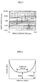
- Fig. 3 illustrates the relation between the resolution and the depth of focus of the FE-SEM in a high magnification. Fig. 3 shows that as the accelerating voltage is decreased and the resolution is increased, the depth of focus becomes shallower. As illustrated in Fig. 4, the depth of focus in a high magnification as mentioned here is defined as a distance (range) in the Z-direction, in which the resolution is maintained at 1.1 times of the highest resolution R min or lower in the variations of resolution to the optical axis Z near the focus point.
- the automatic expansion function of focal depth calculates the depth of focus in the current SEM condition in the first place, varies the focus by the depth of focus, and attains the SEM image.
- the breadth of varying the focus in each image is made equal to the depth of focus of the SEM.
- Non-patent Document 1 While executing this processing over the whole field of view of the SEM image, and finally joining up the pixels selected by the method so as to make a sheet of image, the method builds up the SEM image (focal-depth-expanded image) being in focus in the whole image (Non-patent Document 1, 2).
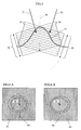
- Fig. 5 is an explanatory chart viewed from the sectional direction of a sample, which typically illustrates the formation of an image in viewing the SEM image stereoscopically by using the focal depth expanding function.
- Fig. 6 illustrates images when the images are viewed stereoscopically by using the focal depth expanding function, in which Fig. 6A illustrates a focal depth expanded image by the SEM when the sample or the incident electron is tilted by + ⁇ degree, and Fig. 6B illustrates a focal depth expanded image by the SEM when the sample or the incident electron is tilted by - ⁇ degree.
- the method attains an image 61 on the monitor of the SEM as illustrated in Fig. 6A.
- a focal depth 54 is confirmed to be deeper than a focal depth 56 when the focal depth expanding function is not used.
- the method attains an image 62 on the monitor of the SEM as illustrated in Fig. 6B.
- a focal depth 55 is confirmed to be deeper than a focal depth 57 when the focal depth expanding function is not used.
- both of the focal-depth-expanded image 61 by the SEM when the sample or the incident electron is tilted by + ⁇ degree and the focal-depth-expanded image 62 by the SEM when the sample or the incident electron is tilted by - ⁇ degree are confirmed to be in focus substantially on the whole image.
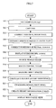
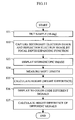
- Fig. 7 is a flow chart illustrating the procedure of capturing, synthesizing, and measuring images.
- step S11 tilts the sample or the beam incident direction by ⁇ degree
- step S12 captures images from the two directions by using the focal depth expanding function.
- step S13 automatically performs the position correction and brightness correction of the captured images.
- step S14 extracts only the in-focus parts of the corrected images and synthesizes them. These steps can be carried out automatically by using the focal depth expanding function.
- step S15 performs the position correction (adjusting the tilt center) of the two sheets of images captured by tilting the direction by ⁇ degree and using the focal depth expanding function
- step S16 gives a stereoscopic display.
- the tilt center is the point of reference for correcting the displacement of a tilted image.
- the sample or the electron beam is tilted; and at this moment, the field of view is moved by driving the stage or by shifting the beam so that the tilt center does not shift to the first sheet of the captured image.
- the numerical symbols 156, 165, 58, and 64 represent the sample tilt axis, and 166 and 65 the tilt center.
- step S17 performs the whole matching to the two sheets of images of different tilt angles captured by using the focal depth expanding function, detects the tilt centers between the two sheets of the images, and makes them coincident.
- step S18 performs the partial matching to a local image with one pixel as the center, between the two sheets of the images with the tilt centers coincident, and step S19 measures the shift length of the pixel between the two sheets of the images with the tilt centers coincident.
- tan ⁇ ⁇ /h
- Step S22 executes the above calculation to all the pixels over the whole domain of the image, and creates a height information map (Z map) by each pixel.
- the shift length of a small domain having one pixel on the center between two sheets of images can be calculated, for example, by correlating the images.
- the method of calculating the image correlation between two images 81, 82 will be described with Fig. 8.
- the method sets to the one image 81 a small frame 87 having a pixel on the center, of which shift length is to be calculated; and sets to the other image 82 a comparably large frame 88.
- the frame 88 set in the image 82 is to include the same part as the small frame 87 of the image 81.
- the method calculates the similarity of the images of small frames between the images 81, 82 by the correlation, and records the calculated values of the similarity as a map, as shown by 89 in Fig. 8C.
- the point giving the maximum similarity in the frame 88 is regarded as the same point. Executing the above calculation using a computer will automatically give the position of pixel in the image 82 corresponding to the center pixel of the small frame 87 in the image 81. Continuously executing this processing in the measurement domain will automatically give the shift length of the corresponding pixels in the two images 81, 82, and applying the calculated result to the above expressing (2) will give the height of each pixel.
- step S21 executes the evaluation of noises and matching errors as needed.
- step S22 creates the height information map (Z map) by each pixel.
- the Z map enables to display the height difference between arbitrary two points and the height distribution along an arbitrary straight line, and so forth.
- the Z map also allows displaying a stereoscopic image as a bird's-eye view (S23).
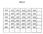
- Fig. 9 typically illustrates an example of the Z map. Each square in the drawing corresponds to the position of a pixel on the image, and the value h ij filled in the square represents the height of the sample in the pixel.
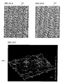
- Fig. 10 illustrates an example of the bird's-eye view created on the basis of a Z map.
- Fig. 10A illustrates an image attained by tilting the sample by + ⁇ degree and using the focal depth expanding function
- Fig. 10B illustrates an image attained by tilting the sample by - ⁇ degree and using the focal depth expanding function. Displaying these two sheets of images in a stereoscopic view and calculating the height of the whole image by each pixel will attain a Z map as illustrated in Fig. 9.
- To display the height information three-dimensionally according to the Z map will attain a bird's-eye view illustrated in Fig. 10C.
- Fig. 10C illustrates an image attained by rotating the three-dimensional map created from the images of Fig. 10A and Fig. 10B by 90°.
- the point 103 in Fig. 10C corresponds to the point 101 in Fig. 10A and the point 102 in Fig. 10B.
- step S31 tilts the sample or the beam incident direction by ⁇ degree
- step S32 captures a secondary electron image from the two directions by using the focal depth expanding function.
- step S32 captures a reflection electron image from the two directions by using the focal depth expanding function.
- the secondary electron image and reflection electron image may be captured at the same time.
- the position correction and brightness correction of the captured images are automatically carried out, and only the in-focus parts of the corrected images are extracted and synthesized.
- step S33 performs the position correction (adjusting the tilt center) of the two pairs of images captured by tilting the direction by ⁇ degree and using the focal depth expanding function, with regard to the secondary electron image and the reflection electron image each.
- step S34 measures the shift length by each pixel between the two sheets of images captured by tilting the direction by ⁇ degree and using the focal depth expanding function, with regard to the secondary electron image and the reflection electron image each.
- Step S35 calculates the height by each pixel from the measured shift length by each pixel and the tilt angle. Completing these steps will attain a Z map a ij of the secondary electron image as shown in Fig. 12A, and a Z map b ij of the reflection electron image as shown in Fig. 12B.
- the position correction of the two Z maps is unnecessary.
- the position adjustment of the two Z maps may be carried out by using the image correlation, or by designating through manual input from the images.
- step S37 displays to color-code and superpose the secondary electron image and the reflection electron image each, of which heights are calculated.
- this method it is possible to display a stereoscopic image with both the surface information by the secondary electrons and the composition information by the reflection electrons (electron signals emitted from the inside of the sample). It is also possible to quantitatively measure the depth from the surface observed by the secondary electron signals, the position at which the composition information by the reflection electrons exists.
- FIG. 13A illustrates a stereoscopic image created from a focal-depth-expanded image in the secondary electron mode of the sample
- Fig. 13B a stereoscopic image created from a focal-depth-expanded image in the reflection electron mode of the sample at the same position
- Fig. 13C a stereoscopic image having the two images superposed.
- these images are displayed on a paper, they are displayed as plane images on these drawings.
- the platinum catalyst particles carry extremely fine particles of platinum less than some nanometers on the carbon complex (or spongy structure) of fine particles less than some 10 nanometers.
- the secondary electron mode gives a clear observation to the surface shape of the carbon particles
- the reflection electron mode gives a clear observation to the dispersed state of platinum particles of the grain diameter less than about 10 nanometers.
- the superposition of the images may use a same color, or may arrange a specific color to each of the images.
- the image to be synthesized is not limited to the secondary electron image and the reflection electron image, and more than three sheets of images may be synthesized.
- Using the focal-depth-expanded image such as an X-ray analysis image (mapping image) will attain a three-dimensional distribution by each chemical element.
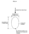
- the distance from the uppermost surface of the catalyst carrier (carbon) to the platinum particle lying on the backside of the catalyst carrier it is possible to measure the distance from the uppermost surface of the catalyst carrier (carbon) to the platinum particle lying on the backside of the catalyst carrier. That is, as shown in Fig. 14, the X-direction diameter of the catalyst carrier can be measured only from the uppermost information of the catalyst carrier, however the Y-direction diameter of the catalyst carrier can also be attained by measuring the distance to the platinum particle lying on the backside of the catalyst carrier.
- the area giving a stereoscopic view can be expanded, the three-dimensional shape can be attained in a wider range, and the height (height difference) can be calculated from the whole domain of the image, whereby the three-dimensional image can be displayed as a bird's-eye view. Also, by displaying to color-code and superpose plural three-dimensional bird's-eye views derived from different secondary signals, the difference in the height direction between objects displayed by the different signals can easily be attained.
Landscapes
- Chemical & Material Sciences (AREA)
- Analytical Chemistry (AREA)
- Analysing Materials By The Use Of Radiation (AREA)
- Length-Measuring Devices Using Wave Or Particle Radiation (AREA)
Applications Claiming Priority (2)
| Application Number | Priority Date | Filing Date | Title |
|---|---|---|---|
| JP2003000598 | 2003-01-06 | ||
| JP2003000598A JP2004214060A (ja) | 2003-01-06 | 2003-01-06 | 走査電子顕微鏡及びそれを用いた試料観察方法 |
Publications (1)
| Publication Number | Publication Date |
|---|---|
| EP1453077A2 true EP1453077A2 (de) | 2004-09-01 |
Family
ID=32767178
Family Applications (1)
| Application Number | Title | Priority Date | Filing Date |
|---|---|---|---|
| EP03030029A Withdrawn EP1453077A2 (de) | 2003-01-06 | 2003-12-30 | Rasterelektronenmikroskop und Probenbeobachtungsverfahren |
Country Status (3)
| Country | Link |
|---|---|
| US (1) | US6963067B2 (de) |
| EP (1) | EP1453077A2 (de) |
| JP (1) | JP2004214060A (de) |
Families Citing this family (34)
| Publication number | Priority date | Publication date | Assignee | Title |
|---|---|---|---|---|
| US6538249B1 (en) * | 1999-07-09 | 2003-03-25 | Hitachi, Ltd. | Image-formation apparatus using charged particle beams under various focus conditions |
| JP2005275199A (ja) * | 2004-03-26 | 2005-10-06 | Yokogawa Electric Corp | 3次元共焦点顕微鏡システム |
| JP4299195B2 (ja) * | 2004-06-28 | 2009-07-22 | 株式会社日立ハイテクノロジーズ | 荷電粒子線装置及びその光軸調整方法 |
| JP4695857B2 (ja) * | 2004-08-25 | 2011-06-08 | 株式会社日立ハイテクノロジーズ | 半導体検査方法および半導体検査装置 |
| JP4511303B2 (ja) * | 2004-10-05 | 2010-07-28 | 株式会社日立ハイテクノロジーズ | 荷電粒子線装置および寸法測定方法 |
| US7414252B2 (en) | 2004-11-03 | 2008-08-19 | Omniprobe, Inc. | Method and apparatus for the automated process of in-situ lift-out |
| WO2006113908A2 (en) * | 2005-04-20 | 2006-10-26 | The Regents Of The University Of California | Crytomography x-ray microscope stage |
| JP4533306B2 (ja) * | 2005-12-06 | 2010-09-01 | 株式会社日立ハイテクノロジーズ | 半導体ウェハ検査方法及び欠陥レビュー装置 |
| US20070237415A1 (en) * | 2006-03-28 | 2007-10-11 | Cao Gary X | Local Processing (LP) of regions of arbitrary shape in images including LP based image capture |
| JP2008084643A (ja) * | 2006-09-27 | 2008-04-10 | Fujitsu Ltd | 電子顕微鏡及び立体観察方法 |
| CZ2007510A3 (cs) | 2007-07-30 | 2008-01-30 | Tescan, S. R. O. | Zarízení pro prostorové zobrazování vzorku v reálném case |
| US8981294B2 (en) | 2008-07-03 | 2015-03-17 | B-Nano Ltd. | Scanning electron microscope, an interface and a method for observing an object within a non-vacuum environment |
| WO2010001399A1 (en) * | 2008-07-03 | 2010-01-07 | B-Nano | A scanning electron microscope, an interface and a method for observing an object within a non-vacuum environment |
| DE102008041070A1 (de) * | 2008-08-07 | 2010-02-11 | Robert Bosch Gmbh | Verfahren zur Bestimmung der Partikelhöhe |
| JP2012503856A (ja) | 2008-09-28 | 2012-02-09 | ビー−ナノ リミテッド | 真空化されたデバイス、および、走査型電子顕微鏡 |
| JP5249799B2 (ja) * | 2009-01-26 | 2013-07-31 | 浜松ホトニクス株式会社 | 画像出力システム、画像出力方法及び画像出力プログラム |
| JP5739119B2 (ja) * | 2009-09-15 | 2015-06-24 | 株式会社日立ハイテクサイエンス | 断面加工観察装置 |
| DE102009052392A1 (de) * | 2009-11-09 | 2011-12-15 | Carl Zeiss Nts Gmbh | SACP-Verfahren und teilchenoptisches System zur Ausführung eines solchen Verfahrens |
| JP5577977B2 (ja) * | 2010-09-16 | 2014-08-27 | 株式会社島津製作所 | 表面分析装置 |
| JP5331780B2 (ja) * | 2010-11-30 | 2013-10-30 | 株式会社日立ハイテクノロジーズ | 電子顕微鏡,電子顕微鏡用画像再構成システム、および電子顕微鏡用画像再構成方法 |
| JP5712074B2 (ja) | 2011-07-20 | 2015-05-07 | 株式会社日立ハイテクノロジーズ | 走査透過電子顕微鏡 |
| US8502146B2 (en) * | 2011-10-03 | 2013-08-06 | Kla-Tencor Corporation | Methods and apparatus for classification of defects using surface height attributes |
| JP6043528B2 (ja) * | 2012-07-20 | 2016-12-14 | 株式会社日立ハイテクノロジーズ | パターン測定装置 |
| JP2016513349A (ja) | 2013-02-20 | 2016-05-12 | ビー−ナノ リミテッド | 走査型電子顕微鏡 |
| WO2015068669A1 (ja) * | 2013-11-07 | 2015-05-14 | 株式会社日立ハイテクノロジーズ | 電子顕微鏡 |
| EP2879156A1 (de) * | 2013-12-02 | 2015-06-03 | Fei Company | Mikroskopie mit geladenen Teilchen mit erweiterter Elektronendetektion |
| US9218940B1 (en) * | 2014-05-30 | 2015-12-22 | Fei Company | Method and apparatus for slice and view sample imaging |
| US10410828B2 (en) * | 2014-12-22 | 2019-09-10 | Carl Zeiss Microscopy, Llc | Charged particle beam system and methods |
| CN108292580B (zh) * | 2015-12-03 | 2019-06-11 | 松定精度株式会社 | 荷电粒子线装置及扫描电子显微镜 |
| CN111354614B (zh) | 2016-01-29 | 2023-07-18 | 株式会社日立高新技术 | 带电粒子束装置及其光轴调整方法 |
| WO2019180760A1 (ja) * | 2018-03-19 | 2019-09-26 | 株式会社 日立ハイテクノロジーズ | パターン計測装置、及び計測を実行させるプログラムを記憶する非一時的なコンピュータ可読媒体 |
| LU100806B1 (en) * | 2018-05-30 | 2019-12-02 | Luxembourg Inst Science & Tech List | Joint nanoscale three-dimensional imaging and chemical analysis |
| JP6962897B2 (ja) * | 2018-11-05 | 2021-11-05 | 日本電子株式会社 | 電子顕微鏡および画像処理方法 |
| WO2023144909A1 (ja) * | 2022-01-26 | 2023-08-03 | 株式会社日立ハイテク | 異物高さの測定方法及び荷電粒子線装置 |
Family Cites Families (16)
| Publication number | Priority date | Publication date | Assignee | Title |
|---|---|---|---|---|
| NL8304217A (nl) * | 1983-12-07 | 1985-07-01 | Philips Nv | Automatisch instelbare electronenmicroscoop. |
| JPH01129113A (ja) * | 1987-11-16 | 1989-05-22 | Asahi Chem Ind Co Ltd | 表面粗さの測定方法 |
| JP2625787B2 (ja) * | 1987-12-18 | 1997-07-02 | 株式会社日立製作所 | 走査電子顕微鏡の立体計測較正方法 |
| JPH052362U (ja) * | 1991-02-25 | 1993-01-14 | サンユー電子株式会社 | ステレオ偏向システム |
| JPH05299048A (ja) * | 1992-04-24 | 1993-11-12 | Hitachi Ltd | 電子線装置および走査電子顕微鏡 |
| JP3109785B2 (ja) * | 1993-12-21 | 2000-11-20 | 株式会社日立製作所 | 走査電子顕微鏡の自動焦点合わせ装置 |
| JP3992848B2 (ja) * | 1998-07-21 | 2007-10-17 | 株式会社日立製作所 | 荷電粒子線装置 |
| US6353222B1 (en) * | 1998-09-03 | 2002-03-05 | Applied Materials, Inc. | Determining defect depth and contour information in wafer structures using multiple SEM images |
| JP3684943B2 (ja) | 1999-10-19 | 2005-08-17 | 株式会社日立製作所 | ビーム走査形検査装置 |
| US6538249B1 (en) * | 1999-07-09 | 2003-03-25 | Hitachi, Ltd. | Image-formation apparatus using charged particle beams under various focus conditions |
| JP3956584B2 (ja) | 2000-06-02 | 2007-08-08 | 株式会社日立製作所 | 全焦点画像合成方法及び装置 |
| JP4261743B2 (ja) * | 1999-07-09 | 2009-04-30 | 株式会社日立製作所 | 荷電粒子線装置 |
| JP4175597B2 (ja) * | 1999-11-30 | 2008-11-05 | 日本電子株式会社 | 走査電子顕微鏡 |
| JP4163373B2 (ja) | 2000-08-25 | 2008-10-08 | 株式会社日立製作所 | 電子線装置 |
| JP3951590B2 (ja) * | 2000-10-27 | 2007-08-01 | 株式会社日立製作所 | 荷電粒子線装置 |
| JP2002184336A (ja) | 2000-12-12 | 2002-06-28 | Hitachi Ltd | 荷電粒子線顕微鏡装置、荷電粒子線応用装置、荷電粒子線顕微方法、荷電粒子線検査方法、及び電子顕微鏡装置 |
-
2003
- 2003-01-06 JP JP2003000598A patent/JP2004214060A/ja active Pending
- 2003-12-30 EP EP03030029A patent/EP1453077A2/de not_active Withdrawn
-
2004
- 2004-01-05 US US10/750,838 patent/US6963067B2/en not_active Expired - Lifetime
Also Published As
| Publication number | Publication date |
|---|---|
| JP2004214060A (ja) | 2004-07-29 |
| US6963067B2 (en) | 2005-11-08 |
| US20040188611A1 (en) | 2004-09-30 |
Similar Documents
| Publication | Publication Date | Title |
|---|---|---|
| US6963067B2 (en) | Scanning electron microscope and sample observing method using it | |
| US8193494B2 (en) | Transmission electron microscope and method for observing specimen image with the same | |
| CN102484025B (zh) | 带电粒子束装置以及图像显示方法 | |
| US6531697B1 (en) | Method and apparatus for scanning transmission electron microscopy | |
| JP5302595B2 (ja) | 傾斜観察方法および観察装置 | |
| JP5183318B2 (ja) | 荷電粒子線装置 | |
| EP1238405B1 (de) | Verfahren und system zur untersuchung von substratoberflächen mittels teilchenstrahlapparat | |
| JP5735262B2 (ja) | 荷電粒子光学装置及びレンズ収差測定方法 | |
| JPH07192679A (ja) | 走査形電子顕微鏡 | |
| JPH05299048A (ja) | 電子線装置および走査電子顕微鏡 | |
| JP2005310602A (ja) | 荷電粒子線調整方法、及び荷電粒子線装置 | |
| CN109298001A (zh) | 电子束成像模块、电子束检测设备及其图像采集方法 | |
| JP2006032107A (ja) | 反射結像型電子顕微鏡及びそれを用いたパターン欠陥検査装置 | |
| US6677585B2 (en) | Scanning charged particle microscope, and focal distance adjusting method and astigmatism correction method thereof | |
| EP3379557A1 (de) | Raster-transmissionselektronenmikroskop und verfahren zur erfassung mit hohem durchsatz von elektronenstreuungswinkelverteilungsbildern | |
| JP2001210263A (ja) | 走査電子顕微鏡、そのダイナミックフォーカス制御方法および半導体デバイスの表面および断面形状の把握方法 | |
| KR102628711B1 (ko) | 하전 입자선 장치 | |
| JP4163373B2 (ja) | 電子線装置 | |
| JP4668807B2 (ja) | 荷電粒子線装置及び荷電粒子線画像生成方法 | |
| JP2006156134A (ja) | 反射結像型電子顕微鏡 | |
| JP2008282826A (ja) | 荷電粒子線調整方法、及び荷電粒子線装置 | |
| JP2000057987A (ja) | 形状観察用検出装置及び形状観察方法 | |
| JPH0636726A (ja) | 走査形顕微鏡 | |
| JP5500868B2 (ja) | 走査電子顕微鏡、および走査電子顕微鏡における像表示方法 | |
| JP5174498B2 (ja) | 荷電粒子ビーム装置 |
Legal Events
| Date | Code | Title | Description |
|---|---|---|---|
| PUAI | Public reference made under article 153(3) epc to a published international application that has entered the european phase |
Free format text: ORIGINAL CODE: 0009012 |
|
| AK | Designated contracting states |
Kind code of ref document: A2 Designated state(s): AT BE BG CH CY CZ DE DK EE ES FI FR GB GR HU IE IT LI LU MC NL PT RO SE SI SK TR |
|
| AX | Request for extension of the european patent |
Extension state: AL LT LV MK |
|
| 17P | Request for examination filed |
Effective date: 20060331 |
|
| STAA | Information on the status of an ep patent application or granted ep patent |
Free format text: STATUS: THE APPLICATION HAS BEEN WITHDRAWN |
|
| 18W | Application withdrawn |
Effective date: 20110311 |