EP1399269B1 - Waveform generator for microdeposition control system - Google Patents
Waveform generator for microdeposition control system Download PDFInfo
- Publication number
- EP1399269B1 EP1399269B1 EP02756113A EP02756113A EP1399269B1 EP 1399269 B1 EP1399269 B1 EP 1399269B1 EP 02756113 A EP02756113 A EP 02756113A EP 02756113 A EP02756113 A EP 02756113A EP 1399269 B1 EP1399269 B1 EP 1399269B1
- Authority
- EP
- European Patent Office
- Prior art keywords
- firing
- nozzles
- nozzle
- voltage
- microdeposition
- Prior art date
- Legal status (The legal status is an assumption and is not a legal conclusion. Google has not performed a legal analysis and makes no representation as to the accuracy of the status listed.)
- Expired - Lifetime
Links
Images


Classifications
-
- H—ELECTRICITY
- H01—ELECTRIC ELEMENTS
- H01L—SEMICONDUCTOR DEVICES NOT COVERED BY CLASS H10
- H01L21/00—Processes or apparatus adapted for the manufacture or treatment of semiconductor or solid state devices or of parts thereof
- H01L21/67—Apparatus specially adapted for handling semiconductor or electric solid state devices during manufacture or treatment thereof; Apparatus specially adapted for handling wafers during manufacture or treatment of semiconductor or electric solid state devices or components ; Apparatus not specifically provided for elsewhere
- H01L21/67005—Apparatus not specifically provided for elsewhere
- H01L21/67011—Apparatus for manufacture or treatment
- H01L21/6715—Apparatus for applying a liquid, a resin, an ink or the like
-
- H—ELECTRICITY
- H01—ELECTRIC ELEMENTS
- H01L—SEMICONDUCTOR DEVICES NOT COVERED BY CLASS H10
- H01L21/00—Processes or apparatus adapted for the manufacture or treatment of semiconductor or solid state devices or of parts thereof
- H01L21/02—Manufacture or treatment of semiconductor devices or of parts thereof
- H01L21/04—Manufacture or treatment of semiconductor devices or of parts thereof the devices having at least one potential-jump barrier or surface barrier, e.g. PN junction, depletion layer or carrier concentration layer
- H01L21/18—Manufacture or treatment of semiconductor devices or of parts thereof the devices having at least one potential-jump barrier or surface barrier, e.g. PN junction, depletion layer or carrier concentration layer the devices having semiconductor bodies comprising elements of Group IV of the Periodic System or AIIIBV compounds with or without impurities, e.g. doping materials
- H01L21/20—Deposition of semiconductor materials on a substrate, e.g. epitaxial growth solid phase epitaxy
-
- B—PERFORMING OPERATIONS; TRANSPORTING
- B25—HAND TOOLS; PORTABLE POWER-DRIVEN TOOLS; MANIPULATORS
- B25B—TOOLS OR BENCH DEVICES NOT OTHERWISE PROVIDED FOR, FOR FASTENING, CONNECTING, DISENGAGING OR HOLDING
- B25B11/00—Work holders not covered by any preceding group in the subclass, e.g. magnetic work holders, vacuum work holders
- B25B11/005—Vacuum work holders
-
- B—PERFORMING OPERATIONS; TRANSPORTING
- B29—WORKING OF PLASTICS; WORKING OF SUBSTANCES IN A PLASTIC STATE IN GENERAL
- B29C—SHAPING OR JOINING OF PLASTICS; SHAPING OF MATERIAL IN A PLASTIC STATE, NOT OTHERWISE PROVIDED FOR; AFTER-TREATMENT OF THE SHAPED PRODUCTS, e.g. REPAIRING
- B29C64/00—Additive manufacturing, i.e. manufacturing of three-dimensional [3D] objects by additive deposition, additive agglomeration or additive layering, e.g. by 3D printing, stereolithography or selective laser sintering
- B29C64/10—Processes of additive manufacturing
- B29C64/106—Processes of additive manufacturing using only liquids or viscous materials, e.g. depositing a continuous bead of viscous material
- B29C64/112—Processes of additive manufacturing using only liquids or viscous materials, e.g. depositing a continuous bead of viscous material using individual droplets, e.g. from jetting heads
-
- B—PERFORMING OPERATIONS; TRANSPORTING
- B29—WORKING OF PLASTICS; WORKING OF SUBSTANCES IN A PLASTIC STATE IN GENERAL
- B29C—SHAPING OR JOINING OF PLASTICS; SHAPING OF MATERIAL IN A PLASTIC STATE, NOT OTHERWISE PROVIDED FOR; AFTER-TREATMENT OF THE SHAPED PRODUCTS, e.g. REPAIRING
- B29C64/00—Additive manufacturing, i.e. manufacturing of three-dimensional [3D] objects by additive deposition, additive agglomeration or additive layering, e.g. by 3D printing, stereolithography or selective laser sintering
- B29C64/10—Processes of additive manufacturing
- B29C64/188—Processes of additive manufacturing involving additional operations performed on the added layers, e.g. smoothing, grinding or thickness control
-
- B—PERFORMING OPERATIONS; TRANSPORTING
- B41—PRINTING; LINING MACHINES; TYPEWRITERS; STAMPS
- B41J—TYPEWRITERS; SELECTIVE PRINTING MECHANISMS, i.e. MECHANISMS PRINTING OTHERWISE THAN FROM A FORME; CORRECTION OF TYPOGRAPHICAL ERRORS
- B41J2/00—Typewriters or selective printing mechanisms characterised by the printing or marking process for which they are designed
- B41J2/005—Typewriters or selective printing mechanisms characterised by the printing or marking process for which they are designed characterised by bringing liquid or particles selectively into contact with a printing material
- B41J2/01—Ink jet
- B41J2/015—Ink jet characterised by the jet generation process
- B41J2/04—Ink jet characterised by the jet generation process generating single droplets or particles on demand
- B41J2/045—Ink jet characterised by the jet generation process generating single droplets or particles on demand by pressure, e.g. electromechanical transducers
- B41J2/04501—Control methods or devices therefor, e.g. driver circuits, control circuits
- B41J2/04505—Control methods or devices therefor, e.g. driver circuits, control circuits aiming at correcting alignment
-
- B—PERFORMING OPERATIONS; TRANSPORTING
- B41—PRINTING; LINING MACHINES; TYPEWRITERS; STAMPS
- B41J—TYPEWRITERS; SELECTIVE PRINTING MECHANISMS, i.e. MECHANISMS PRINTING OTHERWISE THAN FROM A FORME; CORRECTION OF TYPOGRAPHICAL ERRORS
- B41J2/00—Typewriters or selective printing mechanisms characterised by the printing or marking process for which they are designed
- B41J2/005—Typewriters or selective printing mechanisms characterised by the printing or marking process for which they are designed characterised by bringing liquid or particles selectively into contact with a printing material
- B41J2/01—Ink jet
- B41J2/015—Ink jet characterised by the jet generation process
- B41J2/04—Ink jet characterised by the jet generation process generating single droplets or particles on demand
- B41J2/045—Ink jet characterised by the jet generation process generating single droplets or particles on demand by pressure, e.g. electromechanical transducers
- B41J2/04501—Control methods or devices therefor, e.g. driver circuits, control circuits
- B41J2/04506—Control methods or devices therefor, e.g. driver circuits, control circuits aiming at correcting manufacturing tolerances
-
- B—PERFORMING OPERATIONS; TRANSPORTING
- B41—PRINTING; LINING MACHINES; TYPEWRITERS; STAMPS
- B41J—TYPEWRITERS; SELECTIVE PRINTING MECHANISMS, i.e. MECHANISMS PRINTING OTHERWISE THAN FROM A FORME; CORRECTION OF TYPOGRAPHICAL ERRORS
- B41J2/00—Typewriters or selective printing mechanisms characterised by the printing or marking process for which they are designed
- B41J2/005—Typewriters or selective printing mechanisms characterised by the printing or marking process for which they are designed characterised by bringing liquid or particles selectively into contact with a printing material
- B41J2/01—Ink jet
- B41J2/015—Ink jet characterised by the jet generation process
- B41J2/04—Ink jet characterised by the jet generation process generating single droplets or particles on demand
- B41J2/045—Ink jet characterised by the jet generation process generating single droplets or particles on demand by pressure, e.g. electromechanical transducers
- B41J2/04501—Control methods or devices therefor, e.g. driver circuits, control circuits
- B41J2/0451—Control methods or devices therefor, e.g. driver circuits, control circuits for detecting failure, e.g. clogging, malfunctioning actuator
-
- B—PERFORMING OPERATIONS; TRANSPORTING
- B41—PRINTING; LINING MACHINES; TYPEWRITERS; STAMPS
- B41J—TYPEWRITERS; SELECTIVE PRINTING MECHANISMS, i.e. MECHANISMS PRINTING OTHERWISE THAN FROM A FORME; CORRECTION OF TYPOGRAPHICAL ERRORS
- B41J2/00—Typewriters or selective printing mechanisms characterised by the printing or marking process for which they are designed
- B41J2/005—Typewriters or selective printing mechanisms characterised by the printing or marking process for which they are designed characterised by bringing liquid or particles selectively into contact with a printing material
- B41J2/01—Ink jet
- B41J2/015—Ink jet characterised by the jet generation process
- B41J2/04—Ink jet characterised by the jet generation process generating single droplets or particles on demand
- B41J2/045—Ink jet characterised by the jet generation process generating single droplets or particles on demand by pressure, e.g. electromechanical transducers
- B41J2/04501—Control methods or devices therefor, e.g. driver circuits, control circuits
- B41J2/04558—Control methods or devices therefor, e.g. driver circuits, control circuits detecting presence or properties of a dot on paper
-
- B—PERFORMING OPERATIONS; TRANSPORTING
- B41—PRINTING; LINING MACHINES; TYPEWRITERS; STAMPS
- B41J—TYPEWRITERS; SELECTIVE PRINTING MECHANISMS, i.e. MECHANISMS PRINTING OTHERWISE THAN FROM A FORME; CORRECTION OF TYPOGRAPHICAL ERRORS
- B41J2/00—Typewriters or selective printing mechanisms characterised by the printing or marking process for which they are designed
- B41J2/005—Typewriters or selective printing mechanisms characterised by the printing or marking process for which they are designed characterised by bringing liquid or particles selectively into contact with a printing material
- B41J2/01—Ink jet
- B41J2/015—Ink jet characterised by the jet generation process
- B41J2/04—Ink jet characterised by the jet generation process generating single droplets or particles on demand
- B41J2/045—Ink jet characterised by the jet generation process generating single droplets or particles on demand by pressure, e.g. electromechanical transducers
- B41J2/04501—Control methods or devices therefor, e.g. driver circuits, control circuits
- B41J2/0456—Control methods or devices therefor, e.g. driver circuits, control circuits detecting drop size, volume or weight
-
- B—PERFORMING OPERATIONS; TRANSPORTING
- B41—PRINTING; LINING MACHINES; TYPEWRITERS; STAMPS
- B41J—TYPEWRITERS; SELECTIVE PRINTING MECHANISMS, i.e. MECHANISMS PRINTING OTHERWISE THAN FROM A FORME; CORRECTION OF TYPOGRAPHICAL ERRORS
- B41J2/00—Typewriters or selective printing mechanisms characterised by the printing or marking process for which they are designed
- B41J2/005—Typewriters or selective printing mechanisms characterised by the printing or marking process for which they are designed characterised by bringing liquid or particles selectively into contact with a printing material
- B41J2/01—Ink jet
- B41J2/015—Ink jet characterised by the jet generation process
- B41J2/04—Ink jet characterised by the jet generation process generating single droplets or particles on demand
- B41J2/045—Ink jet characterised by the jet generation process generating single droplets or particles on demand by pressure, e.g. electromechanical transducers
- B41J2/04501—Control methods or devices therefor, e.g. driver circuits, control circuits
- B41J2/04573—Timing; Delays
-
- B—PERFORMING OPERATIONS; TRANSPORTING
- B41—PRINTING; LINING MACHINES; TYPEWRITERS; STAMPS
- B41J—TYPEWRITERS; SELECTIVE PRINTING MECHANISMS, i.e. MECHANISMS PRINTING OTHERWISE THAN FROM A FORME; CORRECTION OF TYPOGRAPHICAL ERRORS
- B41J2/00—Typewriters or selective printing mechanisms characterised by the printing or marking process for which they are designed
- B41J2/005—Typewriters or selective printing mechanisms characterised by the printing or marking process for which they are designed characterised by bringing liquid or particles selectively into contact with a printing material
- B41J2/01—Ink jet
- B41J2/015—Ink jet characterised by the jet generation process
- B41J2/04—Ink jet characterised by the jet generation process generating single droplets or particles on demand
- B41J2/045—Ink jet characterised by the jet generation process generating single droplets or particles on demand by pressure, e.g. electromechanical transducers
- B41J2/04501—Control methods or devices therefor, e.g. driver circuits, control circuits
- B41J2/04575—Control methods or devices therefor, e.g. driver circuits, control circuits controlling heads of acoustic type
-
- B—PERFORMING OPERATIONS; TRANSPORTING
- B41—PRINTING; LINING MACHINES; TYPEWRITERS; STAMPS
- B41J—TYPEWRITERS; SELECTIVE PRINTING MECHANISMS, i.e. MECHANISMS PRINTING OTHERWISE THAN FROM A FORME; CORRECTION OF TYPOGRAPHICAL ERRORS
- B41J2/00—Typewriters or selective printing mechanisms characterised by the printing or marking process for which they are designed
- B41J2/005—Typewriters or selective printing mechanisms characterised by the printing or marking process for which they are designed characterised by bringing liquid or particles selectively into contact with a printing material
- B41J2/01—Ink jet
- B41J2/015—Ink jet characterised by the jet generation process
- B41J2/04—Ink jet characterised by the jet generation process generating single droplets or particles on demand
- B41J2/045—Ink jet characterised by the jet generation process generating single droplets or particles on demand by pressure, e.g. electromechanical transducers
- B41J2/04501—Control methods or devices therefor, e.g. driver circuits, control circuits
- B41J2/04581—Control methods or devices therefor, e.g. driver circuits, control circuits controlling heads based on piezoelectric elements
-
- B—PERFORMING OPERATIONS; TRANSPORTING
- B41—PRINTING; LINING MACHINES; TYPEWRITERS; STAMPS
- B41J—TYPEWRITERS; SELECTIVE PRINTING MECHANISMS, i.e. MECHANISMS PRINTING OTHERWISE THAN FROM A FORME; CORRECTION OF TYPOGRAPHICAL ERRORS
- B41J2/00—Typewriters or selective printing mechanisms characterised by the printing or marking process for which they are designed
- B41J2/005—Typewriters or selective printing mechanisms characterised by the printing or marking process for which they are designed characterised by bringing liquid or particles selectively into contact with a printing material
- B41J2/01—Ink jet
- B41J2/015—Ink jet characterised by the jet generation process
- B41J2/04—Ink jet characterised by the jet generation process generating single droplets or particles on demand
- B41J2/045—Ink jet characterised by the jet generation process generating single droplets or particles on demand by pressure, e.g. electromechanical transducers
- B41J2/04501—Control methods or devices therefor, e.g. driver circuits, control circuits
- B41J2/04588—Control methods or devices therefor, e.g. driver circuits, control circuits using a specific waveform
-
- B—PERFORMING OPERATIONS; TRANSPORTING
- B41—PRINTING; LINING MACHINES; TYPEWRITERS; STAMPS
- B41J—TYPEWRITERS; SELECTIVE PRINTING MECHANISMS, i.e. MECHANISMS PRINTING OTHERWISE THAN FROM A FORME; CORRECTION OF TYPOGRAPHICAL ERRORS
- B41J2/00—Typewriters or selective printing mechanisms characterised by the printing or marking process for which they are designed
- B41J2/005—Typewriters or selective printing mechanisms characterised by the printing or marking process for which they are designed characterised by bringing liquid or particles selectively into contact with a printing material
- B41J2/01—Ink jet
- B41J2/015—Ink jet characterised by the jet generation process
- B41J2/04—Ink jet characterised by the jet generation process generating single droplets or particles on demand
- B41J2/045—Ink jet characterised by the jet generation process generating single droplets or particles on demand by pressure, e.g. electromechanical transducers
- B41J2/04501—Control methods or devices therefor, e.g. driver circuits, control circuits
- B41J2/0459—Height of the driving signal being adjusted
-
- B—PERFORMING OPERATIONS; TRANSPORTING
- B41—PRINTING; LINING MACHINES; TYPEWRITERS; STAMPS
- B41J—TYPEWRITERS; SELECTIVE PRINTING MECHANISMS, i.e. MECHANISMS PRINTING OTHERWISE THAN FROM A FORME; CORRECTION OF TYPOGRAPHICAL ERRORS
- B41J2/00—Typewriters or selective printing mechanisms characterised by the printing or marking process for which they are designed
- B41J2/005—Typewriters or selective printing mechanisms characterised by the printing or marking process for which they are designed characterised by bringing liquid or particles selectively into contact with a printing material
- B41J2/01—Ink jet
- B41J2/015—Ink jet characterised by the jet generation process
- B41J2/04—Ink jet characterised by the jet generation process generating single droplets or particles on demand
- B41J2/045—Ink jet characterised by the jet generation process generating single droplets or particles on demand by pressure, e.g. electromechanical transducers
- B41J2/04501—Control methods or devices therefor, e.g. driver circuits, control circuits
- B41J2/04591—Width of the driving signal being adjusted
-
- B—PERFORMING OPERATIONS; TRANSPORTING
- B41—PRINTING; LINING MACHINES; TYPEWRITERS; STAMPS
- B41J—TYPEWRITERS; SELECTIVE PRINTING MECHANISMS, i.e. MECHANISMS PRINTING OTHERWISE THAN FROM A FORME; CORRECTION OF TYPOGRAPHICAL ERRORS
- B41J2/00—Typewriters or selective printing mechanisms characterised by the printing or marking process for which they are designed
- B41J2/005—Typewriters or selective printing mechanisms characterised by the printing or marking process for which they are designed characterised by bringing liquid or particles selectively into contact with a printing material
- B41J2/01—Ink jet
- B41J2/015—Ink jet characterised by the jet generation process
- B41J2/04—Ink jet characterised by the jet generation process generating single droplets or particles on demand
- B41J2/045—Ink jet characterised by the jet generation process generating single droplets or particles on demand by pressure, e.g. electromechanical transducers
- B41J2/04501—Control methods or devices therefor, e.g. driver circuits, control circuits
- B41J2/04593—Dot-size modulation by changing the size of the drop
-
- B—PERFORMING OPERATIONS; TRANSPORTING
- B41—PRINTING; LINING MACHINES; TYPEWRITERS; STAMPS
- B41J—TYPEWRITERS; SELECTIVE PRINTING MECHANISMS, i.e. MECHANISMS PRINTING OTHERWISE THAN FROM A FORME; CORRECTION OF TYPOGRAPHICAL ERRORS
- B41J2/00—Typewriters or selective printing mechanisms characterised by the printing or marking process for which they are designed
- B41J2/005—Typewriters or selective printing mechanisms characterised by the printing or marking process for which they are designed characterised by bringing liquid or particles selectively into contact with a printing material
- B41J2/01—Ink jet
- B41J2/015—Ink jet characterised by the jet generation process
- B41J2/04—Ink jet characterised by the jet generation process generating single droplets or particles on demand
- B41J2/045—Ink jet characterised by the jet generation process generating single droplets or particles on demand by pressure, e.g. electromechanical transducers
- B41J2/04501—Control methods or devices therefor, e.g. driver circuits, control circuits
- B41J2/04596—Non-ejecting pulses
-
- B—PERFORMING OPERATIONS; TRANSPORTING
- B41—PRINTING; LINING MACHINES; TYPEWRITERS; STAMPS
- B41J—TYPEWRITERS; SELECTIVE PRINTING MECHANISMS, i.e. MECHANISMS PRINTING OTHERWISE THAN FROM A FORME; CORRECTION OF TYPOGRAPHICAL ERRORS
- B41J3/00—Typewriters or selective printing or marking mechanisms characterised by the purpose for which they are constructed
- B41J3/407—Typewriters or selective printing or marking mechanisms characterised by the purpose for which they are constructed for marking on special material
-
- B—PERFORMING OPERATIONS; TRANSPORTING
- B41—PRINTING; LINING MACHINES; TYPEWRITERS; STAMPS
- B41J—TYPEWRITERS; SELECTIVE PRINTING MECHANISMS, i.e. MECHANISMS PRINTING OTHERWISE THAN FROM A FORME; CORRECTION OF TYPOGRAPHICAL ERRORS
- B41J3/00—Typewriters or selective printing or marking mechanisms characterised by the purpose for which they are constructed
- B41J3/54—Typewriters or selective printing or marking mechanisms characterised by the purpose for which they are constructed with two or more sets of type or printing elements
- B41J3/543—Typewriters or selective printing or marking mechanisms characterised by the purpose for which they are constructed with two or more sets of type or printing elements with multiple inkjet print heads
-
- H—ELECTRICITY
- H01—ELECTRIC ELEMENTS
- H01L—SEMICONDUCTOR DEVICES NOT COVERED BY CLASS H10
- H01L21/00—Processes or apparatus adapted for the manufacture or treatment of semiconductor or solid state devices or of parts thereof
- H01L21/67—Apparatus specially adapted for handling semiconductor or electric solid state devices during manufacture or treatment thereof; Apparatus specially adapted for handling wafers during manufacture or treatment of semiconductor or electric solid state devices or components ; Apparatus not specifically provided for elsewhere
- H01L21/67005—Apparatus not specifically provided for elsewhere
- H01L21/67011—Apparatus for manufacture or treatment
- H01L21/67098—Apparatus for thermal treatment
- H01L21/67103—Apparatus for thermal treatment mainly by conduction
-
- H—ELECTRICITY
- H01—ELECTRIC ELEMENTS
- H01L—SEMICONDUCTOR DEVICES NOT COVERED BY CLASS H10
- H01L21/00—Processes or apparatus adapted for the manufacture or treatment of semiconductor or solid state devices or of parts thereof
- H01L21/67—Apparatus specially adapted for handling semiconductor or electric solid state devices during manufacture or treatment thereof; Apparatus specially adapted for handling wafers during manufacture or treatment of semiconductor or electric solid state devices or components ; Apparatus not specifically provided for elsewhere
- H01L21/67005—Apparatus not specifically provided for elsewhere
- H01L21/67242—Apparatus for monitoring, sorting or marking
- H01L21/67248—Temperature monitoring
-
- H—ELECTRICITY
- H01—ELECTRIC ELEMENTS
- H01L—SEMICONDUCTOR DEVICES NOT COVERED BY CLASS H10
- H01L21/00—Processes or apparatus adapted for the manufacture or treatment of semiconductor or solid state devices or of parts thereof
- H01L21/67—Apparatus specially adapted for handling semiconductor or electric solid state devices during manufacture or treatment thereof; Apparatus specially adapted for handling wafers during manufacture or treatment of semiconductor or electric solid state devices or components ; Apparatus not specifically provided for elsewhere
- H01L21/683—Apparatus specially adapted for handling semiconductor or electric solid state devices during manufacture or treatment thereof; Apparatus specially adapted for handling wafers during manufacture or treatment of semiconductor or electric solid state devices or components ; Apparatus not specifically provided for elsewhere for supporting or gripping
- H01L21/6838—Apparatus specially adapted for handling semiconductor or electric solid state devices during manufacture or treatment thereof; Apparatus specially adapted for handling wafers during manufacture or treatment of semiconductor or electric solid state devices or components ; Apparatus not specifically provided for elsewhere for supporting or gripping with gripping and holding devices using a vacuum; Bernoulli devices
-
- H—ELECTRICITY
- H05—ELECTRIC TECHNIQUES NOT OTHERWISE PROVIDED FOR
- H05K—PRINTED CIRCUITS; CASINGS OR CONSTRUCTIONAL DETAILS OF ELECTRIC APPARATUS; MANUFACTURE OF ASSEMBLAGES OF ELECTRICAL COMPONENTS
- H05K3/00—Apparatus or processes for manufacturing printed circuits
- H05K3/10—Apparatus or processes for manufacturing printed circuits in which conductive material is applied to the insulating support in such a manner as to form the desired conductive pattern
- H05K3/12—Apparatus or processes for manufacturing printed circuits in which conductive material is applied to the insulating support in such a manner as to form the desired conductive pattern using thick film techniques, e.g. printing techniques to apply the conductive material or similar techniques for applying conductive paste or ink patterns
- H05K3/1241—Apparatus or processes for manufacturing printed circuits in which conductive material is applied to the insulating support in such a manner as to form the desired conductive pattern using thick film techniques, e.g. printing techniques to apply the conductive material or similar techniques for applying conductive paste or ink patterns by ink-jet printing or drawing by dispensing
- H05K3/125—Apparatus or processes for manufacturing printed circuits in which conductive material is applied to the insulating support in such a manner as to form the desired conductive pattern using thick film techniques, e.g. printing techniques to apply the conductive material or similar techniques for applying conductive paste or ink patterns by ink-jet printing or drawing by dispensing by ink-jet printing
-
- B—PERFORMING OPERATIONS; TRANSPORTING
- B41—PRINTING; LINING MACHINES; TYPEWRITERS; STAMPS
- B41J—TYPEWRITERS; SELECTIVE PRINTING MECHANISMS, i.e. MECHANISMS PRINTING OTHERWISE THAN FROM A FORME; CORRECTION OF TYPOGRAPHICAL ERRORS
- B41J2202/00—Embodiments of or processes related to ink-jet or thermal heads
- B41J2202/01—Embodiments of or processes related to ink-jet heads
- B41J2202/04—Heads using conductive ink
-
- B—PERFORMING OPERATIONS; TRANSPORTING
- B41—PRINTING; LINING MACHINES; TYPEWRITERS; STAMPS
- B41J—TYPEWRITERS; SELECTIVE PRINTING MECHANISMS, i.e. MECHANISMS PRINTING OTHERWISE THAN FROM A FORME; CORRECTION OF TYPOGRAPHICAL ERRORS
- B41J2202/00—Embodiments of or processes related to ink-jet or thermal heads
- B41J2202/01—Embodiments of or processes related to ink-jet heads
- B41J2202/09—Ink jet technology used for manufacturing optical filters
-
- H—ELECTRICITY
- H05—ELECTRIC TECHNIQUES NOT OTHERWISE PROVIDED FOR
- H05K—PRINTED CIRCUITS; CASINGS OR CONSTRUCTIONAL DETAILS OF ELECTRIC APPARATUS; MANUFACTURE OF ASSEMBLAGES OF ELECTRICAL COMPONENTS
- H05K1/00—Printed circuits
- H05K1/02—Details
- H05K1/0266—Marks, test patterns or identification means
- H05K1/0269—Marks, test patterns or identification means for visual or optical inspection
-
- H—ELECTRICITY
- H05—ELECTRIC TECHNIQUES NOT OTHERWISE PROVIDED FOR
- H05K—PRINTED CIRCUITS; CASINGS OR CONSTRUCTIONAL DETAILS OF ELECTRIC APPARATUS; MANUFACTURE OF ASSEMBLAGES OF ELECTRICAL COMPONENTS
- H05K2201/00—Indexing scheme relating to printed circuits covered by H05K1/00
- H05K2201/09—Shape and layout
- H05K2201/09818—Shape or layout details not covered by a single group of H05K2201/09009 - H05K2201/09809
- H05K2201/09918—Optically detected marks used for aligning tool relative to the PCB, e.g. for mounting of components
-
- H—ELECTRICITY
- H05—ELECTRIC TECHNIQUES NOT OTHERWISE PROVIDED FOR
- H05K—PRINTED CIRCUITS; CASINGS OR CONSTRUCTIONAL DETAILS OF ELECTRIC APPARATUS; MANUFACTURE OF ASSEMBLAGES OF ELECTRICAL COMPONENTS
- H05K3/00—Apparatus or processes for manufacturing printed circuits
- H05K3/0008—Apparatus or processes for manufacturing printed circuits for aligning or positioning of tools relative to the circuit board
Definitions
- the present invention relates to microdeposition systems, and more particularly to waveform generators for microdeposition systems for fabricating printed circuit boards, polymer light emitting diode (PLED) displays, and other devices requiring microdeposition of fluid.
- PLED polymer light emitting diode
- EP 0812 6 89 and EP 0895862 discloses systems and methods of driving a piezzo type ink jet head.
- microstructures that have small feature sizes on substrates.
- the microstructures form one of more layers of an electronic circuit.
- Examples of these structures include light-emitting diode (LED) display devices, polymer light-emitting diode (PLED) display devices, liquid crystal display (LCD) devices, printed circuit boards and the like.
- LED light-emitting diode
- PLED polymer light-emitting diode
- LCD liquid crystal display
- One technique for forming microstructures on a substrate includes screen printing.
- screen printing a fine mesh screen is positioned on the substrate. Fluid material is deposited through the screen and onto the substrate in a pattern defined by the screen. Screen printing requires contact between the screen and the substrate. Contact also occurs between the screen and the fluid material, which contaminates both the substrate and the fluid material.
- PLED polymer light-emitting diode
- Certain polymeric substances can be used in diodes to generate visible light of different wavelengths. Using these polymers, display devices having pixels with sub-components of red, green, and blue can be created.
- PLED fluid materials enable full-spectrum color displays and require very little power to emit a substantial amount of light. It is expected that PLED displays will be used in the future for various applications, including televisions, computer monitors, PDAs, other handheld computing devices, cellular phones, and the like. It is also expected that PLED technology will be used for manufacturing light-emitting panels that provide ambient lighting for office, storage, and living spaces.
- One obstacle to the widespread use of PLED display devices is the difficulty encountered to manufacture PLED display devices.
- Photolithography is another manufacturing technique that is used to manufacture microstructures on substrates. Photolithography is also not compatible with PLED display devices Manufacturing processes using photolithography generally involve the deposition of a photoresist material onto a substrate. The photoresist material is cured by exposure to light. A patterned mask is used to selectively apply light to the photo resist material. Photoresist that is exposed to the light is cured and unexposed portions are not cured. The uncured portions are removed from the substrate.
- An underlying surface of the substrate is exposed through the removed photoresist layer.
- the cured portions of the photoresist layer remain on the substrate.
- Another material is then deposited onto the substrate through the opened pattern on the photoresist layer, followed by the removal of the cured portion of the photoresist layer.
- Photolithography has been used successfully to manufacture many microstructures such as traces on circuit boards. However, photolithography contaminates the substrate and the material formed on the substrate. Photolithography is not compatible with the manufacture of PLED displays because the photoresist contaminates the PLED polymers. In addition, photolithography involves multiple steps for applying and processing the photoresist material. The cost of the photolithography process can be prohibitive when relatively small quantities are to be fabricated.
- Spin coating has also been used to form microstructures.
- Spin coating involves rotating a substrate while depositing fluid material at the center of the substrate. The rotational motion of the substrate causes the fluid material to spread evenly across the surface of the substrate.
- Spin coating is also an expensive process because a majority of the fluid material does not remain on the substrate.
- the size of the substrate is limited by the spin coating process to less than approximately 12", which makes spin coating unsuitable for larger devices such as PLED televisions.
- a microdeposition system and method includes a head with a plurality of nozzles.
- a controller generates nozzle firing commands that selectively fire the nozzles to create a desired feature pattern.
- Configuration memory stores voltage waveform parameters that define a voltage waveform for each of the nozzles.
- a digital to analog converter (DAC) sequencer communicates with the configuration memory and the controller and outputs a first voltage waveform for a first nozzle when a nozzle firing command for the first nozzle is received from the controller.
- a resistive ladder DAC receives the voltage waveforms from the DAC sequencer.
- An operational amplifier (opamp) communicates with the resistive ladder DAC and amplifies the voltage waveforms. The nozzles fire droplets when the voltage waveforms received from the opamp exceed a firing threshold of the nozzle.
- the nozzles include a common line and a nib line.
- the common line is connected to one of earth ground and a floating positive voltage relative to a system power ground.
- the opamp drives the nib line to a negative voltage that exceeds the firing threshold voltage to fire the nozzle.
- a first voltage waveform that is associated with a first nozzle includes at least one of a positive conditioning pulse and a negative conditioning pulse that does not exceed the firing threshold.
- the positive conditioning pulse or the negative conditioning pulse precedes or follows a firing pulse that exceeds the firing threshold.
- a configuration latch receives a set of voltage waveform parameters from the controller and loads the set of voltage waveform parameters in the configuration memory.
- a pixel latch communicates with the DAC sequencer and receives nozzle firing commands from the controller.
- the configuration memory stores a plurality of sets of voltage waveform parameters for each of the nozzles.
- a configuration set selector selects one of the sets of voltage waveform parameters based on operating conditions of the nozzle.
- FIG. 1 is a functional block diagram of a microdeposition system according to the present invention
- FIG. 2 is a functional block diagram of a controller for the microdeposition system of FIG. 1 ;
- FIG. 3 illustrates marks on a substrate that are used to position the microdeposition head
- FIG. 4 illustrates alignment of the head using optical character recognition and the marks
- FIG. 5 illustrates a nozzle of an exemplary microdeposition head
- FIG. 6 illustrates shearing of a piezo transducer during firing of the exemplary microdeposition head of FIG. 5 ;
- FIGs. 7 and 8 are exemplary cross-sections of monochrome and color polymer light emitting diodes (PLEDs);
- FIG. 9 illustrates controlled drying of a fluid material such as (PPV) polymer that has been deposited on a substrate
- FIG. 10 illustrates a manufacturing process for a printed circuit board according to the prior art
- FIG. 11 illustrates the use of the microdeposition system for depositing a resist fluid material onto a copper clad dielectric substrate for a printed circuit board
- FIG. 12 illustrates the use of the microdeposition system for depositing a conductive fluid material onto a dielectric substrate to create traces for a printed circuit board
- FIGs. 13A and 13B illustrate the microdeposition of resistive fluid materials to create resistors on printed circuit boards
- FIG. 14 illustrates the microdeposition of a capacitor
- FIG. 15 illustrates a printed circuit board replacement according to the present invention using a laminated insulator over microdeposited traces
- FIG. 16 illustrates a multilayer printed circuit board including internal microdeposited resistors, capacitors and/or traces;
- FIG. 17 illustrates a light panel including microdeposited pixels on a pixel plate and/or microdeposited fuses on an optional fuse plate;
- FIG. 18 illustrates a waveform generator that is capable of generating different firing waveforms for each nozzle
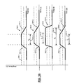
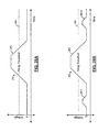
- FIG.19 illustrates rise slope, duration, timing and fall slope of an exemplary nozzle firing waveform
- FIG. 20 illustrates modification of rise slope, duration, timing and/or fall slope for several exemplary nozzle firing waveforms using the waveform generator of FIG. 18 ;
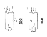
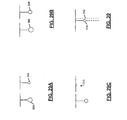
- FIG. 21 is a functional block diagram of a nozzle drive circuit according to the prior art.
- FIG. 22 is a functional block diagram of a nozzle drive circuit according to the present invention.
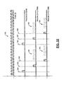
- FIG. 23 is a functional block diagram of an exemplary waveform generator
- FIG. 24 illustrates the configuration memory including one or more configuration sets
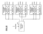
- FIG. 25 illustrates waveform timing adjustment using a pitch timing adjuster that adjusts waveform timing of the configuration sets
- FIG. 26 illustrates a waveform associated with an exemplary configuration set
- FIG. 27 illustrates an exemplary configuration set data structure
- FIG. 28A-28D illustrate exemplary waveforms associated with multiple configurations sets
- FIGs. 29A-29C illustrates drop formation analysis
- FIG. 30 illustrates drop alignment
- FIGs. 31A and 31B illustrates pitch adjustment of the microdeposition head
- FIG. 32 illustrates an exemplary use of over-clocking to adjust for pitch changes of the microdeposition head
- FIG. 33 illustrates an example of over-clocking to allow rapid nozzle firing and overlapping of the applied fluid material
- FIG. 34 illustrates overlapping droplets
- FIGs. 35A and 35B illustrate nozzle adjustments to provide uniform droplets
- FIG. 36 illustrates a diagonal feature that is created without over-clocking
- FIG. 37 illustrates a diagonal feature that is created with over-clocking
- FIG. 38 illustrates multiple microdeposition heads that are attached together to provide reduced pitch
- FIG. 39 illustrates multiple adjustable microdeposition heads that are attached together to provide adjustable pitch.
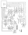
- a microdeposition system 20 is illustrated and includes a controller 22, a head assembly 24, and a substrate assembly 26.
- a rotational position or pitch of the head assembly 24 is adjusted using a rotary position motor 30 and a rotary position sensor 32.
- a height of the head assembly 24 relative to the substrate assembly 26 may be adjusted using a height adjustment motor 34 and a height sensor 36.
- a lateral position of the head assembly 24 is adjusted using a lateral position motor 40 and a lateral position sensor 42.
- a microdeposition head 50 with a plurality of nozzles is mounted on the head assembly 24. Additional details are found in contemporaneously filed PCT Patent Application No. _, filed May 31, 2002, entitled Microdeposition Apparatus; PCT Patent Application No. _, filed May 31, 2002, entitled Temperature Controlled Vacuum Chuck; PCT Patent Application No. _____, filed May 31, 2002, entitled Industrial Microdeposition System For Polymer Light Emitting Diode Displays, Printed Circuit Boards And The Like; PCT Patent Application No. ______, filed May 31, 2002, entitled Interchangeable Microdeposition Head Apparatus And Method; PCT Patent Application No. _____, filed May 31, 2002, entitled Over-Clocking In A Microdeposition Control System To Improve Resolution; PCT Patent Application No.
- a first camera 52 is mounted on the head assembly 24.
- the first camera 52 is used to position the head assembly 24 relative to a substrate 53 that is located on the substrate assembly 26. More particularly, the first camera 52 is used to align the microdeposition head 50 using one or more nozzles of the head 50 as a reference. In addition, the first camera 52 is used to perform drop analysis on the substrate, as will be described more fully below.
- a laser 60 can be used for laser ablation of applied fluid material to reduce minimum feature sizes and/or for creating vias. While the laser 60 is mounted on the head assembly 24 in FIG. 1 , the laser 60 can be mounted on a laser assembly that moves independently from the head assembly 24.
- a fluid supply 62 is connected by one or more conduits 64 to the microdeposition head 50.
- the fluid supply 62 provides one or more different types of fluid materials, such as polymer PPV for red, green and blue pixels, solvent, resistive fluid materials, conductive fluid materials, resist fluid materials, and/or insulating fluid materials.
- the fluid supply 62 is preferably capable of changing the fluid material that is supplied by using a solvent flush before switching a new fluid material.
- a lateral position motor 64 and a lateral position sensor 66 are used to position the substrate assembly 26 with respect to the head assembly 24.
- the lateral position motor 40 moves along a first axis.
- the lateral position motor 64 moves along a second axis that is perpendicular to the first axis.
- the position motors 30, 34, 40 and 64 are associated with either the head assembly 24 or the substrate assembly 26. In other words, the degrees of relative movement and rotation may be provided by moving or rotating the substrate assembly 26 and/or the head assembly 24 and any combination thereof.
- a blotting station 70 and a blotting media motor 72 are preferably located adjacent to the substrate assembly 26. To prevent clogging of nozzles of the microdeposition head 50, the microdeposition head 50 is cleaned periodically during use. The microdeposition head 50 is moved into position over the blotting station 70 and a nozzle plate (not shown) of the microdeposition head is wiped on the blotting station 70.
- the blotting station 70 includes a roll of blotting material.
- a blotting motor 72 advances the roll of blotting material to provide a clean surface for blotting of the nozzle plate of the microdeposition head 50.
- a capping station 80 is also located adjacent to the head assembly 24.
- the microdeposition head 50 is parked in the capping station 80 when the microdeposition system 20 is not in use.
- the capping station 80 includes a cup containing wet fluid material and/or solvent.
- the capping station 80 is used to prevent the fluid material that is delivered by the microdeposition head 50 from clogging the nozzles of the microdeposition head 50.
- a second camera 84 is used for droplet analysis and is located adjacent to the capping station 80.
- the first and second cameras 52 and 84 and the controller 22 provide digital optical recognition, as will be described more fully below.
- a strobe 85 may be provided to capture the droplets.
- the substrate assembly 26 includes a chuck 86, which engages and positions the substrate 53.
- the substrate assembly 26 preferably includes a curing device such as a temperature controller 90 and/or an ultraviolet (UV) source 92.
- the temperature controller 90 controls the temperature of the chuck 86.
- a temperature of approximately 50 °C is typically suitable to reduce drying times for substrates having thicknesses between 0.3 and 1.2 mm.
- the chuck 86 preferably includes a vacuum circuit that positions and engages the substrate 53.
- the chuck 86 may include other types of devices that position and engage the substrate 53 during microdeposition. For example, fluid surface tension, magnetism, physical engagement of the substrate or any other approach may be used to engage the substrate 53 during microdeposition. Additional details concerning the chuck are found in "Temperature Controlled Vacuum Chuck", Serial No. _____, filed ______.
- manual adjustment devices such as a hand adjustment (for example, a knob that turns a worm gear or any other mechanical adjustment) can be used to replace one or more of the motors 30, 34, 40, and 64 to reduce cost.
- Visual devices such as a scale can be used to replace one or more of the sensors 32, 36, 42, and 66 to reduce cost.
- the function of the motors 30, 34 and/or 40 may be combined in a multi-axis motor if desired.
- one or more of the positioning devices are implemented using an air bearing and a linear motor. Still other variations will be apparent to skilled artisans.
- the functionality that is provided by the motors and sensors is similar to a computer numerical controlled (CNC) milling machine.
- the motors provide adjustment in three or more axes. Additional ranges of motion can be provided for three-dimensional (3D) microdeposition or microdeposition of complex curved shapes.
- the microdeposition head 50 is preferably positioned over the substrate at a distance of between approximately 0.5mm and 2.0 mm. In a highly preferred embodiment, the microdeposition head is positioned a distance that is at least 5 times the size of the droplet of the fluid material, although other heights may be used. When smaller pitch sizes are required, the microdeposition head 50 is rotated to reduce the pitch. When larger pitches are required, the microdeposition head 50 is rotated and some of the nozzles are not used, for example every other nozzle is not used.
- the controller 22 includes one or more processors 100, memory 102 (such as random access memory (RAM), read-only memory (ROM), flash memory, and/or any other suitable electronic storage medium), and an input/output interface 104. As can be appreciated, while a single controller 22 is shown, multiple controllers may be used.
- a drop analysis module 110 performs drop analysis using the first camera 52 and/or second camera 84, as will be described more fully below.
- An alignment module 112 preferably aligns the substrate and the head 50 using optical character recognition (before depositing the fluid material) using the first camera 52 and/or the second camera 84.
- a nozzle position and firing module 114 adjusts the position of the head assembly 24 with respect to the substrate 53 and generates nozzle firing waveforms to create features on the substrate.
- a waveform generating module 116 operates in conjunction with the nozzle position and firing module 114 and adjusts the timing, rise slope, fall slope, and/or amplitude of nozzle firing waveforms, as will be described more fully below.
- the waveform generating module 116 also optionally adjusts nozzle firing timing for changes in the pitch of the head.
- the substrate 53 preferably includes a plurality of marks 117-1, 117-2, 117-3, ... 117-n that are used by the first camera 52 and/or the second camera 84 to align the substrate 53 and the head 50 before depositing the fluid material(s). Rough initial positioning may be performed manually if desired. Alternately, the alignment module 112 may use optical character recognition to perform rough and/or fine alignment using the marks 117.
- microdeposition head 50 is shown in further detail. The present invention will be described in conjunction with a shear mode piezo transducer (PZT) microdeposition head. Skilled artisans will appreciate that other types of microdeposition heads are contemplated such as thermal or bubble microdeposition heads, continuous drop microdeposition heads, PZT valves, and microelectromechanical valves.
- the microdeposition head 50 includes a PZT 130 that is located on a diaphragm 134. While only one nozzle is shown, skilled artisans will appreciate that the microdeposition head 50 includes a plurality of nozzles.
- the fluid supply 62 provides one or more fluid materials via one or more conduits 138 to a fluid channel 139 that is formed between the diaphragm 134 and rigid walls 140.
- a nozzle plate 142 includes a nozzle opening 144 formed therein.
- Electrical lead(s) (not shown) connect the PZT 130 to the controller 22.
- the controller 22 transmits nozzle firing waveforms that produce an acoustic pulse 148.
- the acoustic pulse travels through the fluid material in the fluid channel 139 and fires a droplet 150.
- the shape, volume and timing of the droplet is controlled by the nozzle firing waveform.
- the microdeposition head 50 dispenses precise droplets 150 of fluid onto the substrate 53. More particularly, the microdeposition head assembly 24 is precisely positioned relative to the substrate 53 using the controller 22 of the microdeposition system 20. As a result, the microdeposition head 50 is able to place droplets in precise locations on the substrate 53.
- shear mode actuation causes the droplet 150 to be dispensed.
- the microdeposition head 50 will include between 64 and 256 nozzles, although additional or fewer nozzles may be utilized. Each nozzle 144 of the microdeposition head 50 is capable of dispensing between 5000 - 20,000 drops per second, although higher or lower drop dispensing rates may be provided. Typically, each droplet contains between 10 and 80 picoliters of fluid material depending upon the type of microdeposition device that is used, although increased or decreased droplet volume may be provided. Referring now to FIG. 6 , the shear mode PZT 130 is illustrated further. When an electric field is applied, the PZT 130 responds by shearing, which creates the acoustic wave 148.
- a monochrome PLED 160 is shown and includes a substrate 164, which may include one or more glass layers 166 and/or silicon layers 168. Resists 170 are fabricated on the substrate 164 using any suitable fabrication technique such as photolithography, etching, etc. Wells 172 are formed between the resists 170.
- the microdeposition head 50 deposits one or more fluid materials into the wells 172.
- a first layer 176 is indium tin oxide (ITO).
- a second layer 180 is polyaniline (PANI).
- a third layer 182 is PPV polymer.
- a color PLED 190 is shown and includes a substrate 194 with one or more glass layers 196 and/or silicon layer(s) 198. Resists 200 are fabricated on the substrate 194 and form wells 202. The microdeposition system 20 is used to form multiple layers in the wells 202. For example, a first layer 204 includes ITO. A second layer 206 includes PPV polymer. A third layer 208 includes ITO. A fourth layer 210 provides a cap layer.
- curing devices are preferably provided with the substrate assembly 26 to control curing and shrinkage.
- the temperature controller 90 and/or ultraviolet (UV) source 92 are provided to facilitate proper curing of the fluid material that is deposited in the wells.
- the temperature controller 90 heats the chuck 86, which warms the substrate 53 through contact.
- the UV source 92 generates ultraviolet light that is directed at the fluid material that is deposited on the substrate 53 to facilitate curing.
- airflow in a vicinity surrounding the substrate assembly may be controlled (prevented) using an enclosure, a fan, or other suitable airflow equipment. Equipment that is typically used in a clean room may be employed.
- the fluid material When the fluid material is initially applied, it may form a bubble as shown at 210. If left to dry at ambient conditions, the dry fluid material may appear as shown at 211, 212 or 213. If processed properly, the dry fluid material has the appearance shown at 214. The specific combination of airflow, UV light and/or temperature that provide the uniform surface 214 are dependant upon the fluid material that is selected.
- a photoresist is applied to a copper clad dielectric substrate 215.
- a light source 216 and a mask 217 are used to expose select portions of the photoresist. The exposure of the select portions causes the photoresist to harden. The unexposed portions of the photoresist are etched to produce a PCB 218 with traces.
- a resist replacement 219 such as an acrylic polymer is microdeposited onto the copper clad dielectric material 215 before etching. As a result, the mask and exposure process is eliminated.
- the microdeposition system 20 is used to deposit a metallic ink or another metallic conducting fluid 220 containing a metal powder to create traces 221 on a dielectric substrate 222.
- the copper foil or cladding need not be provided on the dielectric substrate 222 and the mask and etching steps need not be performed.
- the metallic ink or metallic conducting fluid 220 creates conductor paths or traces on the dielectric material 222.
- Suitable metallic fluids include solutions of copper, silver, and indium oxide.
- a flash baking process is preferably used to cure and unify the traces 221.
- fluids having resistive properties such as resistive inks are used to create resistors and capacitors.
- a plurality of resistive fluid material such as resistive inks are used to deposit resistive droplets 223-1 and 223-1.
- the droplets are combined to create resistors 223-3, 223-4, and 223-5 having various resistor values.
- the resistor 223-5 is a 5 k ⁇ resistor
- the resistor 223-4 is a 6 k ⁇ resistor
- the resistor 223-3 is a 7 k ⁇ resistor.
- capacitors 224 are created by microdepositioning using conductive traces 224-1 and 224-2 and spaced plates 224-3 and 224-4.
- traces 226 are deposited on a blank substrate or a back of a display (both identified by 227) using the microdeposition system 20.
- An insulating layer 228 is laminated over the traces using a fluid material with insulating properties such as an acrylic polymer. Additional traces and insulating layers can be added if needed. If polyimide film such as Kapton ® is used as the laminated insulating layer 228, the laser 60 is used to create vias between traces on different layers. Alternately, the insulating layer is microdeposited directly onto the substrate over the traces 226 or over the entire surface.
- the resistors 223 and the capacitors 224 are fabricated using microdeposition between layers of a multilayer PCB that may include discrete circuit components.
- the fabrication of the resistors between the layers allows valuable outer surface area to be used for the discrete circuit components. Additional details are found in "Method for Manufacturing Printed Circuit Boards", Serial No. ______, filed______, which is hereby incorporated by reference.
- the microdeposition system of the present invention may also be used to fabricate a pixel plate 229 of a light panel 230.
- the light panels also include a pixel diffusion plate 231 and an optional fuse plate 232.
- the optional fuse plate may include fuses and traces that are microdeposited.
- nozzle firing waveforms for each of the nozzles 234-1, 234-2, 234-3, ..., and 234-n are individually controlled by the controller 22.
- the uniformity of droplets 150 is significantly improved.
- the nozzle firing waveform for the corresponding nozzle is adjusted to provide a droplet 150 with a uniform or desired shape.
- the waveform generating module 116, the drop analysis module 110 and/or the position and firing modules 114 collect data using the first and/or second cameras 52 and 84 and optical recognition. Adjustments may be made automatically using software and feedback from droplet analysis.
- the waveform generating module 116 communicates with waveform generators 236-1, 236-2, 236-3, ..., and 236-n to individually adjust timing, duration, amplitude, rise slope and/or fall slopes of the nozzle firing waveforms for each of the nozzles 234.
- FIG. 19 an exemplary nozzle firing waveform 240-1 is shown.
- the exemplary nozzle firing waveform 240-1 has a duration timing t D 241-1, a rise slope 242-1, a fall slope 244-1 and amplitude 246-1.
- the exemplary nozzle firing waveform 240-1 may be adjusted in a plurality of different ways.
- the duration 241-2 is increased as shown at 240-2.
- the duration can be decreased (not shown).
- the rise slope 243-3 and fall slope 244-3 of the nozzle firing waveform 240-3 is decreased and the duration 241-3 of the nozzle firing waveform 240-3 is increased.
- the timing of the nozzle firing waveform can be adjusted as shown at 240-4. Still other variations will be apparent to skilled artisans.
- a conventional nozzle drive circuit 250 includes a fixed voltage source 251, a nozzle 252, and a switch 253.
- the switch 253 applies the fixed voltage across the nozzle 252 when the switch 253 is closed to fire the nozzle 252.
- Ground 254 is connected as shown.
- the head 50 is configured for current flow into a common bar and out of a nib line when firing as shown by the arrow.
- a nozzle drive circuit 255 includes a waveform generator 256 that is connected to a nozzle 257 and ground 258 as shown.
- the waveform generator 256 produces an adjustable voltage waveform.
- the nozzle drive circuit 255 holds the common line at ground and drives the nib line negative.
- the ground is at earth ground or at a floating positive voltage relative to the system power ground.
- the controller 22 is connected via a bus 260 to a FIFO register 261.
- the FIFO register 261 is connected to a datapath sequencer 262 and shift registers 263.
- the datapath sequencer 262 is coupled to a configuration controller 264, which is coupled to a configuration latch 265, a pixel latch 266, and one or more digital to analog converter (DAC) sequencers 267-1, 267-2, ..., and 267-n (that are collectively referred to using reference number 267).
- the configuration latch 265 and the pixel latch 266 are coupled to shift registers 268.
- the pixel latch 266 is coupled to the DAC sequencers 267.
- the configuration latch 265 is connected to one or more configuration memory circuits 269-1, 269-2, ..., and 269-n, which is random access memory (RAM) or any other suitable electronic storage.
- RAM random access memory
- Outputs of the DAC sequencers 267-1, 267-2, ..., and 267-n are coupled to weighted resistive ladder DAC circuits (RDAC) 270-1, 270-2, ..., and 270-n (which are collectively identified using reference number 270). Outputs of the RDAC 270-1, 270-2, ..., and 270-n are coupled to high-voltage operational amplifiers (OpAmp) 271-1, 271-2, ..., and 271-n, which generate the output voltage that drives the nozzles 230.
- selectors 272-1, 272-2, ..., 272-n are used to select one of the configuration sets as will be described more fully below. While a selector 272 is shown for each configuration memory 269, a single selector for all of the configuration memories is used. The common selector switches all of the configuration sets individually or jointly.
- the opamps 271 operate from +150V and -15V voltage supplies (not shown) and have a signal range from 0V to +135V, although other voltage ranges can be used. Head common is connected to either voltage supply rail or to a midpoint between the voltage supply rails.
- the voltage waveforms that are output by the opamps 271 are defined by one of more configuration sets including voltage and duration pairs. In a preferred embodiment, the voltage and duration pairs are defined by eight voltage and duration values designated v0,t0 to v7,t7 that are stored in the corresponding configuration memory 267.
- the configuration memory 269 can include one or more configuration sets 276-1, 276-2, ..., and 276-n. As will be described more fully below, a first configuration set 276-1 is selected for a first operating condition, a second configuration set 276-2 is selected for a second operating condition, and an nth configuration set 276-n is selected for an nth operating condition.
- the selector 272 is used to select between the configuration sets 276.
- the configuration latch 265 is used to transfer configuration sets to the configuration memory 269.
- the pixel latch is used to transfer pixel firing data to the DAC sequences 267.
- a pitch timing adjuster 277 receives a head pitch signal from the controller 22.
- the pitch timing adjuster 277 uses the head pitch angle and the nozzle spacing to adjust the nozzle firing parameters for each nozzle. Timing offsets are generated and used to adjust the voltage and duration pairs.
- the first voltage and duration pair v0, t0 in the exemplary configuration set 276 is used for storing up-slope and down-slope data.
- a new waveform segment such as v2,t2 is started, the voltage ramps from v1 to v2 at the down or up-slope as specified in v0,t0.
- the amount of time that is required to ramp the voltage is part of the specified duration t2. If the ramp takes less than the duration, the voltage waveform stays at the target voltage for a period that is equal to the duration minus the ramp time. If the ramp takes longer than the duration, the target voltage will not be achieved.
- the voltage portion of the voltage and duration pair v1, t1 does not require a ramp because the voltage is equal to the voltage portion of the voltage and duration pair v4, t4.
- the voltage v2 is less than v1. Therefore, the voltage waveform ramps downwardly at the rate specified by v0, t0 until the voltage portion is equal to v2. Since t2 > the ramp time, the voltage waveform remains at v2 for the remainder of t2.
- the voltage v3 is greater than v2. Therefore, the voltage waveform ramps upwardly towards v3. Since t3 > the ramp time, the voltage waveform remains at v3 for the remainder of t3. The voltage v4 is less than v3. Therefore, the voltage waveform ramps downwardly from v3 to v4.
- the remaining voltage and duration pairs (t5, t6, and t7) are set equal to 0 to identify the end of the sequence. Referring now to FIG. 27 , an exemplary data structure for a configuration set 276 is illustrated.
- a first voltage waveform 280 is used if the nozzle has been fired recently, in other words within a predetermined period.
- the predetermined period is selected depending upon the properties of the fluid material and the nozzle.
- a typical value for the predetermined period is 5 milliseconds.
- a firing threshold is illustrated at 281.
- the voltage waveform 280 exceeds the firing threshold 281 at 282 to eject the fluid material from the nozzle.
- Second or third voltage waveforms 283 or 284 is used when the nozzle has not fired within a predetermined period to provide an improved droplet profile.
- the voltage waveform 283 includes positive pulses 285 that do not exceed the firing threshold 281.
- the positive pulses 285 precede and/or follow a portion of the waveform that exceeds the firing threshold 281.
- the voltage waveform 284 includes negative pulses 286 that do not exceed the firing threshold 281.
- the negative pulses 286 precede and/or follow a portion of the waveform that exceeds the firing threshold 281.
- a fourth voltage waveform 287 includes positive pulses 288-1 and/or negative pulses 288-2 that do not exceed the firing threshold 281.
- the pulses 288 are used to keep the fluid material dispensed by the nozzle in a liquid state and/or a state suitable for deposition.
- the portion of the voltage waveform that exceeds the firing threshold may be preceded by one or more positive and/or negative pulses of the same and/or different amplitudes.
- the fourth voltage waveform 287 may be used when the nozzle has not been fired recently.
- the opamps 271 are transitioned from the voltage waveform 287 to the voltage waveforms 280, 282 or 284 when transitioning from non-firing to firing models.
- the opamp transitions from the voltage waveforms 282 or 284 to the voltage waveform 280 when the nozzle is transitioning from reduced activity to increased activity.
- the selector 272 is used to select between the configuration sets. For example, the selector 272 receives firing commands that are output by the sequencer 267. The selector 272 includes a timer that is reset when the firing commands are received. If the timer is less than a first predetermined period, the selector 272 selects a first configuration set 276-1. If the timer exceeds the first predetermined period, the selector 272 selects a different configuration set, e.g. 276-2. The selector 272 alternately receives sensor inputs from temperature sensors that sense a temperature of the fluid material and selects one of the configuration sets 276 based on the temperature. Still other methods for selecting the configuration set 276 will be apparent to skilled artisans.
- the first and/or second cameras 52 and 84 are used to capture droplets 150 in flight.
- the drop analysis module 110 employs optical recognition to analyze the droplets 150 and to adjust the amplitude, timing, slope, shape, etc. of the firing voltage waveforms.
- the cameras are preferably digital cameras with strobes.
- a first droplet 300 is shown without correction of the nozzle firing waveform.
- a second droplet 304 from the same nozzle has the desired shape and size.
- the first droplet 306 from a nozzle has a first voltage amplitude.
- a second droplet 308 from the same nozzle has a second voltage amplitude that is lower than the first voltage amplitude. As a result, the size of the second drop 308 is smaller than the size of the first drop 306.
- the drop analysis module 110 generates a flag due to a clogged nozzle that is shown at 310.
- precise alignment of the microdeposition head 50 can also be performed using the drop analysis module 110 and the first and/or second camera 52 and 84. More particularly, an expected drop location identified at 312 is compared with an actual drop location identified at 314. Adjustments are made to align the expected drop location with the actual drop location. The drop alignment corrections are performed by the drop analysis module 110.
- Droplet data is acquired by one or both of the cameras 52 and 84.
- the drop analysis module 110 calculates drop volume/mass, drop velocity, angle deviation, drop quality and formation, drop and nozzle consistency, and wetting of the nozzle plate 142. Adjustments to the nozzle firing waveforms are made based upon the collected drop data. For example, the nozzle firing waveform is delayed to control placement of the droplet. The pulse shape and width are adjusted to improve droplet quality and volume. Pulse voltage is used to adjust volume and/or quality in some situations. If other problems arise during drop analysis, head maintenance may be performed prior to further use of the microdeposition head 50. In addition, a user may be prompted before proceeding with additional microdeposition. Still other methods of modifying the nozzle firing waveform may be employed to impact the shape, timing, and/or volume of the droplets.
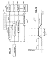
- the microdeposition head 50 includes a plurality of nozzles 230 that are preferably spaced uniformly. However, non-uniform spacing can also be used.
- the angular orientation of the microdeposition head 50 is adjusted relative to a plane defined by lateral movement of the head assembly and/or the substrate.
- the pitch is at a maximum value as is illustrated at 330.
- an area that is swept by the head 50 is also at a maximum value as indicated at 332.
- the pitch decreases as indicated at 340.
- the area that is swept by the head 50 also decreases as indicated at 342.
- over-clocking generally illustrated at 350 is used to provide improved resolution and to optionally adjust for changes in the pitch of the head 50.
- over-clocking refers to an increased clock frequency relative to a droplet width and a lateral and vertical speed of the head.
- a print grid is defined that includes grid lines that occur at a clock rate.
- the clock rate and lateral and vertical head speed are synchronized to provide (or not provide) one droplet in each rectangle (or square) of the grid.
- the droplet to grid rectangle ratio is 1:1.
- Some minor overlapping of droplets may occur in ink jets. Either a droplet is produced or is not produced in each rectangle or square of the grid.
- Over-clocking involves using a clock rate that is substantially higher.
- the clock rate is increased at least 3 times the conventional 1:1 ratio.
- the clock rate is increased 10x.
- a first nozzle 350-1 is fired at first and second times 354 and 355.
- a second nozzle 350-2 is fired at third and fourth times 356 and 357, which are later than the first and second times 354 and 355, respectively.
- a third nozzle 350-3 is fired at a fifth and sixth times 358 and 359, which are later than the second time 356.
- the dwell period between the time values for adjacent nozzles is determined by the pitch of the head 50. As the pitch decreases, the dwell period increases. Dotted lines at 360 show nozzle timing for smaller pitches.
- over-clocking also allows fluid material to be fired rapidly from the nozzles.
- a single nozzle is fired repeatedly at 362 and 364 during adjacent clock cycles.
- FIG. 34 shows overlapping droplets 366-1, 366-2, and 366-3 and 368-1, 368-2, and 368-3 that are fired from a single nozzle.
- the amount of overlap and the spacing is determined by the over-clocking rate and the speed that the substrate 53 and/or head assembly 24 is moved.
- uncorrected nozzle waveforms 370-1, 370-2, 370-3, ... and 370-8 that correspond to droplets 374-1, 374-2, 374-3, ..., and 374-8 are shown.
- the droplet 374-1 is slightly larger than desired.
- Droplet 374-2 is slightly larger and earlier than desired.
- Droplets 374-3, 374-7 and 374-8 are okay.
- Droplet 374-4 is smaller and later than desired.
- Droplet 374-5 is later than desired and needs improved droplet quality.
- corrected nozzle waveforms 380-1, 380-2, 380-3, ... and 380-8 that correspond to droplets 384-1, 384-2, 384-3, ..., and 384-8 are shown.
- the nozzle firing waveform 381 has an adjusted amplitude.
- the nozzle firing waveform 382 has an adjusted amplitude and start time.
- the nozzle firing waveform 383 is left unchanged.
- the nozzle firing waveform 384 has an adjusted amplitude and start time.
- the nozzle firing waveform 385 has an adjusted rise slope and start time.
- the nozzle firing waveform 386 has adjusted amplitude.
- the nozzle firing waveform 384-7 and 384-8 are unchanged.
- the corrected nozzle waveforms 380 have uniform or desired shape and correct timing.
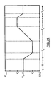
- over-clocking also allows improved resolution when defining features using microdeposition. For example, when depositing a diagonal feature line 390 without over-clocking, a jagged feature line 392 results because the droplets in the jagged feature line 392 must be aligned with a grid 394. When over-clocking is used in FIG. 37 , the droplets 396 is placed between the grid 394 and a more accurate feature line is produced.
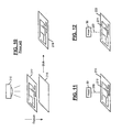
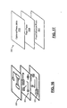
- a first modified microdeposition head 400 includes multiple microdeposition heads 402-1, 402-2, and 402-3 that are connected together or otherwise mounted in fixed relative positions. As can be appreciated, the modified microdeposition head 400 provides a reduced pitch as compared with a single microdeposition head 402.
- a second modified microdeposition head 420 is shown.
- the microdeposition head 420 includes multiple microdeposition heads 422-1, 422-2, and 422-3 that are moveable using actuators 424-1, 424-2, and 424-3 as indicated by arrows 426-1, 426-2, and 426-3.
- the angular position of the second modified microdeposition head 420 and the actuators 422 are adjusted by the controller 22 to provide a plurality of pitches.
Applications Claiming Priority (5)
| Application Number | Priority Date | Filing Date | Title |
|---|---|---|---|
| US29511801P | 2001-06-01 | 2001-06-01 | |
| US29510001P | 2001-06-01 | 2001-06-01 | |
| US295100P | 2001-06-01 | ||
| US295118P | 2001-06-01 | ||
| PCT/US2002/017375 WO2002098573A1 (en) | 2001-06-01 | 2002-05-31 | Waveform generator for microdeposition control system |
Publications (3)
| Publication Number | Publication Date |
|---|---|
| EP1399269A1 EP1399269A1 (en) | 2004-03-24 |
| EP1399269A4 EP1399269A4 (en) | 2005-08-24 |
| EP1399269B1 true EP1399269B1 (en) | 2010-11-03 |
Family
ID=26968921
Family Applications (7)
| Application Number | Title | Priority Date | Filing Date |
|---|---|---|---|
| EP02739641A Expired - Lifetime EP1399268B1 (en) | 2001-06-01 | 2002-05-31 | Industrial microdeposition system for polymer light emitting diode displays, printed circuit boards and the like |
| EP02752022A Withdrawn EP1569757A4 (en) | 2001-06-01 | 2002-05-31 | MICRO-POSITIONING APPARATUS FOR MULTIPLE LIQUID MATERIALS |
| EP02752023A Withdrawn EP1399951A4 (en) | 2001-06-01 | 2002-05-31 | DEVICE WITH INTERCHANGEABLE MICRO-BEARING HEAD AND METHOD |
| EP02739640A Expired - Lifetime EP1392449B1 (en) | 2001-06-01 | 2002-05-31 | Over-clocking in a microdeposition control system to improve resolution |
| EP02752021A Withdrawn EP1399950A4 (en) | 2001-06-01 | 2002-05-31 | FORMATION OF STRUCTURES ON A CIRCUIT BOARD PRINTED USING A PIEZO MICRODEPOSITION |
| EP02756113A Expired - Lifetime EP1399269B1 (en) | 2001-06-01 | 2002-05-31 | Waveform generator for microdeposition control system |
| EP02739639A Expired - Lifetime EP1399267B1 (en) | 2001-06-01 | 2002-05-31 | Microdeposition apparatus |
Family Applications Before (5)
| Application Number | Title | Priority Date | Filing Date |
|---|---|---|---|
| EP02739641A Expired - Lifetime EP1399268B1 (en) | 2001-06-01 | 2002-05-31 | Industrial microdeposition system for polymer light emitting diode displays, printed circuit boards and the like |
| EP02752022A Withdrawn EP1569757A4 (en) | 2001-06-01 | 2002-05-31 | MICRO-POSITIONING APPARATUS FOR MULTIPLE LIQUID MATERIALS |
| EP02752023A Withdrawn EP1399951A4 (en) | 2001-06-01 | 2002-05-31 | DEVICE WITH INTERCHANGEABLE MICRO-BEARING HEAD AND METHOD |
| EP02739640A Expired - Lifetime EP1392449B1 (en) | 2001-06-01 | 2002-05-31 | Over-clocking in a microdeposition control system to improve resolution |
| EP02752021A Withdrawn EP1399950A4 (en) | 2001-06-01 | 2002-05-31 | FORMATION OF STRUCTURES ON A CIRCUIT BOARD PRINTED USING A PIEZO MICRODEPOSITION |
Family Applications After (1)
| Application Number | Title | Priority Date | Filing Date |
|---|---|---|---|
| EP02739639A Expired - Lifetime EP1399267B1 (en) | 2001-06-01 | 2002-05-31 | Microdeposition apparatus |
Country Status (9)
| Country | Link |
|---|---|
| US (1) | US7270712B2 (zh) |
| EP (7) | EP1399268B1 (zh) |
| JP (9) | JP4342302B2 (zh) |
| KR (8) | KR100882520B1 (zh) |
| CN (7) | CN1329130C (zh) |
| AT (3) | ATE458555T1 (zh) |
| AU (4) | AU2002346740A1 (zh) |
| DE (3) | DE60238190D1 (zh) |
| WO (8) | WO2002098576A1 (zh) |
Cited By (1)
| Publication number | Priority date | Publication date | Assignee | Title |
|---|---|---|---|---|
| CN102862402A (zh) * | 2012-10-17 | 2013-01-09 | 东莞凯佳智芯电子科技有限公司 | 一种阵列式精密喷印设备的喷印控制方法与系统 |
Families Citing this family (98)
| Publication number | Priority date | Publication date | Assignee | Title |
|---|---|---|---|---|
| JP4971560B2 (ja) * | 2001-08-06 | 2012-07-11 | キヤノン株式会社 | インクジェット記録装置、ヘッドユニット及びカラーフィルタ製造装置 |
| EP1548448A4 (en) * | 2002-09-27 | 2009-11-11 | Shimadzu Corp | FLUORITY SPORTS METHOD AND DEVICE |
| US7964237B2 (en) * | 2003-08-21 | 2011-06-21 | International Business Machines Corporation | Fully automated paste dispense process for dispensing small dots and lines |
| TWI220076B (en) * | 2003-08-27 | 2004-08-01 | Au Optronics Corp | Light-emitting device |
| KR101026935B1 (ko) | 2003-12-10 | 2011-04-04 | 엘지디스플레이 주식회사 | 디스펜서 정렬장치 및 그 방법 |
| JP4195366B2 (ja) * | 2003-12-19 | 2008-12-10 | シャープ株式会社 | 薬液塗布方法および薬液塗布装置 |
| WO2005078533A1 (en) * | 2004-02-10 | 2005-08-25 | Zebra Imaging, Inc. | Deposition of photosensitive media for digital hologram recording |
| US7354845B2 (en) | 2004-08-24 | 2008-04-08 | Otb Group B.V. | In-line process for making thin film electronic devices |
| NL1026013C2 (nl) | 2004-04-23 | 2005-10-25 | Otb Group Bv | Werkwijze en inrichting voor het nauwkeurig aanbrengen van structuren op een substraat. |
| TWI547431B (zh) | 2004-06-09 | 2016-09-01 | 史密斯克萊美占公司 | 生產藥物之裝置及方法 |
| US8101244B2 (en) * | 2004-06-09 | 2012-01-24 | Smithkline Beecham Corporation | Apparatus and method for producing or processing a product or sample |
| US20060092218A1 (en) * | 2004-11-04 | 2006-05-04 | Applied Materials, Inc. | Methods and apparatus for inkjet printing |
| JP2006137124A (ja) * | 2004-11-15 | 2006-06-01 | Konica Minolta Holdings Inc | 液体吐出装置及び液体吐出方法 |
| WO2006064792A1 (ja) * | 2004-12-14 | 2006-06-22 | Ulvac, Inc. | 塗布装置、有機材料薄膜の形成方法、有機elパネル製造装置 |
| JP2006175727A (ja) * | 2004-12-22 | 2006-07-06 | Konica Minolta Holdings Inc | 液滴吐出制御装置 |
| EP1836056B1 (en) * | 2004-12-30 | 2018-11-07 | Fujifilm Dimatix, Inc. | Ink jet printing |
| US7824466B2 (en) | 2005-01-14 | 2010-11-02 | Cabot Corporation | Production of metal nanoparticles |
| US20060189113A1 (en) | 2005-01-14 | 2006-08-24 | Cabot Corporation | Metal nanoparticle compositions |
| WO2006076606A2 (en) | 2005-01-14 | 2006-07-20 | Cabot Corporation | Optimized multi-layer printing of electronics and displays |
| US8167393B2 (en) | 2005-01-14 | 2012-05-01 | Cabot Corporation | Printable electronic features on non-uniform substrate and processes for making same |
| WO2006076605A2 (en) * | 2005-01-14 | 2006-07-20 | Cabot Corporation | Circuit modeling and selective deposition |
| WO2006076607A1 (en) * | 2005-01-14 | 2006-07-20 | Cabot Corporation | Ink-jet printing of passive electricalcomponents |
| US20060160373A1 (en) * | 2005-01-14 | 2006-07-20 | Cabot Corporation | Processes for planarizing substrates and encapsulating printable electronic features |
| US8383014B2 (en) | 2010-06-15 | 2013-02-26 | Cabot Corporation | Metal nanoparticle compositions |
| US7533361B2 (en) * | 2005-01-14 | 2009-05-12 | Cabot Corporation | System and process for manufacturing custom electronics by combining traditional electronics with printable electronics |
| JP2006195863A (ja) * | 2005-01-17 | 2006-07-27 | Fujitsu Ten Ltd | エラー検出装置 |
| US20060163563A1 (en) * | 2005-01-24 | 2006-07-27 | Kurt Ulmer | Method to form a thin film resistor |
| WO2007004627A1 (ja) * | 2005-07-05 | 2007-01-11 | Konica Minolta Holdings, Inc. | パターニング装置、有機エレクトロルミネッセンス素子とその製造方法及び有機エレクトロルミネッセンス表示装置 |
| JP5509509B2 (ja) * | 2005-09-30 | 2014-06-04 | コニカミノルタ株式会社 | 液滴吐出装置、液滴速度調整方法、液滴速度検出装置、液滴速度検出方法、プログラム及び記録媒体 |
| CN101282842B (zh) * | 2005-10-07 | 2010-09-01 | 皇家飞利浦电子股份有限公司 | 用于将物质小滴受控地定位到基底上的喷墨装置和方法 |
| TWI287828B (en) | 2005-12-30 | 2007-10-01 | Ind Tech Res Inst | Method for printing a pattern and data processing method thereof |
| JP4058453B2 (ja) * | 2006-05-08 | 2008-03-12 | シャープ株式会社 | 液滴塗布装置 |
| TWI318176B (en) | 2006-11-08 | 2009-12-11 | Ind Tech Res Inst | Printing method |
| TWI320754B (en) | 2006-11-10 | 2010-02-21 | Ind Tech Res Inst | A print data processing mothod and device therefor |
| US7988247B2 (en) | 2007-01-11 | 2011-08-02 | Fujifilm Dimatix, Inc. | Ejection of drops having variable drop size from an ink jet printer |
| JP2008201018A (ja) * | 2007-02-21 | 2008-09-04 | Toppan Printing Co Ltd | インクジェットヘッドのアライメント装置 |
| JP5391524B2 (ja) * | 2007-03-23 | 2014-01-15 | 凸版印刷株式会社 | インクジェットヘッド管理装置 |
| US8186790B2 (en) * | 2008-03-14 | 2012-05-29 | Purdue Research Foundation | Method for producing ultra-small drops |
| DE102008057005A1 (de) * | 2008-11-11 | 2010-05-12 | Jonas & Redmann Automationstechnik Gmbh | Verfahren zum Positionieren und/oder Führen mindestens eines beliebigen Prozesskopfes für die Metallisierung von dünnen Substraten in einem definierten Abstand über der Substratoberfläche |
| CN101462414B (zh) * | 2008-11-28 | 2011-03-23 | 江苏康众数字医疗设备有限公司 | 用于电子元件集成的印刷装置及印刷方法 |
| ATE550170T1 (de) | 2008-12-19 | 2012-04-15 | Agfa Graphics Nv | Bildverarbeitungsverfahren für dreidimensionales drucken |
| US20100156768A1 (en) * | 2008-12-22 | 2010-06-24 | Fletcher Ii James Douglas | Display media, method of forming display media, and printer for printing on display media |
| JP5401163B2 (ja) * | 2009-04-30 | 2014-01-29 | パナソニック株式会社 | インクジェット印刷装置 |
| US20100300355A1 (en) * | 2009-06-01 | 2010-12-02 | Moser Baer India Limited | Printing material profiles onto substrates |
| US20130099666A1 (en) * | 2011-10-21 | 2013-04-25 | Almax Rp Corp. | Selectively controlling the resistance of resistive traces printed on a substrate to supply equal current to an array of light sources |
| JP6057406B2 (ja) * | 2012-01-06 | 2017-01-11 | 住友重機械工業株式会社 | 薄膜形成装置及び薄膜形成方法 |
| FR2990055B1 (fr) * | 2012-04-30 | 2014-12-26 | Total Sa | Matrice de depot d'au moins un fluide conducteur sur un substrat, ainsi que dispositif comprenant cette matrice et procede de depot |
| JP5750414B2 (ja) * | 2012-08-27 | 2015-07-22 | 東芝テック株式会社 | インクジェットヘッド駆動装置 |
| US11141752B2 (en) | 2012-12-27 | 2021-10-12 | Kateeva, Inc. | Techniques for arrayed printing of a permanent layer with improved speed and accuracy |
| US9700908B2 (en) | 2012-12-27 | 2017-07-11 | Kateeva, Inc. | Techniques for arrayed printing of a permanent layer with improved speed and accuracy |
| CN105073434B (zh) | 2012-12-27 | 2017-12-26 | 科迪华公司 | 用于打印油墨体积控制以在精确公差内沉积流体的方法和系统 |
| US11673155B2 (en) | 2012-12-27 | 2023-06-13 | Kateeva, Inc. | Techniques for arrayed printing of a permanent layer with improved speed and accuracy |
| US9832428B2 (en) | 2012-12-27 | 2017-11-28 | Kateeva, Inc. | Fast measurement of droplet parameters in industrial printing system |
| US9352561B2 (en) | 2012-12-27 | 2016-05-31 | Kateeva, Inc. | Techniques for print ink droplet measurement and control to deposit fluids within precise tolerances |
| WO2014193961A1 (en) * | 2013-05-31 | 2014-12-04 | Johnson Controls Technology Company | System and method for forming a vehicle trim component via additive manufacturing, and vehicle trim component |
| CN107825886B (zh) | 2013-12-12 | 2020-04-14 | 科迪华公司 | 制造电子设备的方法 |
| US20150197062A1 (en) * | 2014-01-12 | 2015-07-16 | Zohar SHINAR | Method, device, and system of three-dimensional printing |
| EP2902206B1 (en) * | 2014-01-31 | 2021-06-09 | HP Scitex Ltd | Printhead arrangement on a printbar beam member |
| US10391705B2 (en) * | 2014-05-09 | 2019-08-27 | Nike, Inc. | System and method for forming three-dimensional structures |
| US9387671B2 (en) | 2014-05-14 | 2016-07-12 | Ricoh Company, Ltd. | Head driving device, recording head unit, and image forming apparatus |
| US9147875B1 (en) | 2014-09-10 | 2015-09-29 | Cellink Corporation | Interconnect for battery packs |
| US10211443B2 (en) | 2014-09-10 | 2019-02-19 | Cellink Corporation | Battery interconnects |
| CN104385592B (zh) * | 2014-10-14 | 2016-12-07 | 秦皇岛天秦三维数字化技术有限公司 | 3d打印机机电控制系统及方法 |
| JP6296960B2 (ja) * | 2014-10-31 | 2018-03-20 | 株式会社東芝 | インクジェットヘッド、及び、印刷装置 |
| CN105643921B (zh) * | 2014-11-11 | 2018-09-25 | 三纬国际立体列印科技股份有限公司 | 立体打印装置与立体打印方法 |
| CN107408544B (zh) * | 2015-02-03 | 2019-09-13 | 塞林克公司 | 用于组合式热能与电能传递的系统及方法 |
| US10029425B2 (en) * | 2015-04-07 | 2018-07-24 | Sartorius Stedim Biotech Gmbh | Container for accommodating at least one of at least one biologically active fluid and at least one preparatory fluid, and a method therefor |
| JP6479555B2 (ja) * | 2015-04-27 | 2019-03-06 | 住友重機械工業株式会社 | 膜形成装置 |
| WO2017108071A1 (de) | 2015-12-21 | 2017-06-29 | Wacker Chemie Ag | Verfahren und vorrichtung zur herstellung eines objekts unter einsatz einer 3d-druckvorrichtung |
| JP6387955B2 (ja) * | 2015-12-25 | 2018-09-12 | セイコーエプソン株式会社 | ヘッドユニット制御回路 |
| EP3490801B1 (en) * | 2016-07-27 | 2021-06-30 | President and Fellows of Harvard College | Apparatus and method for acoustophoretic printing |
| CN107952958B (zh) * | 2016-10-16 | 2020-01-10 | 北京煜鼎增材制造研究院有限公司 | 沉积轴、增材制造设备及对沉积轴行程进行调节的方法 |
| DE102016014948A1 (de) | 2016-12-14 | 2018-06-14 | Dürr Systems Ag | Druckkopf und zugehöriges Betriebsverfahren |
| DE102016014946A1 (de) | 2016-12-14 | 2018-06-14 | Dürr Systems Ag | Druckkopf zur Applikation eines Beschichtungsmittels auf ein Bauteil |
| DE102016014943A1 (de) | 2016-12-14 | 2018-06-14 | Dürr Systems Ag | Druckkopf mit Temperiereinrichtung |
| DE102016014955A1 (de) | 2016-12-14 | 2018-06-14 | Dürr Systems Ag | Beschichtungseinrichtung und entsprechendes Beschichtungsverfahren |
| DE102016014944A1 (de) | 2016-12-14 | 2018-06-14 | Dürr Systems Ag | Beschichtungsverfahren und entsprechende Beschichtungseinrichtung |
| DE102016014953A1 (de) | 2016-12-14 | 2018-06-14 | Dürr Systems Ag | Lackieranlage und entsprechendes Lackierverfahren |
| DE102016014952A1 (de) | 2016-12-14 | 2018-06-14 | Dürr Systems Ag | Beschichtungseinrichtung zur Beschichtung von Bauteilen |
| DE102016014919A1 (de) | 2016-12-14 | 2018-06-14 | Dürr Systems Ag | Applikationsvorrichtung und Verfahren zum Applizieren eines Beschichtungsmittels |
| DE102016014951A1 (de) | 2016-12-14 | 2018-06-14 | Dürr Systems Ag | Beschichtungseinrichtung und zugehöriges Betriebsverfahren |
| DE102016014956A1 (de) | 2016-12-14 | 2018-06-14 | Dürr Systems Ag | Beschichtungseinrichtung und zugehöriges Betriebsverfahren |
| DE102016014920A1 (de) * | 2016-12-14 | 2018-06-14 | Dürr Systems Ag | Druckkopf mit Verschiebe- und/oder Drehmechanik für zumindest eine Düsenreihe |
| DE102016014947A1 (de) | 2016-12-14 | 2018-06-14 | Dürr Systems Ag | Druckkopf zur Applikation eines Beschichtungsmittels |
| JP6999317B2 (ja) * | 2017-07-21 | 2022-01-18 | 東芝テック株式会社 | インクジェットヘッド及びインクジェットプリンタ |
| EP3700680A1 (en) | 2017-10-27 | 2020-09-02 | Nordson Corporation | Systems and methods for closed loop fluid velocity control for jetting |
| US20190217327A1 (en) * | 2018-01-15 | 2019-07-18 | Tokyo Electron Limited | System and Method for Fluid Dispense and Coverage Control |
| FR3080998B1 (fr) * | 2018-05-14 | 2020-04-24 | Reydel Automotive B.V. | Procede de traitement de surface d'une piece et installation associee |
| EP3588099A1 (en) * | 2018-06-26 | 2020-01-01 | Tecan Trading Ag | Positioning assembly for a laboratory apparatus |
| CN110271288B (zh) * | 2019-07-05 | 2020-05-22 | 深圳市华星光电半导体显示技术有限公司 | Oled喷墨打印喷头及其打印装置 |
| CN110424032A (zh) * | 2019-09-10 | 2019-11-08 | 江苏师范大学 | 一种用于压力机主轴修复的射流电沉积装置及其方法 |
| CN111231316A (zh) * | 2020-03-02 | 2020-06-05 | 爱司达智能制造(江苏)有限公司 | 一种增材设备的流道结构 |
| CN111286699B (zh) * | 2020-03-25 | 2022-04-05 | 中国工程物理研究院激光聚变研究中心 | 一种挡板修正方法、镀膜方法和装置 |
| CN111653184B (zh) * | 2020-07-10 | 2022-05-10 | 宿迁市规划测绘院有限公司 | 一种拥有多功能放置台的3d地图批量喷绘控制系统 |
| EP4256647A1 (en) | 2021-03-24 | 2023-10-11 | CelLink Corporation | Multilayered flexible battery interconnects and methods of fabricating thereof |
| CN113245102B (zh) * | 2021-06-07 | 2022-02-25 | 苏州微知电子科技有限公司 | 一种纤维器件喷涂机 |
| CN114161707A (zh) * | 2021-12-10 | 2022-03-11 | 苏州华星光电技术有限公司 | 打印设备及打印方法 |
| CN114474718A (zh) * | 2021-12-28 | 2022-05-13 | 郭超 | 一种3d打印检测方法、装置、设备及3d打印系统 |
Family Cites Families (58)
| Publication number | Priority date | Publication date | Assignee | Title |
|---|---|---|---|---|
| US3572400A (en) * | 1967-08-31 | 1971-03-23 | Western Electric Co | Dispensing of fluids to small areas |
| US4037830A (en) * | 1976-09-07 | 1977-07-26 | International Business Machines Corporation | Wafer handler |
| JPS5590806A (en) * | 1978-12-29 | 1980-07-09 | Ricoh Co Ltd | Apparatus for measuring diameter of ink jet particle |
| US4795518A (en) * | 1984-02-17 | 1989-01-03 | Burr-Brown Corporation | Method using a multiple device vacuum chuck for an automatic microelectronic bonding apparatus |
| US4575330A (en) * | 1984-08-08 | 1986-03-11 | Uvp, Inc. | Apparatus for production of three-dimensional objects by stereolithography |
| US4835704A (en) * | 1986-12-29 | 1989-05-30 | General Electric Company | Adaptive lithography system to provide high density interconnect |
| US5002008A (en) * | 1988-05-27 | 1991-03-26 | Tokyo Electron Limited | Coating apparatus and method for applying a liquid to a semiconductor wafer, including selecting a nozzle in a stand-by state |
| US5229016A (en) * | 1991-08-08 | 1993-07-20 | Microfab Technologies, Inc. | Method and apparatus for dispensing spherical-shaped quantities of liquid solder |
| JPH05149769A (ja) * | 1991-11-29 | 1993-06-15 | Canon Inc | インクジエツト記録ヘツドのインク噴射体積測定方法および測定装置 |
| US5320250A (en) * | 1991-12-02 | 1994-06-14 | Asymptotic Technologies, Inc. | Method for rapid dispensing of minute quantities of viscous material |
| US5738165A (en) * | 1993-05-07 | 1998-04-14 | Nikon Corporation | Substrate holding apparatus |
| US5736195A (en) * | 1993-09-15 | 1998-04-07 | Mobium Enterprises Corporation | Method of coating a thin film on a substrate |
| US5403617A (en) * | 1993-09-15 | 1995-04-04 | Mobium Enterprises Corporation | Hybrid pulsed valve for thin film coating and method |
| JPH07101062A (ja) * | 1993-09-30 | 1995-04-18 | Canon Inc | インクジェット記録装置及びその記録方法 |
| US5498444A (en) * | 1994-02-28 | 1996-03-12 | Microfab Technologies, Inc. | Method for producing micro-optical components |
| JPH07323550A (ja) * | 1994-05-31 | 1995-12-12 | Canon Inc | インクジェットプリント装置の制御方法およびインクジェットプリント装置 |
| JP3241251B2 (ja) * | 1994-12-16 | 2001-12-25 | キヤノン株式会社 | 電子放出素子の製造方法及び電子源基板の製造方法 |
| US5920331A (en) * | 1995-04-12 | 1999-07-06 | Eastman Kodak Company | Method and apparatus for accurate control of temperature pulses in printing heads |
| JPH091797A (ja) * | 1995-06-15 | 1997-01-07 | Toyo Electric Mfg Co Ltd | インクの着弾位置制御方法 |
| US5932012A (en) * | 1995-06-23 | 1999-08-03 | Hitachi Techno Engineering Co., Ltd. | Paste applicator having positioning means |
| CA2489818C (en) * | 1995-10-13 | 2007-07-24 | Nordson Corporation | A system for dispensing a viscous material onto a substrate |
| JP3627078B2 (ja) * | 1995-12-22 | 2005-03-09 | 富士写真フイルム株式会社 | インクジェット装置 |
| US5906683A (en) * | 1996-04-16 | 1999-05-25 | Applied Materials, Inc. | Lid assembly for semiconductor processing chamber |
| US5681757A (en) * | 1996-04-29 | 1997-10-28 | Microfab Technologies, Inc. | Process for dispensing semiconductor die-bond adhesive using a printhead having a microjet array and the product produced by the process |
| US5779971A (en) * | 1996-06-07 | 1998-07-14 | Hewlett-Packard Company | Solder jet printhead |
| JP3349891B2 (ja) * | 1996-06-11 | 2002-11-25 | 富士通株式会社 | 圧電型インクジェットヘッドの駆動方法 |
| JPH1050769A (ja) * | 1996-07-30 | 1998-02-20 | Toshiba Corp | 半導体パッケージの製造装置および製造方法 |
| US5756157A (en) * | 1996-10-02 | 1998-05-26 | Silicon Valley Group | Method for processing flat panel displays and large wafers |
| US6132809A (en) * | 1997-01-16 | 2000-10-17 | Precision Valve & Automation, Inc. | Conformal coating using multiple applications |
| US6224180B1 (en) * | 1997-02-21 | 2001-05-01 | Gerald Pham-Van-Diep | High speed jet soldering system |
| JPH10260307A (ja) * | 1997-03-17 | 1998-09-29 | Seiko Epson Corp | カラーフィルタの製造装置およびその方法 |
| JPH10284360A (ja) * | 1997-04-02 | 1998-10-23 | Hitachi Ltd | 基板温度制御装置及び方法 |
| SG135904A1 (en) * | 1997-07-04 | 2007-10-29 | Tokyo Electron Ltd | Process solution supplying apparatus |
| JP3695150B2 (ja) * | 1997-07-08 | 2005-09-14 | セイコーエプソン株式会社 | インクジェット記録装置及びその駆動波形制御方法 |
| US6193346B1 (en) * | 1997-07-22 | 2001-02-27 | Ricoh Company, Ltd. | Ink-jet recording apparatus |
| JPH1158735A (ja) * | 1997-08-18 | 1999-03-02 | Nec Niigata Ltd | インクジェット記録装置 |
| JPH11138820A (ja) * | 1997-09-05 | 1999-05-25 | Ricoh Co Ltd | 液滴の噴射特性測定方法およびシステム |
| JPH1177991A (ja) * | 1997-09-12 | 1999-03-23 | Seiko Epson Corp | インクジェット記録装置 |
| WO1999019900A2 (en) * | 1997-10-14 | 1999-04-22 | Patterning Technologies Limited | Method of forming an electronic device |
| US6007631A (en) * | 1997-11-10 | 1999-12-28 | Speedline Technologies, Inc. | Multiple head dispensing system and method |
| JPH11157055A (ja) * | 1997-11-28 | 1999-06-15 | Sony Corp | インクジェットプリンタ、ならびにインクジェットプリンタ用記録ヘッドの駆動装置および方法 |
| US6019164A (en) * | 1997-12-31 | 2000-02-01 | Temptronic Corporation | Workpiece chuck |
| GB9808182D0 (en) * | 1998-04-17 | 1998-06-17 | The Technology Partnership Plc | Liquid projection apparatus |
| JP3381776B2 (ja) * | 1998-05-19 | 2003-03-04 | 東京エレクトロン株式会社 | 処理装置および処理方法 |
| JP3611177B2 (ja) * | 1998-07-22 | 2005-01-19 | セイコーエプソン株式会社 | インクジェット式記録装置及び記録方法 |
| US6129872A (en) * | 1998-08-29 | 2000-10-10 | Jang; Justin | Process and apparatus for creating a colorful three-dimensional object |
| JP2000071437A (ja) * | 1998-09-02 | 2000-03-07 | Ricoh Co Ltd | インクジェット記録装置及び記憶媒体並びに制御テーブル作成方法 |
| US6190727B1 (en) * | 1998-10-30 | 2001-02-20 | Georgia-Pacific Corporation | Liquid coating spray applicator and method providing automatic spread rate control |
| JP4468500B2 (ja) * | 1998-11-16 | 2010-05-26 | ブラザー工業株式会社 | 移動物体の検出方法及びその装置 |
| US6318828B1 (en) * | 1999-02-19 | 2001-11-20 | Hewlett-Packard Company | System and method for controlling firing operations of an inkjet printhead |
| US6209964B1 (en) * | 1999-03-03 | 2001-04-03 | Jose Pinto | Dump truck vibrator |
| JP4208332B2 (ja) * | 1999-03-19 | 2009-01-14 | キヤノン株式会社 | インクジェットヘッドユニットの調整装置及び調整方法及びカラーフィルタの製造方法及び液晶表示パネルの製造方法 |
| GB2350321A (en) * | 1999-05-27 | 2000-11-29 | Patterning Technologies Ltd | Method of forming a masking or spacer pattern on a substrate using inkjet droplet deposition |
| CA2375365A1 (en) * | 1999-05-27 | 2001-02-15 | Patterning Technologies Limited | Method of forming a masking pattern on a surface |
| EP2374620A1 (en) * | 1999-09-30 | 2011-10-12 | Seiko Epson Corporation | Liquid jetting apparatus |
| JP3446686B2 (ja) * | 1999-10-21 | 2003-09-16 | セイコーエプソン株式会社 | インクジェット式記録装置 |
| US6420202B1 (en) * | 2000-05-16 | 2002-07-16 | Agere Systems Guardian Corp. | Method for shaping thin film resonators to shape acoustic modes therein |
| US6596239B2 (en) * | 2000-12-12 | 2003-07-22 | Edc Biosystems, Inc. | Acoustically mediated fluid transfer methods and uses thereof |
-
2002
- 2002-05-31 EP EP02739641A patent/EP1399268B1/en not_active Expired - Lifetime
- 2002-05-31 CN CNB028148223A patent/CN1329130C/zh not_active Expired - Fee Related
- 2002-05-31 AT AT02739640T patent/ATE458555T1/de not_active IP Right Cessation
- 2002-05-31 KR KR1020037015744A patent/KR100882520B1/ko active IP Right Grant
- 2002-05-31 AU AU2002346740A patent/AU2002346740A1/en not_active Abandoned
- 2002-05-31 JP JP2003501606A patent/JP4342302B2/ja not_active Expired - Fee Related
- 2002-05-31 KR KR1020097020246A patent/KR100998171B1/ko active IP Right Grant
- 2002-05-31 WO PCT/US2002/017523 patent/WO2002098576A1/en active Application Filing
- 2002-05-31 WO PCT/US2002/017370 patent/WO2002099849A2/en not_active Application Discontinuation
- 2002-05-31 DE DE60238190T patent/DE60238190D1/de not_active Expired - Lifetime
- 2002-05-31 WO PCT/US2002/017522 patent/WO2002099851A2/en not_active Application Discontinuation
- 2002-05-31 WO PCT/US2002/017375 patent/WO2002098573A1/en active Application Filing
- 2002-05-31 AT AT02739639T patent/ATE486662T1/de not_active IP Right Cessation
- 2002-05-31 WO PCT/US2002/017519 patent/WO2002098574A1/en active Application Filing
- 2002-05-31 JP JP2003501607A patent/JP4342303B2/ja not_active Expired - Fee Related
- 2002-05-31 CN CNB028111400A patent/CN1285420C/zh not_active Expired - Fee Related
- 2002-05-31 AU AU2002346738A patent/AU2002346738A1/en not_active Abandoned
- 2002-05-31 US US10/479,318 patent/US7270712B2/en not_active Expired - Lifetime
- 2002-05-31 EP EP02752022A patent/EP1569757A4/en not_active Withdrawn
- 2002-05-31 DE DE60238189T patent/DE60238189D1/de not_active Expired - Lifetime
- 2002-05-31 WO PCT/US2002/017369 patent/WO2002099848A2/en not_active Application Discontinuation
- 2002-05-31 EP EP02752023A patent/EP1399951A4/en not_active Withdrawn
- 2002-05-31 AU AU2002346735A patent/AU2002346735A1/en not_active Abandoned
- 2002-05-31 CN CNB028111397A patent/CN1289207C/zh not_active Expired - Fee Related
- 2002-05-31 JP JP2003501604A patent/JP4342301B2/ja not_active Expired - Fee Related
- 2002-05-31 WO PCT/US2002/017373 patent/WO2002099850A2/en active Application Filing
- 2002-05-31 CN CNA028133021A patent/CN1635949A/zh active Pending
- 2002-05-31 EP EP02739640A patent/EP1392449B1/en not_active Expired - Lifetime
- 2002-05-31 AT AT02756113T patent/ATE486663T1/de not_active IP Right Cessation
- 2002-05-31 JP JP2003501605A patent/JP4328614B2/ja not_active Expired - Fee Related
- 2002-05-31 JP JP2003502865A patent/JP2004528978A/ja active Pending
- 2002-05-31 WO PCT/US2002/017521 patent/WO2002098575A1/en active Application Filing
- 2002-05-31 EP EP02752021A patent/EP1399950A4/en not_active Withdrawn
- 2002-05-31 JP JP2003502864A patent/JP2005515052A/ja active Pending
- 2002-05-31 DE DE60235458T patent/DE60235458D1/de not_active Expired - Lifetime
- 2002-05-31 KR KR10-2003-7015754A patent/KR20040038915A/ko not_active Application Discontinuation
- 2002-05-31 EP EP02756113A patent/EP1399269B1/en not_active Expired - Lifetime
- 2002-05-31 AU AU2002314894A patent/AU2002314894A1/en not_active Abandoned
- 2002-05-31 CN CNA028133110A patent/CN1630939A/zh active Pending
- 2002-05-31 KR KR1020037015750A patent/KR100938810B1/ko active IP Right Grant
- 2002-05-31 EP EP02739639A patent/EP1399267B1/en not_active Expired - Lifetime
- 2002-05-31 CN CNB028148231A patent/CN1280025C/zh not_active Expired - Fee Related
- 2002-05-31 KR KR10-2003-7015748A patent/KR20040026659A/ko not_active Application Discontinuation
- 2002-05-31 CN CNB028111206A patent/CN1274425C/zh not_active Expired - Fee Related
- 2002-05-31 KR KR10-2003-7015752A patent/KR20040024558A/ko not_active Application Discontinuation
- 2002-05-31 KR KR1020037015742A patent/KR100924002B1/ko active IP Right Grant
- 2002-05-31 KR KR1020037015746A patent/KR100912008B1/ko active IP Right Grant
- 2002-05-31 JP JP2003502863A patent/JP2004533121A/ja active Pending
-
2009
- 2009-01-26 JP JP2009014785A patent/JP5145259B2/ja not_active Expired - Lifetime
- 2009-01-26 JP JP2009014781A patent/JP4880708B2/ja not_active Expired - Fee Related
Cited By (2)
| Publication number | Priority date | Publication date | Assignee | Title |
|---|---|---|---|---|
| CN102862402A (zh) * | 2012-10-17 | 2013-01-09 | 东莞凯佳智芯电子科技有限公司 | 一种阵列式精密喷印设备的喷印控制方法与系统 |
| CN102862402B (zh) * | 2012-10-17 | 2015-07-22 | 佛山市智巢电子科技有限公司 | 一种阵列式精密喷印设备的喷印控制方法与系统 |
Also Published As
Similar Documents
| Publication | Publication Date | Title |
|---|---|---|
| EP1399269B1 (en) | Waveform generator for microdeposition control system | |
| US7757632B2 (en) | Waveform generator for microdeposition control system | |
| US7815965B2 (en) | Industrial microdeposition system including masking to reduce the impact of droplet alignment and droplet volume tolerances and errors | |
| US7244310B2 (en) | Over-clocking in a microdeposition control system to improve resolution | |
| KR100942425B1 (ko) | 유체방울의 정렬 및 그 체적공차 및 오류로 인한 악영향을 감소시키기 위한 마스킹을 갖춘 산업용 미세적층장치 및 그 방법 |
Legal Events
| Date | Code | Title | Description |
|---|---|---|---|
| PUAI | Public reference made under article 153(3) epc to a published international application that has entered the european phase |
Free format text: ORIGINAL CODE: 0009012 |
|
| 17P | Request for examination filed |
Effective date: 20031206 |
|
| AK | Designated contracting states |
Kind code of ref document: A1 Designated state(s): AT BE CH CY DE DK ES FI FR GB GR IE IT LI LU MC NL PT SE TR |
|
| AX | Request for extension of the european patent |
Extension state: AL LT LV MK RO SI |
|
| RAP1 | Party data changed (applicant data changed or rights of an application transferred) |
Owner name: LITREX CORPORATION |
|
| A4 | Supplementary search report drawn up and despatched |
Effective date: 20050708 |
|
| RIC1 | Information provided on ipc code assigned before grant |
Ipc: 7B 41J 2/05 B Ipc: 7B 05C 11/10 A Ipc: 7B 41J 2/045 B |
|
| RAP1 | Party data changed (applicant data changed or rights of an application transferred) |
Owner name: ULVAC, INC. |
|
| 17Q | First examination report despatched |
Effective date: 20090630 |
|
| GRAP | Despatch of communication of intention to grant a patent |
Free format text: ORIGINAL CODE: EPIDOSNIGR1 |
|
| GRAS | Grant fee paid |
Free format text: ORIGINAL CODE: EPIDOSNIGR3 |
|
| GRAA | (expected) grant |
Free format text: ORIGINAL CODE: 0009210 |
|
| AK | Designated contracting states |
Kind code of ref document: B1 Designated state(s): AT BE CH CY DE DK ES FI FR GB GR IE IT LI LU MC NL PT SE TR |
|
| REG | Reference to a national code |
Ref country code: GB Ref legal event code: FG4D |
|
| REG | Reference to a national code |
Ref country code: CH Ref legal event code: EP |
|
| REG | Reference to a national code |
Ref country code: IE Ref legal event code: FG4D |
|
| REF | Corresponds to: |
Ref document number: 60238190 Country of ref document: DE Date of ref document: 20101216 Kind code of ref document: P |
|
| REG | Reference to a national code |
Ref country code: NL Ref legal event code: T3 |
|
| PG25 | Lapsed in a contracting state [announced via postgrant information from national office to epo] |
Ref country code: AT Free format text: LAPSE BECAUSE OF FAILURE TO SUBMIT A TRANSLATION OF THE DESCRIPTION OR TO PAY THE FEE WITHIN THE PRESCRIBED TIME-LIMIT Effective date: 20101103 Ref country code: PT Free format text: LAPSE BECAUSE OF FAILURE TO SUBMIT A TRANSLATION OF THE DESCRIPTION OR TO PAY THE FEE WITHIN THE PRESCRIBED TIME-LIMIT Effective date: 20110303 Ref country code: FI Free format text: LAPSE BECAUSE OF FAILURE TO SUBMIT A TRANSLATION OF THE DESCRIPTION OR TO PAY THE FEE WITHIN THE PRESCRIBED TIME-LIMIT Effective date: 20101103 Ref country code: SE Free format text: LAPSE BECAUSE OF FAILURE TO SUBMIT A TRANSLATION OF THE DESCRIPTION OR TO PAY THE FEE WITHIN THE PRESCRIBED TIME-LIMIT Effective date: 20101103 |
|
| PG25 | Lapsed in a contracting state [announced via postgrant information from national office to epo] |
Ref country code: GR Free format text: LAPSE BECAUSE OF FAILURE TO SUBMIT A TRANSLATION OF THE DESCRIPTION OR TO PAY THE FEE WITHIN THE PRESCRIBED TIME-LIMIT Effective date: 20110204 |
|
| PG25 | Lapsed in a contracting state [announced via postgrant information from national office to epo] |
Ref country code: ES Free format text: LAPSE BECAUSE OF FAILURE TO SUBMIT A TRANSLATION OF THE DESCRIPTION OR TO PAY THE FEE WITHIN THE PRESCRIBED TIME-LIMIT Effective date: 20110214 Ref country code: BE Free format text: LAPSE BECAUSE OF FAILURE TO SUBMIT A TRANSLATION OF THE DESCRIPTION OR TO PAY THE FEE WITHIN THE PRESCRIBED TIME-LIMIT Effective date: 20101103 |
|
| PG25 | Lapsed in a contracting state [announced via postgrant information from national office to epo] |
Ref country code: DK Free format text: LAPSE BECAUSE OF FAILURE TO SUBMIT A TRANSLATION OF THE DESCRIPTION OR TO PAY THE FEE WITHIN THE PRESCRIBED TIME-LIMIT Effective date: 20101103 |
|
| PLBE | No opposition filed within time limit |
Free format text: ORIGINAL CODE: 0009261 |
|
| STAA | Information on the status of an ep patent application or granted ep patent |
Free format text: STATUS: NO OPPOSITION FILED WITHIN TIME LIMIT |
|
| 26N | No opposition filed |
Effective date: 20110804 |
|
| REG | Reference to a national code |
Ref country code: DE Ref legal event code: R097 Ref document number: 60238190 Country of ref document: DE Effective date: 20110804 |
|
| PG25 | Lapsed in a contracting state [announced via postgrant information from national office to epo] |
Ref country code: IT Free format text: LAPSE BECAUSE OF FAILURE TO SUBMIT A TRANSLATION OF THE DESCRIPTION OR TO PAY THE FEE WITHIN THE PRESCRIBED TIME-LIMIT Effective date: 20101103 Ref country code: MC Free format text: LAPSE BECAUSE OF NON-PAYMENT OF DUE FEES Effective date: 20110531 |
|
| REG | Reference to a national code |
Ref country code: CH Ref legal event code: PL |
|
| PG25 | Lapsed in a contracting state [announced via postgrant information from national office to epo] |
Ref country code: LI Free format text: LAPSE BECAUSE OF NON-PAYMENT OF DUE FEES Effective date: 20110531 Ref country code: CH Free format text: LAPSE BECAUSE OF NON-PAYMENT OF DUE FEES Effective date: 20110531 |
|
| REG | Reference to a national code |
Ref country code: FR Ref legal event code: ST Effective date: 20120131 |
|
| REG | Reference to a national code |
Ref country code: IE Ref legal event code: MM4A |
|
| PG25 | Lapsed in a contracting state [announced via postgrant information from national office to epo] |
Ref country code: IE Free format text: LAPSE BECAUSE OF NON-PAYMENT OF DUE FEES Effective date: 20110531 Ref country code: FR Free format text: LAPSE BECAUSE OF NON-PAYMENT OF DUE FEES Effective date: 20110531 |
|
| PG25 | Lapsed in a contracting state [announced via postgrant information from national office to epo] |
Ref country code: LU Free format text: LAPSE BECAUSE OF NON-PAYMENT OF DUE FEES Effective date: 20110531 Ref country code: CY Free format text: LAPSE BECAUSE OF FAILURE TO SUBMIT A TRANSLATION OF THE DESCRIPTION OR TO PAY THE FEE WITHIN THE PRESCRIBED TIME-LIMIT Effective date: 20101103 |
|
| PG25 | Lapsed in a contracting state [announced via postgrant information from national office to epo] |
Ref country code: TR Free format text: LAPSE BECAUSE OF FAILURE TO SUBMIT A TRANSLATION OF THE DESCRIPTION OR TO PAY THE FEE WITHIN THE PRESCRIBED TIME-LIMIT Effective date: 20101103 |
|
| PGFP | Annual fee paid to national office [announced via postgrant information from national office to epo] |
Ref country code: DE Payment date: 20180529 Year of fee payment: 17 |
|
| PGFP | Annual fee paid to national office [announced via postgrant information from national office to epo] |
Ref country code: NL Payment date: 20180526 Year of fee payment: 17 |
|
| PGFP | Annual fee paid to national office [announced via postgrant information from national office to epo] |
Ref country code: GB Payment date: 20180529 Year of fee payment: 17 |
|
| REG | Reference to a national code |
Ref country code: DE Ref legal event code: R119 Ref document number: 60238190 Country of ref document: DE |
|
| REG | Reference to a national code |
Ref country code: NL Ref legal event code: MM Effective date: 20190601 |
|
| GBPC | Gb: european patent ceased through non-payment of renewal fee |
Effective date: 20190531 |
|
| PG25 | Lapsed in a contracting state [announced via postgrant information from national office to epo] |
Ref country code: DE Free format text: LAPSE BECAUSE OF NON-PAYMENT OF DUE FEES Effective date: 20191203 Ref country code: NL Free format text: LAPSE BECAUSE OF NON-PAYMENT OF DUE FEES Effective date: 20190601 Ref country code: GB Free format text: LAPSE BECAUSE OF NON-PAYMENT OF DUE FEES Effective date: 20190531 |