EP1398835A1 - Memoire magnetique et procede de commande associe, ainsi qu'appareil de memoire magnetique comprenant celle-ci - Google Patents
Memoire magnetique et procede de commande associe, ainsi qu'appareil de memoire magnetique comprenant celle-ci Download PDFInfo
- Publication number
- EP1398835A1 EP1398835A1 EP02736165A EP02736165A EP1398835A1 EP 1398835 A1 EP1398835 A1 EP 1398835A1 EP 02736165 A EP02736165 A EP 02736165A EP 02736165 A EP02736165 A EP 02736165A EP 1398835 A1 EP1398835 A1 EP 1398835A1
- Authority
- EP
- European Patent Office
- Prior art keywords
- memory
- layers
- current
- magnetic
- layer
- Prior art date
- Legal status (The legal status is an assumption and is not a legal conclusion. Google has not performed a legal analysis and makes no representation as to the accuracy of the status listed.)
- Withdrawn
Links
Images


Classifications
-
- H—ELECTRICITY
- H10—SEMICONDUCTOR DEVICES; ELECTRIC SOLID-STATE DEVICES NOT OTHERWISE PROVIDED FOR
- H10B—ELECTRONIC MEMORY DEVICES
- H10B61/00—Magnetic memory devices, e.g. magnetoresistive RAM [MRAM] devices
- H10B61/10—Magnetic memory devices, e.g. magnetoresistive RAM [MRAM] devices comprising components having two electrodes, e.g. diodes or MIM elements
-
- B—PERFORMING OPERATIONS; TRANSPORTING
- B82—NANOTECHNOLOGY
- B82Y—SPECIFIC USES OR APPLICATIONS OF NANOSTRUCTURES; MEASUREMENT OR ANALYSIS OF NANOSTRUCTURES; MANUFACTURE OR TREATMENT OF NANOSTRUCTURES
- B82Y10/00—Nanotechnology for information processing, storage or transmission, e.g. quantum computing or single electron logic
-
- G—PHYSICS
- G11—INFORMATION STORAGE
- G11C—STATIC STORES
- G11C11/00—Digital stores characterised by the use of particular electric or magnetic storage elements; Storage elements therefor
- G11C11/02—Digital stores characterised by the use of particular electric or magnetic storage elements; Storage elements therefor using magnetic elements
- G11C11/14—Digital stores characterised by the use of particular electric or magnetic storage elements; Storage elements therefor using magnetic elements using thin-film elements
- G11C11/15—Digital stores characterised by the use of particular electric or magnetic storage elements; Storage elements therefor using magnetic elements using thin-film elements using multiple magnetic layers
-
- G—PHYSICS
- G11—INFORMATION STORAGE
- G11C—STATIC STORES
- G11C11/00—Digital stores characterised by the use of particular electric or magnetic storage elements; Storage elements therefor
- G11C11/02—Digital stores characterised by the use of particular electric or magnetic storage elements; Storage elements therefor using magnetic elements
- G11C11/16—Digital stores characterised by the use of particular electric or magnetic storage elements; Storage elements therefor using magnetic elements using elements in which the storage effect is based on magnetic spin effect
- G11C11/161—Digital stores characterised by the use of particular electric or magnetic storage elements; Storage elements therefor using magnetic elements using elements in which the storage effect is based on magnetic spin effect details concerning the memory cell structure, e.g. the layers of the ferromagnetic memory cell
-
- G—PHYSICS
- G11—INFORMATION STORAGE
- G11C—STATIC STORES
- G11C11/00—Digital stores characterised by the use of particular electric or magnetic storage elements; Storage elements therefor
- G11C11/02—Digital stores characterised by the use of particular electric or magnetic storage elements; Storage elements therefor using magnetic elements
- G11C11/16—Digital stores characterised by the use of particular electric or magnetic storage elements; Storage elements therefor using magnetic elements using elements in which the storage effect is based on magnetic spin effect
- G11C11/165—Auxiliary circuits
- G11C11/1659—Cell access
-
- G—PHYSICS
- G11—INFORMATION STORAGE
- G11C—STATIC STORES
- G11C11/00—Digital stores characterised by the use of particular electric or magnetic storage elements; Storage elements therefor
- G11C11/02—Digital stores characterised by the use of particular electric or magnetic storage elements; Storage elements therefor using magnetic elements
- G11C11/16—Digital stores characterised by the use of particular electric or magnetic storage elements; Storage elements therefor using magnetic elements using elements in which the storage effect is based on magnetic spin effect
- G11C11/165—Auxiliary circuits
- G11C11/1675—Writing or programming circuits or methods
-
- G—PHYSICS
- G11—INFORMATION STORAGE
- G11C—STATIC STORES
- G11C11/00—Digital stores characterised by the use of particular electric or magnetic storage elements; Storage elements therefor
- G11C11/02—Digital stores characterised by the use of particular electric or magnetic storage elements; Storage elements therefor using magnetic elements
- G11C11/16—Digital stores characterised by the use of particular electric or magnetic storage elements; Storage elements therefor using magnetic elements using elements in which the storage effect is based on magnetic spin effect
- G11C11/165—Auxiliary circuits
- G11C11/1693—Timing circuits or methods
-
- G—PHYSICS
- G11—INFORMATION STORAGE
- G11C—STATIC STORES
- G11C11/00—Digital stores characterised by the use of particular electric or magnetic storage elements; Storage elements therefor
- G11C11/56—Digital stores characterised by the use of particular electric or magnetic storage elements; Storage elements therefor using storage elements with more than two stable states represented by steps, e.g. of voltage, current, phase, frequency
- G11C11/5607—Digital stores characterised by the use of particular electric or magnetic storage elements; Storage elements therefor using storage elements with more than two stable states represented by steps, e.g. of voltage, current, phase, frequency using magnetic storage elements
-
- H—ELECTRICITY
- H10—SEMICONDUCTOR DEVICES; ELECTRIC SOLID-STATE DEVICES NOT OTHERWISE PROVIDED FOR
- H10B—ELECTRONIC MEMORY DEVICES
- H10B61/00—Magnetic memory devices, e.g. magnetoresistive RAM [MRAM] devices
- H10B61/20—Magnetic memory devices, e.g. magnetoresistive RAM [MRAM] devices comprising components having three or more electrodes, e.g. transistors
- H10B61/22—Magnetic memory devices, e.g. magnetoresistive RAM [MRAM] devices comprising components having three or more electrodes, e.g. transistors of the field-effect transistor [FET] type
Definitions
- the present invention relates to a magnetic memory and a method for driving the magnetic memory.
- the present invention also relates to a magnetic memory device using the magnetic memory, e.g., a magnetic random access memory (MRAM).
- MRAM magnetic random access memory
- a tunnel magnetoresistance (TMR) element includes a tunnel (barrier) layer and a pair of magnetic layers sandwiching the tunnel layer.
- the TMR element utilizes a spin tunnel effect that depends on a difference in relative angle formed by the magnetization directions of the magnetic layers.
- a spin valve TMR element includes a pinned layer and a free layer as a pair of magnetic layers. The magnetization of the pinned layer is relatively hard to rotate, and the magnetization of the free layer is relatively easy to rotate.
- the free layer functions as a memory layer whose magnetization direction is used for recording information.
- an MRAM includes the TMR elements as magnetic memories in matrix form, the following problems are expected to arise with a higher integration density.
- a magnetic memory of the present invention includes two or more memory layers and two or more tunnel layers that are stacked in the thickness direction of the layers.
- the two or more memory layers are connected electrically in series.
- a group of first layers includes at least one layer selected from the two or more memory layers.
- a group of second layers includes at least one layer selected from the two or more memory layers.
- a resistance change ⁇ R 1 caused by magnetization reversal in the group of first layers differs from a resistance change ⁇ R 2 caused by magnetization reversal in the group of second layers.
- the present invention can provide a multivalued magnetic memory.
- a multivalued memory can record information with high density while not miniaturizing the memory.
- the magnetic memory of the present invention allows for nondestructive reading of information.
- the resistance change of the memory can be measured as a voltage/current change caused by the application of constant voltage/constant current.
- the present invention also provides a driving method suitable for the above magnetic memory.
- the driving method the magnetization reversal of a memory layer is performed using a magnetic field that is produced by a plurality of currents including a current flowing through the memory layer in its thickness direction.
- the current flows through at least one layer that is to be reversed magnetically and selected from the two or more memory layers in the thickness direction.
- the above driving method can be applied basically to all magnetoresistive elements that allow a current to flow in the thickness direction of the layers and any magnetic memories including the magnetoresistive elements. Therefore, the driving method is not limited only to a TMR element, but also used for a so-called CPP (Current Perpendicular to Plane) - GMR element.
- CPP Current Perpendicular to Plane
- the present invention can achieve smooth magnetization reversal, which is effective in reducing recording errors for a highly integrated magnetic memory.
- a group of first layers and a group of second layers are selected from a plurality of memory layers, and the resistance change ⁇ R 1 of the group of first layers differs from the resistance change ⁇ R 2 of the group of second layers.
- the number of memory layers included in the groups is not particularly limited, and both of the groups may consist of a single memory layer.
- ⁇ R 1 and ⁇ R 2 satisfy the relationship expressed by ⁇ R 1 ⁇ 2 ⁇ ⁇ R 2 where ⁇ R 1 ⁇ ⁇ R 2 .
- the magnetic memory of the present invention may include two or more magnetoresistive elements (TMR elements) that are stacked in the thickness direction of the layers.
- Each of the TMR elements includes at least one memory layer and at least one tunnel layer that constitute the magnetic memory.
- the magnetic memory may include two or more recording conductors for writing information.
- the TMR element is arranged alternately with at least one recording conductor. This is because the amount of current needed for magnetization reversal can be reduced as a distance between the recording conductor and the memory layer is reduced.
- An embodiment of the magnetic memory of the present invention may include two or more TMR elements that are stacked in the thickness direction of the layers, and the two or more TMR elements may include two TMR elements with different outputs.
- the recording conductors may be arranged so as to sandwich each of the TMR elements.
- a memory including N TMR elements may require at least (N + 1) recording conductors, where N is an integer of not less than 2.
- the TMR element may include either a single memory layer or a plurality of memory layers. In the latter case, the TMR element may include at least two layers selected from the memory layers of the magnetic memory. This TMR element also may include at least two tunnel layers. In this case, at least two memory layers of the TMR element may include two memory layers with different resistance changes due to magnetization reversal.
- Another embodiment of the magnetic memory of the present invention may include a TMR element including at least two memory layers that are stacked in the thickness direction of the layers and differ from each other in output.
- Two memory layers that exhibit different resistance changes due to magnetization reversal can be produced, e.g., by forming two tunnel layers in different thicknesses.
- the tunnel resistance of a laminate pinned layer/tunnel layer/ memory layer (free layer)
- the thickness control of the tunnel layer is one of the methods for controlling a resistance change due to magnetization reversal of the memory layer.
- the magnetic memory of the present invention When the magnetic memory of the present invention includes N memory layers, it can provide a maximum of 2 N resistance changes (N is an integer of not less than 2). In other words, the magnetic memory of the present invention can be up to a 2 N -valued memory.
- ⁇ R N When the resistance change of the Nth memory layer is represented by ⁇ R N , the minimum value of ⁇ R N is represented by ⁇ R min , and the maximum value of ⁇ R N is represented by ⁇ R max , it is preferable that ⁇ R min and ⁇ R max satisfy the relationship expressed by ⁇ R max ⁇ ⁇ R min ⁇ 2 N - 1 where N is an integer of not less than 2.
- ⁇ R M When the Mth smallest ⁇ R N is represented by ⁇ R M , it is preferable that ⁇ R M satisfies the relationship expressed by ⁇ R M ⁇ 2 ⁇ ⁇ R M + 1 where M is an integer of 1 to (N - 1).
- I ⁇ R min is set to not less than a detection limit.
- the suitable value of I ⁇ R min is not less than 50 mV, although it depends on a detecting element.
- N is not particularly limited and preferably is about 2 to 10 in consideration of the operating speed, output, cost, etc.
- N is too large, the total resistance of the magnetic memory increases to the extent that RC delay or the like cannot be ignored. Moreover, the output is reduced, and the manufacturing yield is lowered because the surface roughness of each layer is increased with the number of layers.
- the magnetic memory preferably includes a pair of memory layers that are adjacent to each other in the thickness direction of the layers so that the direction of an easy axis of magnetization of one of the pair of memory layers differs from the direction of an easy axis of magnetization of the other of the pair of memory layers.
- the angle between the easy axes of magnetization preferably ranges from 20° to 90°. The adjustment of the easy axis of magnetization makes it easier to control the magnetization reversal of each memory layer and to prevent malfunction.
- the magnetic memory of the present invention is controlled by a nonlinear element connected electrically to two or more memory layers.
- the nonlinear element include a switching element and a rectifier element.
- the nonlinear element e.g., a rectifier element
- the nonlinear element may be located between each of the recording conductors. This can facilitate the control of a current flowing through the elements.
- the magnetic memory When the magnetic memory is used as a magnetic memory device (memory device), e.g., MRAM, a plurality of memories may be arranged in the in-plane direction of the layers.
- This memory device preferably includes a pair of memory layers that are adjacent to each other in the in-plane direction of the layers so that the direction of an easy axis of magnetization of one of the pair of memory layers differs from the direction of an easy axis of magnetization of the other of the pair of memory layers.
- the angle between the easy axes of magnetization preferably ranges from 20° to 90°.
- the magnetic memory also can be used, e.g., in a system LSI.
- a driving method of the present invention uses a current flowing through at least a memory layer that is to be reversed magnetically, in the thickness direction of this memory layer.
- a second current also can be used that flows in the in-plane direction of the layers and produces a magnetic field along the magnetization direction after the magnetization reversal.
- the application of the second current is started after the application of the first current is started.
- the application of the second current is ended after the application of the first current is ended. Smoother reversal of magnetization can be achieved by adjusting the start and/or end of the current application.
- the magnetic field produced by the second current preferably acts on the surface of the memory layer in the same direction as the magnetization direction of the memory layer after the magnetization has been reversed.
- the application of the second current is started after the application of the third current is started. It is also preferable that the application of the second current is ended after the application of the third current is ended. As with the case described above, this contributes to smoother reversal of magnetization.
- the first and third currents can be applied simultaneously or used as currents split from the same recording conductor.
- a magnetic field produced by the third current before the separation of the first current and a magnetic field produced by the first current act to rotate the magnetization of a memory layer that is to be reversed magnetically in the same direction.
- the magnetizations of two layers may be reversed simultaneously by the application of at least a magnetic field produced by a current flowing through a conductor that lies between the two layers.
- FIGS. 1A and 1B show the configuration of a magnetoresistive element that can be used in a magnetic memory of the present invention.
- the magnetoresistive element includes at least one tunnel layer 2 and two ferromagnetic layers 1, 3 sandwiching the tunnel layer 2 (FIG. 1A).
- a relative angle formed by the magnetization directions of a free layer (memory layer) 3 and a pinned layer 1 changes with a change in magnetization direction of the free layer 3.
- Such a change in the relative angle of magnetizations can be detected as a voltage/current change of a circuit that partly includes the layers 1, 2, and 3.
- the TMR element may include additional layers, e.g., a bias tunnel layer 4 and a non-magnetic conductive layer 5 (FIG. 1B).
- the bias tunnel layer 4 can improve the bias dependence of a MR ratio.
- the TMR element may include a plurality of pinned layers or free layers.
- This type of TMR element is, e.g., an element that includes a laminate of pinned layer/tunnel layer/free layer/tunnel layer/pinned layer or a laminate of free layer/tunnel layer/pinned layer/tunnel layer/free layer.
- the magnetization direction is in a bistable or multistable state.
- the free layer 3 stores the magnetization direction as information even after an externally applied magnetic field is removed.
- the magnetization direction of the free layer 3 is switched between parallel (the same direction) and antiparallel (the opposite direction) with respect to the magnetization direction of the pinned layer 1 by the application of an external magnetic field.
- the uniaxial anisotropy can be introduced by shape anisotropy that is derived from the shape of a layer.
- other methods also can be used to introduce anisotropy, such as the heat treatment of a free layer in a magnetic field, the deposition of a free layer in a magnetic field, and the oblique deposition.
- the pinned layer 1 is coupled magnetically, e.g., to a layer with a high coercive force, a laminated ferrimagnetic material, or an antiferromagnetic layer at the opposite side to the tunnel layer 2 so that the magnetization direction is hard to rotate.
- the layer with a high coercive force may be made of materials having a coercive force of not less than 100 Oe, such as CoPt, FePt, CoCrPt, CoTaPt, FeTaPt, and FeCrPt.
- the antiferromagnetic layer may be made of Mn-containing antiferromagnetic materials such as PtMn, PtPdMn, FeMn, IrMn, and NiMn.
- the laminated ferrimagnetic material is a laminate of a magnetic film and a non-magnetic film.
- the magnetic film e.g., Co or Co alloys such as FeCo, CoFeNi, CoNi, CoZrTa, CoZrB, and CoZrNb can be used.
- the non-magnetic film a film that has a thickness of about 0.2 to 1.1 nm and made of Cu, Ag, Au, Ru, Rh, Ir, Re or Os, or an alloy or oxide of these metals can be used.
- both of the magnetic layers 1, 3 are made of the following materials at least in the vicinity of interface with the tunnel layer:
- the tunnel layer 2 and the bias tunnel layer 4 are not particularly limited as long as they are made of an insulator or semiconductor.
- a preferred material is a compound of an element selected from Groups IIa to VIa (Groups 2 to 6 in new IUPAC system) including Mg, Ti, Zr, Hf, V, Nb, Ta, and Cr, lanthanide including La and Ce, and Groups IIb to IVb (Groups 12 to 14) including Zn, B, Al, Ga, and Si, and at least one element selected from F, O, C, N, and B.
- a typical insulator for the tunnel layer is an Al oxide, an Al nitride, or an Al oxynitride.
- the magnetoresistive element actually constitutes part of a multilayer film formed on a substrate 10 (FIG. 2).
- the element shown in FIG. 1B is formed between a pair of electrodes 6, 7, and an interlayer insulating film 8 is arranged between the electrodes.
- the multilayer film can be formed by general methods such as various types of sputtering, MBE (molecular beam epitaxy), and ion plating.
- Example of the various types of sputtering include pulse laser deposition (PLD), ion beam deposition (IBD), cluster ion beam, RF, DC, ECR (electron cyclotron resonance), helicon, ICP (inductively coupled plasma), and facing target sputtering.
- PLD pulse laser deposition
- IBD ion beam deposition
- cluster RF RF
- DC electrotron cyclotron resonance
- helicon helicon
- ICP inductively coupled plasma
- facing target sputtering In addition to these PVD (physical vapor deposition) methods, CVD (chemical vapor deposition), plating, a sol-gel process, or the like can be used as well.
- the tunnel layer may be produced, e.g., by allowing a thin film precursor made of a predetermined metal or alloy to react in an appropriate atmosphere containing certain elements, molecules, ions, or radicals. Specifically, the tunnel layer may be produced by fluoridation, oxidation, carbonization, nitrization, or boration of the thin film precursor.
- a non-stoichiometric compound that includes F, O, C, N, or B in an amount of not more than the stoichiometric ratio may be used as the thin film precursor.
- Al or AlOx (x ⁇ 1.5) can be deposited in an inert-gas atmosphere or Ar + O 2 atmosphere, and then oxidized in the presence of O 2 or O 2 + inert gas.
- the oxidation or the like may be performed by generating plasma.
- etching techniques such as ion milling, RIE (reactive ion etching), and FIB (focused ion beam), a stepper technique for forming fine patterns, and photolithography using, e.g., an EB method.
- CMP chemical mechanical polishing
- cluster ion beam etching also can be used to flatten the surface of the electrodes or the like.
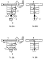
- a plurality of magnetoresistive elements 11, 12, 13 are stacked on a substrate, and recording conductors are arranged between the elements (FIGS. 3A and 3B).
- the magnetoresistive element as shown in FIG. 1B is used in FIGS. 3A and 3B.
- the elements 11, 12, 13 constitute a group of elements connected electrically in series.
- the group of elements is connected to a MOSFET, represented by a switching element 51.
- a rectifier element or the like e.g., a diode, a coulomb blockade element, or a tunnel diode may be used instead of the switching element.
- the nonlinear elements such as a switching element and a rectifier element, serve to electrically separate the adjacent groups of elements.
- sensitivity can be maintained, e.g., by dividing memory cells into blocks, each of which has a maximum of about 10,000 cells, and electrically separating one block from the other block.
- a magnetic field is applied to the element 11 basically through a word line 31 and a bit line 21.
- the bit line 21 and a word line 32 are used for the element 12, and the word line 32 and a bit line 22 are used for the element 13.
- a pair of recording conductors (the word line and the bit line) is arranged so as to sandwich each of the elements, and a synthetic magnetic field produced by a current flowing through the conductors is applied to the individual elements.
- the angle formed by the direction in which the word lines 31, 32 extend and the direction in which the bit lines 21, 22 extend is 90°, and the word lines and the bit lines are in the state of so-called "skew lines".
- the word lines 31, 32 are isolated electrically from each of the elements.
- the bit lines 21, 22 are connected electrically to each of the elements and also used as sense lines for reading information.
- the conductors including the word lines and the bit lines may be made of Cu, Al, or the like.
- the elements are connected in series, and the word lines and the bit lines are arranged alternately between the elements so that the word lines extend in a direction perpendicular to the direction of the bit lines.
- a magnetic field for recording information can be applied efficiently to each of the elements.
- the recording conductors are not limited to a single wire, and can be two or more parallel wires (FIG. 4).
- a memory shown in FIG. 4 includes word lines 31, 32 and bit lines 21, 22, each of which includes two wires.
- This embodiment is suitable for information recording at a high frequency (e.g., not less than 200 MHz) compared with the embodiment using the recording conductors of a single wire (FIGS. 3A and 3B).
- a high frequency e.g., not less than 200 MHz
- a constant potential e.g., a ground potential.
- Information may be written simultaneously into a plurality of elements.
- the elements 11, 13 are selected in writing information composed of a plurality of bits, recording errors caused by magnetic crosstalk or the like tend to be suppressed because no recording conductor is common to the elements 11, 13.
- a capacitor may be connected in parallel with the power supply and charged while a recording current is not generated. At the time of writing, a recording current may be supplied simultaneously from the power supply and the capacitor or the capacitor alone.
- the output change of the element 11 is ⁇ P 1
- the magnetic memory can have 7 memory values (FIG. 5).
- the magnetic memory can have 8 (2 3 ) memory values (FIG. 6).
- ⁇ R should be not less than a detectable minimum output value.
- the minimum ⁇ P (I ⁇ ⁇ R min ) is preferably not less than 50 mV to allow use of an inexpensive detecting element.
- the memory value obtained by N memory layers connected in series is 2 N - 1 at the maximum.
- the maximum output is not less than I ⁇ R min ⁇ 2 N - 1 , where I ⁇ R min is the minimum output change.
- the (M + 1)th smallest output change I ⁇ R M + 1 is not less than I ⁇ R M ⁇ 2, where I ⁇ R M is the Mth smallest output change (M is an integer of 1 to (N - 1)).
- the resistance change ⁇ R of each element is the product of the MR ratio and the element resistance R at a measuring bias or measuring current.
- the resistance change ⁇ R can be adjusted easily by controlling the element resistance R, e.g., the thickness of the tunnel insulating layer.
- a multivalued memory can be achieved not only by stacking magnetoresistive elements, but also by stacking a plurality of memory layers in a single element (FIG. 7).
- a tunnel layer 72, a free layer (memory layer) 73, and a bias tunnel layer 74 are added to the element in FIG. 1B, so that a single element can include two memory layers 3, 73.
- the tunnel layers 2, 72, the free layers 3, 73, and the bias tunnel layers 4, 74 are formed in the order mentioned on both sides of the pinned layer 1.
- a bit line 21 and a word line 31, which are in the state of skew lines, can be used for the application of a recording magnetic field to the memory layers 3, 73, and a switching element 51 can be used to select this memory.
- This magnetoresistive element may be stacked as shown in FIGS. 3A and 3B.
- the coercive force (magnetic switching field) of the memory layers can be varied to facilitate writing of information into the individual memory layers.
- the coercive force may be adjusted by controlling the material, the thickness, and the crystal structure of the memory layer, and further by forming the memory layer as a multilayer film.
- shape anisotropy may be imparted to the memory layer while taking into account the direction of the application of an external magnetic field.
- the thickness of a laminate 1-4, 72-74 is preferably not more than 500 nm so that a distance between the memory layer and each of the recording conductors is not excessively large.
- a circuit for detecting the output of a magnetic memory is connected to a comparative memory via a differential amplifier (FIG. 8).
- a difference in output between the magnetic memory and the comparative memory can be used to cancel the wiring resistance and the resistance of a reference element. This detecting circuit makes it easier to improve a S/N ratio.
- the same memory can be produced using rectifier elements 52, 53, 54, which are typified by a diode and a tunnel diode, instead of the switching element 51 (FIGS. 9A and 9B).
- the rectifier elements 52, 53, 54 are placed respectively between the recording conductors. Therefore, the resistance changes of magnetoresistive elements 11, 12, 13 can be read out individually.
- This memory uses word lines 31, 32 as well as bit lines 21, 22 (sense lines) for reading information. A resistance change between the word line 31 and the bit line 21 is read as a voltage/current change for the element 11, a resistance change between the bit line 21 and the word line 32 for the element 12, and a resistance change between the word line 32 and the bit line 22 for the element 13.
- This embodiment can improve a S/N ratio easily because the elements are separated electrically from one another.
- the element shown in FIG. 4 also may use a rectifier element 52 instead of the switching element 51 (FIG. 10).
- a magnetic memory of the present invention is not limited to the above configurations.
- further elements or memory layers may be stacked, and wiring may be changed appropriately.
- the magnetic memories may be arranged in matrix form with a predetermined number of memory columns and memory rows (FIG. 11).
- the magnetic memories 101, 102, ..., 201, 202, ..., 301, ..., 303, ... are located at the intersections of word lines 31, 131, 231, ... and bit lines 21, 121, 221, ....
- a recording current supplied to the recording conductors is controlled by switching elements 70, 170, 270, ..., 71, 171, 271, ... that are provided for each of the recording conductors. This control is performed by so-called coincident-current selection. For the example shown in FIG. 11, only the switching elements 70, 71 are in the on state to select the magnetic memory 101 located at the intersection of the word line 31 and the bit line 21, so that a recording magnetic field is applied to this memory.
- an inductive coupling current or capacitive coupling current may be generated between the recording conductors, resulting in magnetic crosstalk.
- bonding wires 81, 181, 281, ..., 91, 191, 291, ... are arranged between the recording conductors (FIG. 12).
- the bonding wires may be arranged between each of the recording conductors that lie in the thickness direction of the layers (FIG. 13).
- bonding wires 81, 82 are placed between magnetic memories 101, 201 , which are adjacent in the direction of bit lines 21, 22, so that the bonding wire 81 is arranged between word lines 31, 131 and the bonding wire 82 is arranged between word lines 32, 132.
- the bonding wires 81, 82 can suppress the occurrence of recording errors in a pair of adjacent magnetoresistive elements 11, 111 (12, 112; 13, 113).
- the bonding wires may be maintained at a predetermined constant potential, e.g., a ground potential.
- a switching magnetization curve of the free layer with uniaxial anisotropy may not be an ideal curve having fourth order symmetry (FIG. 14A), but can be an asteroid curve (FIG. 14B), which is obtained by enlarging the ideal curve in the direction of a hard axis of magnetization.
- This tendency becomes conspicuous in a memory layer whose anisotropy in the direction perpendicular to the film surface is not uniform, i.e., a memory layer including at least two magnetic films, such as a two-layer film including a soft magnetic film and a film with a high coercive force.
- the switching magnetization curve may have a multiaxially stable shape.
- a magnetization reversal region lies within one switching curve and out of the other switching curve (FIG. 17A).
- the application of a magnetic field indicated by a point A in FIG. 17A reverses only the magnetization of the memory layer having a switching curve a, while the application of a magnetic field indicated by a point B reverses only the magnetization of the memory layer having a switching curve b.
- the angle ⁇ between the easy axes can be expressed by an angle between the longitudinal directions of memory layers 3a, 3b (FIG. 17B). In this case, the angle ⁇ preferably ranges from 20° to 70°.
- the surface shape of the elements is illustrated as rectangular. However, the elements may have other surface shapes (FIGS. 19B to 19E).
- the angle between the easy axes preferably ranges from 20° to 90°.
- a memory device that includes magnetic memories in matrix form can suppress magnetic crosstalk by rotating the easy axes of magnetization of adjacent memory layers in different directions with respect to each other, i.e., by maintaining an angle between the easy axes preferably in the range of 20° to 90°, and more preferably in the range of 20° to 70° (FIG. 18).
- memory layers 201, 202, 203, ..., 211, 212, 213, ..., 221, 222, 223, ... are arranged so that the angle between the easy axes of magnetization of the memory layers that are adjacent in the in-plane direction of the layers ranges from 20° to 70°.
- the memory layers also may be arranged in such a manner that the easy axes of magnetization of the memory layers that are adjacent in the direction perpendicular to the plane of the layers (the thickness direction of the layers) are rotated with respect to each other (FIG. 16).
- a second memory layer plane 120 where memory layers are arranged in matrix form, is placed between a first memory layer plane 110 and a third memory layer plane 130.
- the second memory layer plane 120 has the easy axis of magnetization that differs from those of the adjacent memory layers located not only in the in-plane direction, but also in the direction perpendicular to that memory layer.
- the memory layer 222 and the adjacent memory layers (in both vertical and horizontal directions) 122, 221, 223, 322, 212, 232 are different from each other in direction of the easy axis of magnetization.
- the angle ⁇ between the easy axes is set to 90° in FIG. 16.
- the surface shape of the memory layer is illustrated as rectangular (FIG. 19A).
- the memory layer can have other surface shapes (FIGS. 19B to 19E).
- the square shape of a memory or the reliability of information storage can be improved by forming the memory layer in shapes such as a polygon with rounded corners (FIG. 19B), an ellipse (FIG. 19C), and a polygon having interior angles of more than 90° (FIGS. 19D, 19E).
- the switching element is turned off during magnetization reversal of the memory layer.
- the switching element is turned on when a sense current flows through the memory layer so as to read an output change in accordance with the magnetic state of the memory layer.
- a current flowing through the memory layer in its thickness direction can be used to determine the direction of rotation of the magnetization of the memory layer (FIG. 20A).
- a switching element 51 is turned on, then a current 63 flows through the element in the thickness direction of the layers, and a magnetic field 43 is produced and surrounds a memory layer (free layer) 3 in the in-plane direction, thereby reversing the magnetization of the memory layer 3.
- the magnetic field 43 contributes to smoother rotation of magnetization of the memory layer.
- Magnetic fields 41, 42 also may be produced by currents 61, 62 flowing through a bit line 21 and a word line 32 in the in-plane direction of the layers, respectively.
- the application of the current 62 through the word line 32 is started (ended) after the application of the current 63 through the switching element 51 is started (ended) (FIG. 20B).
- the magnetic field 43 produced by the current 63 induces rotation of the magnetization, and the magnetic field 42 produced by the current 62 directs the rotating magnetization to a predetermined direction.
- a current is separated from the bit line 21 (the sense line) and supplied to the switching element 51, so that the currents 61, 63 flow simultaneously.
- the magnetic fields 41, 43 are applied so as to cross over the magnetization direction 33 of the memory layer 3 (i.e., in the short side direction of the layer), making the magnetization direction 33 unstable (FIG. 20C).
- the fluctuation of magnetization that serves as a starting point for magnetization reversal occurs at both ends of the layer.
- the simultaneous application of the magnetic fields 41, 43 allows the fluctuation of magnetization to occur more easily at one end of the layer.
- the magnetization of the memory layer is rotated in a clockwise direction when viewed along the flow of the current 63, i.e., when viewed from the top of the element in FIG. 20A.
- the magnetization starts to rotate.
- the magnetic field 42 is applied in the opposite direction (antiparallel) to the original magnetization direction.
- the application of the magnetic fields 41, 42 is ended, so that the magnetization direction 33 is determined (FIG. 20C).
- the current 62 should flow through the word line 32 in the reverse direction.
- the currents 61, 63 should flow in the reverse direction.
- This element also can use the current 63 to read information from the memory layer 3.
- the writing/reading operation is the same either when a rectifier element 52 is used instead of the switching element 51 (FIGS. 21A, 21B) or when these elements are not used (FIG. 22A, 22B).
- FIGS. 21B and 22B show the reading operation with a sense current 64.
- a driving method of the present invention can be applied to both a conventional TMR element including a single memory layer and a magnetic memory including two or more memory layers that are stacked in the thickness direction of the layers.
- the memory layers have a higher density, and thus it may be difficult for a conventional driving method to smoothly reverse the magnetization of a certain memory layer. Therefore, the above driving method can provide a significant advantage.
- FIG. 23 shows an example of the basic circuit of the programmable or reconfigurable memory. Although this example employs the memory 100 shown in FIG. 7, available magnetic memories are not limited thereto.
- This circuit can be a nonvolatile programmable element by using a logic circuit as the load circuit, and can store, e.g., static images in a nonvolatile manner by using a display circuit as the load circuit.
- This circuit also can be used as a system LSI having these functions.
- Each of the FETs in FIG. 23 may be formed on a wafer.
- the magnetic memory is packaged in a magnetic shield. It is also preferable that a memory device (e.g., MRAM) and a system LSI are provided with a magnetic shield.
- the magnetic shield can suppress malfunction due to external magnetic noise.
- the magnetic shield may be made simply of a general magnetic material.
- An integrated memory was produced on a CMOS substrate with magnetic memories, each magnetic memory including a three-level magnetoresistive element as shown in FIG. 3.
- the integrated memory was sealed in a ceramic package, and the entire package was plated with a 100 ⁇ m thick NiFe film as a magnetic shield.
- the magnetic memories were arranged in matrix form as shown in FIG. 11, and comparative magnetic memories R1, R2, R3, ... were located for each memory column (FIG. 24).
- the comparative magnetic memories also included a three-level magnetoresistive element.
- the integrated memory included 256 ⁇ 256 magnetic memories (the total number of magnetoresistive elements was 256 ⁇ 256 ⁇ 3) and 256 comparative magnetic memories.
- a first magnetoresistive element of each of the magnetic memories was produced with the following layered structure:
- the figure in parentheses represents the thickness of each layer in nm, and the AlO thickness indicates the thickness of Al before oxidation (the thickness is expressed in the same manner in the following).
- AlO was a tunnel layer
- NiFe was a memory layer
- PtMn was an antiferromagnetic layer with which the magnetization of a pinned layer (CoFe/Ru/CoFe) was relatively hard to rotate.
- a second magnetoresistive element was produced in the same manner as the first element except that two layers of AlO(1.0) were replaced by AlO(1.06).
- a third magnetoresistive element was produced in the same manner as the first element except that two layers of AlO(1.0) were replaced by AlO(1.12).
- these elements were heat-treated in a magnetic field of 5 kOe at 280°C for 1 hour so as to impart unidirectional anisotropy to PtMn. Then, the surface shape of each layer in the individual elements was processed so that the long side direction was parallel to the direction of the unidirectional anisotropy. Specifically, the surface shape was 0.2 ⁇ m ⁇ 0.3 ⁇ m, and the long side direction of each layer was aligned in the horizontal direction of FIG. 3A.
- the outputs of the individual magnetoresistive elements other than wiring resistance and CMOS resistance were 40 mV for the first level, 80 mV for the second level, and 160 mV for the third level.
- a synthetic magnetic field produced by word lines and bit lines was used to record three bits for each magnetic memory including the three-level magnetoresistive element.
- the switching elements 70, 71 for the magnetic memory 101, into which information was to be written were addressed.
- the magnetizations of the elements 11, 12 were reversed simultaneously by allowing a current to flow through the word lines 31, 32 at the same time while applying a magnetic field to the elements in their short side direction.
- the simultaneous magnetization reversal of two or more elements was performed to reduce power consumption.
- the length of time that a current flows through the bit lines and the word lines (i.e., the pulse duration of a current) was 25 nsec (nanosecond) and controlled so that a current pulse from the word line arrived at the element 10 nsec after the arrival of a current pulse from the bit line.
- a sense current is split into the magnetic memory to be read and the comparative magnetic memory, and thus an additional switching element is necessary.
- separate circuits can be used for the magnetic memories and the comparative magnetic memories so as to reduce bias variations and lower the minimum value of a read voltage.
- a capacitor portion (not shown) may be located in parallel with each wiring and charged/discharged to lighten the load of power supply.
- a writing signal may differ from a reading signal with respect to a time base.
- a shift resistor or buffer memory can be used as a circuit that controls input/output signals.
- each magnetic memory including a magnetoresistive element having two memory layers 3, 73 as shown in FIG. 7.
- the integrated memory was provided with a magnetic shield similar to that of Example 1.
- the magnetoresistive element did not include the bias tunnel layers 4, 74.
- the magnetic memories were arranged in the same manner as Example 1 (FIG. 24).
- the total number of memories in this integrated memory was 256 ⁇ 256 ⁇ 2.
- an MRAM of 8 frames was produced.
- the magnetoresistive element had the following film configuration:
- AlO was a tunnel layer
- NiFe was a memory layer
- the multilayer film was heat-treated and then processed in view of unidirectional anisotropy, so that the long side direction of each layer was aligned in the horizontal direction of FIG. 7.
- a MR ratio was measured by applying a uniform magnetic field to the element with an external coil. The results showed that the coercive force of the two memory layers (NiFe) was about the same.
- the output changes of the individual memory layers caused by magnetization reversal other than wiring resistance and CMOS resistance were about 40 mV for the memory layer 73 on the lower electrode side and about 80 mV for the memory layer 3 on the upper electrode side.
- This multilayer film was formed so as to include NiFe(6) and NiFe(2) that differed in magnitude of shape anisotropy.
- a synthetic magnetic field produced by a word line and a bit line was used to write information individually into the memory layers 3, 73.
- Both magnetic switching curves of the memory layers have substantially the same shape as shown in FIG. 14A.
- a current-based magnetic switching curve is enlarged in the direction of the recording conductor that is located relatively close to the memory layers (FIG. 25). Therefore, the application of a synthetic current indicated by a point A reverses only the magnetization of the memory layer 3 having a magnetic switching curve p, while the application of a synthetic current indicated by a point B reverses only the magnetization of the memory layer 73 having a magnetic switching current q.
- This behavior can be used to write information into any memory layer selected from a plurality of memory layers in a single magnetoresistive element.
- the writing and reading operations can be performed in the same manner as Example 1.
- This MRAM allows information to be read simultaneously from one element for each of the 8 basic frames, so that memories with a total of 2 ⁇ 8 bits can be read at the same time.
- An integrated memory was produced on a glass substrate with magnetic memories, each magnetic memory including a three-level magnetoresistive element as shown in FIG. 9.
- the integrated memory was provided with a magnetic shield similar to that of Example 1.
- the magnetic memories were arranged as shown in FIG. 24.
- the integrated memory included 256 ⁇ 256 magnetic memories (the total number of magnetoresistive elements was 256 ⁇ 256 ⁇ 3). By using this group of magnetic memories as a frame, an MRAM of 8 frames was produced.
- first, second, and third magnetoresistive elements had the following film configuration:
- AlO was a tunnel layer
- Fe was a memory layer
- AlO in contact with Ta was a bias tunnel layer.
- the multilayer film was heat-treated and then processed in view of unidirectional anisotropy, so that the long side direction of each layer was aligned in the horizontal direction of FIG. 9A.
- Diodes having a p-i-n structure in the forward direction were formed between each of the magnetoresistive elements as the rectifier elements 52, 53, 54.
- the layers in the pin structure were deposited by CVD.
- the i layer was formed of SiH 4 and H 2 .
- "0.5%" is a percentage relative to H 2 .
- a Ti buffer layer was formed between the diode and the magnetoresistive element or the wiring.
- the outputs of the individual magnetoresistive elements other than wiring resistance and diode resistance were 120 mV
- the reading operation will be described with reference to FIGS. 9 and 24.
- the magnetic memory 101 from which information was to be read, and the comparative magnetic memory R1 were addressed.
- the word lines 31, 32 were maintained at a ground potential, so that a sense current flowing between the bit line 22 and the word line 32 was the same in magnitude as a sense current flowing between the bit line 21 and the word line 31.
- a memory value of the element 11 was determined first, followed by a memory value of the element 12. In this manner, the memory values of two magnetoresistive elements 11, 12 of a single magnetic memory 101 were read.
- An integrated memory was produced on a glass substrate with magnetic memories, each magnetic memory including a magnetoresistive element having two memory layers as shown in FIG. 10.
- the integrated memory was provided with a magnetic shield similar to that of Example 1.
- the magnetic memories were arranged as shown in FIG. 24.
- the integrated memory included 256 ⁇ 256 magnetic memories (the total number of memory layers was 256 ⁇ 256 ⁇ 2). By using this group of magnetic memories as a frame, an MRAM of 8 frames was produced.
- the magnetoresistive element had the following film configuration:
- AlO was a tunnel layer
- Fe was a memory layer
- AlO in contact with Ta was a bias tunnel layer.
- the multilayer film was heat-treated and then processed in view of unidirectional anisotropy, so that the long side direction of each layer was aligned in the horizontal direction of FIG. 10.
- a MR ratio was measured by applying a uniform magnetic field to the element with an external coil. The results showed that the coercive force of the two memory layers (Fe) was about the same.
- the output changes of the individual memory layers caused by magnetization reversal other than wiring resistance and diode resistance were about 40 mV for the memory layer 73 on the lower electrode side and about 80 mV for the memory layer 3 on the upper electrode side. The output changes were determined in the same manner as Example 2.
- Example 2 information was written individually into the memory layers of a single element, and the information was read from the memory layers by allowing a sense current to flow from the bit line 21, which also was used as the sense line, to the word line 31.
- An integrated memory was produced on a CMOS substrate with magnetic memories, each magnetic memory including a multilevel magnetoresistive element as shown in FIG. 3. This example used a two-level magnetoresistive element.
- the integrated memory was provided with a magnetic shield similar to that of Example 1.
- the magnetic memories were arranged as shown in FIG. 24.
- the integrated memory included 256 ⁇ 256 magnetic memories (the total number of magnetoresistive elements was 256 ⁇ 256 ⁇ 2).
- a first magnetoresistive element of each of the magnetic memories was produced with the following layered structure:
- AlO was a tunnel layer
- CoFe(0.5)/NiFe(2)/CoFe(0.5) was a memory layer.
- the first element was heat-treated under the same conditions as those in Example 1 so as to impart unidirectional anisotropy to PtMn. Then, the surface shape of each layer was processed to 0.2 ⁇ m ⁇ 0.3 ⁇ m so that the long side direction was parallel to the direction of the unidirectional anisotropy (i.e., the long side direction of each layer was aligned in the horizontal direction of FIG. 3).
- unidirectional anisotropy was imparted perpendicular to the longitudinal direction of PtMn by depositing IrMn in a magnetic field. Then, the surface shape of each layer was processed to 0.2 ⁇ m ⁇ 0.3 ⁇ m so that the long side direction was parallel to the direction of the unidirectional anisotropy (i.e., the short side direction of each layer was aligned in the horizontal direction of FIG. 3).
- the integrated memory thus produced was referred to as "memory A".
- a first element was produced in the same manner as described above, and a second element was produced in the same manner as the first element except that AlO(1) was replaced by AlO(1.06).
- the integrated memory thus produced was referred to as "memory B".
- the direction of unidirectional anisotropy and the long side direction of each layer in the first element matched with those in the second element (i.e., the long side directions of the first and second elements were aligned in the horizontal direction of FIG. 3).
- the outputs of the individual magnetoresistive elements other than wiring resistance and CMOS resistance were 60 mV for the first level and 120 mV for the second level.
- magnetization reversal was repeated in such a manner that a magnetic field produced by a bit line 21 was applied to the first element in the short side direction of each layer, and a magnetic field produced by a word line 31 was applied further to the first element. Then, the probability of recording errors in the second element was measured. The results showed that 10 -8 /cycle for the memory A and 10 -6 /cycle for the memory B. Here, the recording errors included errors during reading.
- the memories I to III used a multilayer film as a memory layer.
- NiFe(2)/Ru(0.9)/NiFe(4) was a memory layer.
- NiFe(2)/Ru(0.9)/NiFe(4)/Ru(0.9)/NiFe(4) was a memory layer.
- NiFe(1)/CoFe(1) was a memory layer.
- the memory IV included NiFe(2) as a memory layer.
- the first element of each of the memories was heat-treated in a magnetic field of 5 kOe at 280°C for 1 hour so as to impart unidirectional anisotropy to PtMn. Then, the shape of the element for each layer was processed to 0.2 ⁇ m ⁇ 0.3 ⁇ m so that the long side direction was parallel to the direction of the unidirectional anisotropy (i.e., the long side direction of each layer was aligned in the horizontal direction of FIG. 3A).
- unidirectional anisotropy was imparted perpendicular to the longitudinal direction of PtMn by depositing IrMn in a magnetic field. Then, the shape of the element for each layer was processed to 0.2 ⁇ m ⁇ 0.3 ⁇ m so that the long side direction was parallel to the direction of the unidirectional anisotropy (i.e., the short side direction of each layer was aligned in the horizontal direction of FIG. 3A).
- the outputs of the individual elements other than wiring resistance and CMOS resistance were 60 mV for the first level and 120 mV for the second level.
- the switching magnetization curve of the memory layer deviates from a simple curve having fourth order symmetry. This may lead to a reduction in recording errors.
- An MRAM was produced on a CMOS substrate with magnetoresistive elements arranged in matrix form, each magnetoresistive element having a configuration as shown in FIG. 27. This MRAM was used to study recording methods.
- the magnetoresistive element had the following configuration:
- AlO(1.3) was a bias tunnel layer 4
- Fe(2) was a memory layer 3
- AlO(1.0) was a tunnel layer 2
- CoFe(3)/Ru(0.9)/CoFe(3) was a pinned layer 1.
- PtMn(20) was an antiferromagnetic layer (not shown).
- the multilayer film was heat-treated in a magnetic field of 5 kOe at 280°C for 1 hour so as to impart unidirectional anisotropy to PtMn. Then, the shape of the element for each layer was processed to 0.1 ⁇ m ⁇ 0.15 ⁇ m so that the long side direction was parallel to the direction of the unidirectional anisotropy (i.e., the long side direction of each layer was aligned in the horizontal direction of FIG. 27).
- the currents 61a, 61b flowed through the bit line 21 in opposite directions so that the direction of a magnetic field produced by the current before splitting was opposite to the direction of a magnetic field produced by the current after splitting, recording errors were not reduced.
- the current flowing through the bit line before splitting is relatively large compared with the current after splitting. Therefore, the magnetic field produced by the current before splitting may prevent the current that perpendicularly flows through the memory layer from assisting the magnetization reversal.
Landscapes
- Engineering & Computer Science (AREA)
- Computer Hardware Design (AREA)
- Chemical & Material Sciences (AREA)
- Nanotechnology (AREA)
- Physics & Mathematics (AREA)
- Mathematical Physics (AREA)
- Theoretical Computer Science (AREA)
- Crystallography & Structural Chemistry (AREA)
- Hall/Mr Elements (AREA)
- Mram Or Spin Memory Techniques (AREA)
- Thin Magnetic Films (AREA)
- Semiconductor Memories (AREA)
Applications Claiming Priority (3)
| Application Number | Priority Date | Filing Date | Title |
|---|---|---|---|
| JP2001184480 | 2001-06-19 | ||
| JP2001184480 | 2001-06-19 | ||
| PCT/JP2002/006093 WO2002103798A1 (fr) | 2001-06-19 | 2002-06-19 | Memoire magnetique et procede de commande associe, ainsi qu'appareil de memoire magnetique comprenant celle-ci |
Publications (2)
| Publication Number | Publication Date |
|---|---|
| EP1398835A1 true EP1398835A1 (fr) | 2004-03-17 |
| EP1398835A4 EP1398835A4 (fr) | 2006-03-29 |
Family
ID=19024233
Family Applications (1)
| Application Number | Title | Priority Date | Filing Date |
|---|---|---|---|
| EP02736165A Withdrawn EP1398835A4 (fr) | 2001-06-19 | 2002-06-19 | Memoire magnetique et procede de commande associe, ainsi qu'appareil de memoire magnetique comprenant celle-ci |
Country Status (4)
| Country | Link |
|---|---|
| US (1) | US6950333B2 (fr) |
| EP (1) | EP1398835A4 (fr) |
| CN (1) | CN1270323C (fr) |
| WO (1) | WO2002103798A1 (fr) |
Cited By (7)
| Publication number | Priority date | Publication date | Assignee | Title |
|---|---|---|---|---|
| EP1403875A3 (fr) * | 2002-09-30 | 2004-12-01 | Kabushiki Kaisha Toshiba | Elément magnétorésistif et mémoire magnétique rendant possible une haute densité de cellules |
| EP1653516A2 (fr) | 2004-10-28 | 2006-05-03 | Samsung Electronics Co., Ltd. | Mémoire vive magnétorésistante |
| EP1653475A1 (fr) * | 2004-10-27 | 2006-05-03 | Samsung Electronics Co., Ltd. | Dispositif de mémoire magnétique à accès aléatoire multi-bits et son procédé d'écriture |
| WO2007015030A1 (fr) * | 2005-08-03 | 2007-02-08 | Stmicroelectronics Sa | Resistance variable |
| DE102005040557A1 (de) * | 2005-08-26 | 2007-03-01 | Infineon Technologies Ag | Integrierte Speicherschaltung mit einem resistiven Speicherelement sowie ein Verfahren zur Herstellung einer solchen Speicherschaltung |
| US7336528B2 (en) | 2004-10-27 | 2008-02-26 | Samsung Electronics Co., Ltd. | Advanced multi-bit magnetic random access memory device |
| EP1993098A1 (fr) * | 2007-05-08 | 2008-11-19 | Honeywell International Inc. | Cellule MRAM avec éléments de stockage multiples |
Families Citing this family (17)
| Publication number | Priority date | Publication date | Assignee | Title |
|---|---|---|---|---|
| JP3906212B2 (ja) * | 2003-03-11 | 2007-04-18 | 株式会社東芝 | 磁気ランダムアクセスメモリ |
| KR100612854B1 (ko) * | 2004-07-31 | 2006-08-21 | 삼성전자주식회사 | 스핀차지를 이용한 자성막 구조체와 그 제조 방법과 그를구비하는 반도체 장치 및 이 장치의 동작방법 |
| US7916520B2 (en) * | 2004-08-25 | 2011-03-29 | Nec Corporation | Memory cell and magnetic random access memory |
| US7813164B2 (en) * | 2004-08-26 | 2010-10-12 | Nec Corporation | Magneto resistance element and magnetic random access memory |
| US7272028B2 (en) * | 2005-05-27 | 2007-09-18 | Infineon Technologies Ag | MRAM cell with split conductive lines |
| JP2006332527A (ja) * | 2005-05-30 | 2006-12-07 | Renesas Technology Corp | 磁気記憶素子 |
| US7345855B2 (en) * | 2005-09-07 | 2008-03-18 | International Business Machines Corporation | Tunnel barriers based on rare earth element oxides |
| US8719610B2 (en) | 2008-09-23 | 2014-05-06 | Qualcomm Incorporated | Low power electronic system architecture using non-volatile magnetic memory |
| US7940551B2 (en) | 2008-09-29 | 2011-05-10 | Seagate Technology, Llc | STRAM with electronically reflective insulative spacer |
| US7826256B2 (en) * | 2008-09-29 | 2010-11-02 | Seagate Technology Llc | STRAM with compensation element |
| US8411494B2 (en) | 2009-07-21 | 2013-04-02 | Alexander Mikhailovich Shukh | Three-dimensional magnetic random access memory with high speed writing |
| US8331141B2 (en) | 2009-08-05 | 2012-12-11 | Alexander Mikhailovich Shukh | Multibit cell of magnetic random access memory with perpendicular magnetization |
| WO2011087038A1 (fr) | 2010-01-13 | 2011-07-21 | 株式会社日立製作所 | Mémoire magnétique, procédé pour produire une mémoire magnétique et procédé de commande de mémoire magnétique |
| US8988934B2 (en) | 2010-07-27 | 2015-03-24 | Alexander Mikhailovich Shukh | Multibit cell of magnetic random access memory with perpendicular magnetization |
| US9070456B2 (en) | 2011-04-07 | 2015-06-30 | Tom A. Agan | High density magnetic random access memory |
| US8976577B2 (en) | 2011-04-07 | 2015-03-10 | Tom A. Agan | High density magnetic random access memory |
| JP2021044444A (ja) * | 2019-09-12 | 2021-03-18 | キオクシア株式会社 | 磁気記憶装置 |
Citations (2)
| Publication number | Priority date | Publication date | Assignee | Title |
|---|---|---|---|---|
| US5982660A (en) * | 1998-08-27 | 1999-11-09 | Hewlett-Packard Company | Magnetic memory cell with off-axis reference layer orientation for improved response |
| JP2001084756A (ja) * | 1999-09-17 | 2001-03-30 | Sony Corp | 磁化駆動方法、磁気機能素子および磁気装置 |
Family Cites Families (11)
| Publication number | Priority date | Publication date | Assignee | Title |
|---|---|---|---|---|
| JP3282943B2 (ja) * | 1995-04-28 | 2002-05-20 | 松下電器産業株式会社 | メモリー素子 |
| DE19744095A1 (de) * | 1997-10-06 | 1999-04-15 | Siemens Ag | Speicherzellenanordnung |
| US5930164A (en) | 1998-02-26 | 1999-07-27 | Motorola, Inc. | Magnetic memory unit having four states and operating method thereof |
| JPH11354728A (ja) * | 1998-06-09 | 1999-12-24 | Canon Inc | 磁性薄膜メモリおよびその記録再生駆動方法 |
| JP2001015611A (ja) | 1999-07-01 | 2001-01-19 | Mitsubishi Electric Corp | 半導体装置の製造方法 |
| US6169689B1 (en) * | 1999-12-08 | 2001-01-02 | Motorola, Inc. | MTJ stacked cell memory sensing method and apparatus |
| TW495745B (en) | 2000-03-09 | 2002-07-21 | Koninkl Philips Electronics Nv | Magnetic field element having a biasing magnetic layer structure |
| JP2001338487A (ja) * | 2000-03-24 | 2001-12-07 | Sharp Corp | 磁気メモリ、磁気メモリの製造方法 |
| JP4050446B2 (ja) * | 2000-06-30 | 2008-02-20 | 株式会社東芝 | 固体磁気メモリ |
| US6587370B2 (en) * | 2000-11-01 | 2003-07-01 | Canon Kabushiki Kaisha | Magnetic memory and information recording and reproducing method therefor |
| JP2002246567A (ja) * | 2001-02-14 | 2002-08-30 | Toshiba Corp | 磁気ランダムアクセスメモリ |
-
2002
- 2002-06-19 EP EP02736165A patent/EP1398835A4/fr not_active Withdrawn
- 2002-06-19 WO PCT/JP2002/006093 patent/WO2002103798A1/fr not_active Application Discontinuation
- 2002-06-19 CN CNB028121341A patent/CN1270323C/zh not_active Expired - Fee Related
-
2003
- 2003-10-24 US US10/695,731 patent/US6950333B2/en not_active Expired - Lifetime
Patent Citations (2)
| Publication number | Priority date | Publication date | Assignee | Title |
|---|---|---|---|---|
| US5982660A (en) * | 1998-08-27 | 1999-11-09 | Hewlett-Packard Company | Magnetic memory cell with off-axis reference layer orientation for improved response |
| JP2001084756A (ja) * | 1999-09-17 | 2001-03-30 | Sony Corp | 磁化駆動方法、磁気機能素子および磁気装置 |
Non-Patent Citations (2)
| Title |
|---|
| PATENT ABSTRACTS OF JAPAN vol. 2000, no. 20, 10 July 2001 (2001-07-10) -& JP 2001 084756 A (SONY CORP), 30 March 2001 (2001-03-30) & US 6 483 741 B1 (IWASAKI YOH ET AL) 19 November 2002 (2002-11-19) * |
| See also references of WO02103798A1 * |
Cited By (14)
| Publication number | Priority date | Publication date | Assignee | Title |
|---|---|---|---|---|
| US7470963B2 (en) | 2002-09-30 | 2008-12-30 | Kabushiki Kaisha Toshiba | Magnetoresistive element and magnetic memory |
| US6949779B2 (en) | 2002-09-30 | 2005-09-27 | Kabushiki Kaisha Toshiba | Magnetoresistive element and magnetic memory |
| EP1403875A3 (fr) * | 2002-09-30 | 2004-12-01 | Kabushiki Kaisha Toshiba | Elément magnétorésistif et mémoire magnétique rendant possible une haute densité de cellules |
| EP1653475A1 (fr) * | 2004-10-27 | 2006-05-03 | Samsung Electronics Co., Ltd. | Dispositif de mémoire magnétique à accès aléatoire multi-bits et son procédé d'écriture |
| US7336528B2 (en) | 2004-10-27 | 2008-02-26 | Samsung Electronics Co., Ltd. | Advanced multi-bit magnetic random access memory device |
| US7567453B2 (en) | 2004-10-27 | 2009-07-28 | Samsung Electronics Co., Ltd. | Advanced multi-bit magnetic random access memory device |
| EP1653516A2 (fr) | 2004-10-28 | 2006-05-03 | Samsung Electronics Co., Ltd. | Mémoire vive magnétorésistante |
| EP1653516A3 (fr) * | 2004-10-28 | 2007-10-10 | Samsung Electronics Co., Ltd. | Mémoire vive magnétorésistante |
| US7463509B2 (en) | 2004-10-28 | 2008-12-09 | Samsung Electronics Co., Ltd. | Magneto-resistive RAM having multi-bit cell array structure |
| WO2007015030A1 (fr) * | 2005-08-03 | 2007-02-08 | Stmicroelectronics Sa | Resistance variable |
| FR2889623A1 (fr) * | 2005-08-03 | 2007-02-09 | St Microelectronics Sa | Resistance variable |
| DE102005040557A1 (de) * | 2005-08-26 | 2007-03-01 | Infineon Technologies Ag | Integrierte Speicherschaltung mit einem resistiven Speicherelement sowie ein Verfahren zur Herstellung einer solchen Speicherschaltung |
| US7539047B2 (en) | 2007-05-08 | 2009-05-26 | Honeywell International, Inc. | MRAM cell with multiple storage elements |
| EP1993098A1 (fr) * | 2007-05-08 | 2008-11-19 | Honeywell International Inc. | Cellule MRAM avec éléments de stockage multiples |
Also Published As
| Publication number | Publication date |
|---|---|
| WO2002103798A1 (fr) | 2002-12-27 |
| US6950333B2 (en) | 2005-09-27 |
| US20040085807A1 (en) | 2004-05-06 |
| EP1398835A4 (fr) | 2006-03-29 |
| CN1270323C (zh) | 2006-08-16 |
| CN1529910A (zh) | 2004-09-15 |
Similar Documents
| Publication | Publication Date | Title |
|---|---|---|
| US6950333B2 (en) | Magnetic memory and method for driving the same, and magnetic memory device using the same | |
| US6914807B2 (en) | Magnetic logic element and magnetic logic element array | |
| CN100407470C (zh) | 磁开关元件和磁存储器 | |
| JP4371781B2 (ja) | 磁気セル及び磁気メモリ | |
| JP3824600B2 (ja) | 磁気抵抗効果素子および磁気メモリ | |
| US8331141B2 (en) | Multibit cell of magnetic random access memory with perpendicular magnetization | |
| JP3863484B2 (ja) | 磁気抵抗効果素子および磁気メモリ | |
| US7973349B2 (en) | Magnetic device having multilayered free ferromagnetic layer | |
| US6839273B2 (en) | Magnetic switching device and magnetic memory using the same | |
| US7714399B2 (en) | Magnetic memory element and magnetic memory apparatus | |
| US7042762B2 (en) | Magnetic element and magnetic element array | |
| JP3699954B2 (ja) | 磁気メモリ | |
| JP6972542B2 (ja) | スピン流磁化反転素子、磁気抵抗効果素子および磁気メモリ | |
| JP2009094104A (ja) | 磁気抵抗素子 | |
| JP2003209226A (ja) | 磁気メモリ | |
| KR20080029852A (ko) | 자기저항 효과 소자 및 자기저항 랜덤 액세스 메모리 | |
| JP2002204010A (ja) | 磁気抵抗素子 | |
| KR20040029257A (ko) | 자기저항 소자 및 자기 메모리 장치 | |
| JP6411186B2 (ja) | 磁気抵抗素子および磁気メモリ | |
| JP2003298023A (ja) | 磁気メモリ及び磁気メモリ装置 | |
| JP3527230B2 (ja) | 磁気メモリの駆動方法 | |
| US20050122828A1 (en) | Magnetic switching device and memory using the same | |
| JP2002299574A (ja) | 磁気記憶素子、磁気記憶装置および携帯端末装置 | |
| JP4329505B2 (ja) | 磁気メモリを用いた磁気メモリ装置 | |
| JP2002299725A (ja) | 磁気抵抗デバイス |
Legal Events
| Date | Code | Title | Description |
|---|---|---|---|
| PUAI | Public reference made under article 153(3) epc to a published international application that has entered the european phase |
Free format text: ORIGINAL CODE: 0009012 |
|
| 17P | Request for examination filed |
Effective date: 20031016 |
|
| AK | Designated contracting states |
Kind code of ref document: A1 Designated state(s): AT BE CH CY DE DK ES FI FR GB GR IE IT LI LU MC NL PT SE TR |
|
| AX | Request for extension of the european patent |
Extension state: AL LT LV MK RO SI |
|
| RIN1 | Information on inventor provided before grant (corrected) |
Inventor name: KAWASHIMA, YOSHIO Inventor name: SUGITA, YASUNARI Inventor name: SATOMI, MITSUO Inventor name: ODAGAWA, AKIHIRO Inventor name: MATSUKAWA, NOZOMU Inventor name: HIRAMOTO, MASAYOSHI |
|
| RIN1 | Information on inventor provided before grant (corrected) |
Inventor name: KAWASHIMA, YOSHIO Inventor name: SUGITA, YASUNARI Inventor name: SATOMI, MITSUO Inventor name: ODAGAWA, AKIHIRO Inventor name: MATSUKAWA, NOZOMU Inventor name: HIRAMOTO, MASAYOSHI |
|
| A4 | Supplementary search report drawn up and despatched |
Effective date: 20060210 |
|
| RIC1 | Information provided on ipc code assigned before grant |
Ipc: G11C 11/16 20060101ALI20060206BHEP Ipc: G11C 11/15 20060101ALI20060206BHEP Ipc: H01L 27/105 20060101AFI20030107BHEP |
|
| GRAP | Despatch of communication of intention to grant a patent |
Free format text: ORIGINAL CODE: EPIDOSNIGR1 |
|
| STAA | Information on the status of an ep patent application or granted ep patent |
Free format text: STATUS: THE APPLICATION IS DEEMED TO BE WITHDRAWN |
|
| 18D | Application deemed to be withdrawn |
Effective date: 20070914 |