EP1361604A1 - Einrichtung und verfahren zur behandlung - Google Patents
Einrichtung und verfahren zur behandlung Download PDFInfo
- Publication number
- EP1361604A1 EP1361604A1 EP02716335A EP02716335A EP1361604A1 EP 1361604 A1 EP1361604 A1 EP 1361604A1 EP 02716335 A EP02716335 A EP 02716335A EP 02716335 A EP02716335 A EP 02716335A EP 1361604 A1 EP1361604 A1 EP 1361604A1
- Authority
- EP
- European Patent Office
- Prior art keywords
- gas
- holes
- supplied
- diffusion
- grooves
- Prior art date
- Legal status (The legal status is an assumption and is not a legal conclusion. Google has not performed a legal analysis and makes no representation as to the accuracy of the status listed.)
- Granted
Links
Images


Classifications
-
- H—ELECTRICITY
- H01—ELECTRIC ELEMENTS
- H01L—SEMICONDUCTOR DEVICES NOT COVERED BY CLASS H10
- H01L21/00—Processes or apparatus adapted for the manufacture or treatment of semiconductor or solid state devices or of parts thereof
- H01L21/02—Manufacture or treatment of semiconductor devices or of parts thereof
- H01L21/04—Manufacture or treatment of semiconductor devices or of parts thereof the devices having at least one potential-jump barrier or surface barrier, e.g. PN junction, depletion layer or carrier concentration layer
- H01L21/18—Manufacture or treatment of semiconductor devices or of parts thereof the devices having at least one potential-jump barrier or surface barrier, e.g. PN junction, depletion layer or carrier concentration layer the devices having semiconductor bodies comprising elements of Group IV of the Periodic System or AIIIBV compounds with or without impurities, e.g. doping materials
- H01L21/30—Treatment of semiconductor bodies using processes or apparatus not provided for in groups H01L21/20 - H01L21/26
- H01L21/31—Treatment of semiconductor bodies using processes or apparatus not provided for in groups H01L21/20 - H01L21/26 to form insulating layers thereon, e.g. for masking or by using photolithographic techniques; After treatment of these layers; Selection of materials for these layers
-
- C—CHEMISTRY; METALLURGY
- C23—COATING METALLIC MATERIAL; COATING MATERIAL WITH METALLIC MATERIAL; CHEMICAL SURFACE TREATMENT; DIFFUSION TREATMENT OF METALLIC MATERIAL; COATING BY VACUUM EVAPORATION, BY SPUTTERING, BY ION IMPLANTATION OR BY CHEMICAL VAPOUR DEPOSITION, IN GENERAL; INHIBITING CORROSION OF METALLIC MATERIAL OR INCRUSTATION IN GENERAL
- C23C—COATING METALLIC MATERIAL; COATING MATERIAL WITH METALLIC MATERIAL; SURFACE TREATMENT OF METALLIC MATERIAL BY DIFFUSION INTO THE SURFACE, BY CHEMICAL CONVERSION OR SUBSTITUTION; COATING BY VACUUM EVAPORATION, BY SPUTTERING, BY ION IMPLANTATION OR BY CHEMICAL VAPOUR DEPOSITION, IN GENERAL
- C23C16/00—Chemical coating by decomposition of gaseous compounds, without leaving reaction products of surface material in the coating, i.e. chemical vapour deposition [CVD] processes
- C23C16/44—Chemical coating by decomposition of gaseous compounds, without leaving reaction products of surface material in the coating, i.e. chemical vapour deposition [CVD] processes characterised by the method of coating
- C23C16/455—Chemical coating by decomposition of gaseous compounds, without leaving reaction products of surface material in the coating, i.e. chemical vapour deposition [CVD] processes characterised by the method of coating characterised by the method used for introducing gases into reaction chamber or for modifying gas flows in reaction chamber
- C23C16/45563—Gas nozzles
- C23C16/45565—Shower nozzles
-
- C—CHEMISTRY; METALLURGY
- C23—COATING METALLIC MATERIAL; COATING MATERIAL WITH METALLIC MATERIAL; CHEMICAL SURFACE TREATMENT; DIFFUSION TREATMENT OF METALLIC MATERIAL; COATING BY VACUUM EVAPORATION, BY SPUTTERING, BY ION IMPLANTATION OR BY CHEMICAL VAPOUR DEPOSITION, IN GENERAL; INHIBITING CORROSION OF METALLIC MATERIAL OR INCRUSTATION IN GENERAL
- C23C—COATING METALLIC MATERIAL; COATING MATERIAL WITH METALLIC MATERIAL; SURFACE TREATMENT OF METALLIC MATERIAL BY DIFFUSION INTO THE SURFACE, BY CHEMICAL CONVERSION OR SUBSTITUTION; COATING BY VACUUM EVAPORATION, BY SPUTTERING, BY ION IMPLANTATION OR BY CHEMICAL VAPOUR DEPOSITION, IN GENERAL
- C23C16/00—Chemical coating by decomposition of gaseous compounds, without leaving reaction products of surface material in the coating, i.e. chemical vapour deposition [CVD] processes
- C23C16/44—Chemical coating by decomposition of gaseous compounds, without leaving reaction products of surface material in the coating, i.e. chemical vapour deposition [CVD] processes characterised by the method of coating
- C23C16/455—Chemical coating by decomposition of gaseous compounds, without leaving reaction products of surface material in the coating, i.e. chemical vapour deposition [CVD] processes characterised by the method of coating characterised by the method used for introducing gases into reaction chamber or for modifying gas flows in reaction chamber
-
- H—ELECTRICITY
- H01—ELECTRIC ELEMENTS
- H01J—ELECTRIC DISCHARGE TUBES OR DISCHARGE LAMPS
- H01J37/00—Discharge tubes with provision for introducing objects or material to be exposed to the discharge, e.g. for the purpose of examination or processing thereof
- H01J37/32—Gas-filled discharge tubes
- H01J37/32431—Constructional details of the reactor
- H01J37/3244—Gas supply means
Definitions
- the present invention relates to a plasma process system and a plasma process method which perform processes, such as film deposition and etching, using a plasma.
- a plasma process system which processes the surface of a substrate, such as a semiconductor wafer, using a plasma is used in a fabrication process for a liquid crystal display or the like.
- plasma process systems there are, for example, a plasma etching system which performs etching on a substrate and a plasma CVD system which performs chemical vapor deposition (Chemical Vapor Deposition: CVD).
- CVD chemical Vapor Deposition
- a parallel plate plasma process system is widely used because it has an excellent process uniformity and its system structure is relatively simple.
- a parallel plate plasma process system has two parallel plate electrodes faces each other vertically in parallel to each other.
- a substrate is mounted on a lower electrode of the two electrodes.
- the upper electrode has an electrode plate facing the lower electrode and having multiple gas holes, and has a so-called shower head structure.
- the upper electrode is connected to a supply source for a process gas so that at the time of processing, the process gas is supplied between two electrodes through the gas holes in the electrode plate.
- the process gas supplied between the electrodes is turned into a plasma by the application of high-frequency power to the electrodes, and the surface of the substrate is processed by the plasma.
- the upper electrode of the shower head structure has a hollow diffusion portion inside.
- the diffusion portion is provided in such a way as to cover one side of the electrode plate and the process gas is diffused into multiple gas holes by the diffusion portion.
- it is important to lead the gas to the gas holes by controlling the diffusion of the process gas at the diffusion portion.
- a structure which separates the diffusion portion 21 into a plurality of areas and supplies the process gas to the individual areas has been developed. According to this structure, it is possible to control the amount of the process gas to be ejected from the gas holes that communicate with the individual areas by adjusting the amount of the process gas to be supplied to the individual areas. Accordingly, a process with high uniformity can be performed on the substrate surface.
- a process system (1) according to the first aspect of the invention comprises:
- the first diffusion portion may be comprised of a disk-like member (21, 40, 41) having a plurality of grooves (30, 50, 53) formed in one side thereof and communicating with one another and through holes (31a, 52, 54) formed in the plurality of grooves (30, 50, 53) and led to the other side.
- At least one of the grooves (30, 53) may be provided at positions to which the gas is supplied, and, for example, the gas supplied to the at least one groove (30, 53) may be dispersed to the other grooves (30a, 54) and flow out to the other side through the through holes (31a, 54) respectively provided in the other grooves (30, 53).
- the second diffusion portion may be comprised of a disk-like member (21, 41) having a groove (32, 57) formed in one side thereof and placed over the supply plate (19) to form a hollow portion between itself and the one side and through holes (31a, 54) formed in the groove (32, 57) and led to the other side, and, for example, the gas from the first diffusion portion may be supplied to the hollow portion via the through holes (31a, 54).
- the disk-like member (21, 41) constituting the second diffusion portion may be made of, for example, a same member as the disk-like member (21, 41) constituting the first diffusion portion, and, for example, the groove (32, 57) constituting the second diffusion portion and the grooves (30) constituting the first diffusion portion may be formed in opposite sides of the member.
- the process system (1) according to the first aspect may further comprise a partition member (56) which is provided in the groove (57) constituting the second diffusion portion and separate the hollow portion into a plurality of areas, and, for example, the first diffusion portion may supply the gas, dispersed, to the plurality of areas.
- a partition member (56) which is provided in the groove (57) constituting the second diffusion portion and separate the hollow portion into a plurality of areas, and, for example, the first diffusion portion may supply the gas, dispersed, to the plurality of areas.
- the first diffusion portion may be comprised of a cylindrical member (20) having a plurality of linear holes (71, 72) communicating with one another, formed by boring and sealing end portions of bored portions, for example, at least one of the holes (71, 72) may be supplied with the gas and the gas supplied to the at least one hole (71, 72) may be dispersed to the other holes (71, 72).
- the cylindrical member (20) may have connection holes (73b, 74b) provided in such a way as to be led to the other holes (71, 72) from its one side, and the gas supplied to the other holes (71, 72) may be supplied to, for example, the second diffusion portion from the connection holes (73b, 74b).
- a process method uses a process system (1) comprising a chamber (2) and a supply plate (19) which has a plurality of gas holes (22) and supplies a process gas into the chamber (2) through the gas holes (22), and comprises:
- Fig. 1 shows a cross-sectional view of a plasma process system 1 according to the first embodiment of the invention.
- the plasma process system 1 has an approximately cylindrical chamber 2.
- the chamber 2 is made of a conductive material, such as aluminum, subjected to an alumite process (anodic oxidation).
- the chamber 2 is grounded.
- An exhaust port 3 is provided in the bottom portion of the chamber 2.
- An exhaust unit 4 which comprises a turbo molecular pump or the like is connected to the exhaust port 3.
- the exhaust unit 4 vacuums inside the chamber 2 to a predetermined depressurized atmosphere, e.g., 0.01 Pa or lower.
- a gate valve 5 which is openable and closable airtightly is provided on a side wall of the chamber 2. With the gate valve 5 open, transfer-in and transfer-out of a wafer W is performed between the chamber 2 and an adjoining loadlock chamber (not shown).
- a susceptor support 6 with an approximately columnar shape stands upright from the bottom portion of the chamber 2.
- a susceptor 8 is provided on the susceptor support 6.
- a wafer W is placed on the top surface of the susceptor 8.
- the susceptor support 6 and the susceptor 8 are insulated by an insulator 7 of ceramics or the like.
- the susceptor support 6 is connected via a shaft 9 to an elevation mechanism (not shown) provided under the chamber 2 and is elevatable up and down in the chamber 2.
- the wafer W transferred from the gate valve 5 is placed on the susceptor 8 at a descended position. At the ascended position of the susceptor 8, a plasma process is performed on the wafer W.
- An annular disk-shaped baffle plate 10 is attached to the susceptor support 6 or the inner wall of the chamber 2.
- the baffle plate 10 is provided little lower than the susceptor 8.
- the baffle plate 10 is made of a conductor, such as aluminum.
- the baffle plate 10 has an unillustrated slit. The slit inhibits passage of a plasma while passing a gas. Accordingly, the baffle plate 10 confines the plasma in the upper portion of the chamber 2.
- the lower portion of the susceptor support 6 is covered with a bellows 11 made of, for example, stainless steel.
- the upper end and lower end of the bellows 11 are respectively fastened to the lower portion of the susceptor support 6 the bottom of the chamber 2 by screws.
- the bellows 11 stretches and contracts with the up and down elevation of the susceptor support 6 to retain the airtightness in the chamber 2.
- a lower refrigerant passage 12 is provided inside the susceptor support 6.
- a refrigerant circulates in the lower refrigerant passage 12.
- the lower refrigerant passage 12 keeps the susceptor 8 and wafer W at a desired temperature.
- a lift pin 13 is provided on the susceptor support 6 in such a way as to penetrate the insulator 7 and the susceptor 8.
- the lift pin 13 can be elevated up and down by a cylinder (not shown). The elevation of the lift pin 13 enables the transfer of the wafer W to an unillustrated transfer arm.
- the susceptor 8 is comprised of a disk-shaped member made of a conductor, such as aluminum.
- An unillustrated electrostatic chuck having approximately the same shape as the wafer W is provided on the susceptor 8. As a DC voltage is applied to the electrostatic chuck, the wafer W is secured onto the susceptor 8.
- a focus ring 14 is provided at the periphery of the susceptor 8 in such a way as to enclose the susceptor 8.
- the focus ring 14 is made of, for example, ceramics.
- the focus ring 14 allows a plasma active seed to be effectively incident on the wafer W placed inside it.
- the susceptor 8 functions as a lower electrode.
- Highfrequency power with a frequency in a range of 0.1 to 13 MHz is supplied to the susceptor 8 from a first high-frequency power supply 15 via a first matching device 16.
- An upper electrode 17 is provided at the upper portion of the susceptor 8 in such a way as to face the susceptor 8 in parallel.
- the upper electrode 17 is provided at the upper portion of the chamber 2 via an insulator 18.
- the upper electrode 18 comprises an electrode plate 19, an electrode support 20 and a first diffusion plate 21.
- the electrode plate 19 is made of a conductive material, such as aluminum.
- the electrode plate 19 has multiple gas holes 22 penetrating the electrode plate 19.
- a second high-frequency power supply 24 is connected to the electrode plate 19 via a second matching device 23.
- the second high-frequency power supply 24 applies high-frequency power of 13 to 150 MHz to the electrode plate 19. As the high-frequency electrode is applied to the susceptor 8 (lower electrode) and the upper electrode 17, a plasma is generated therebetween.
- the first diffusion plate 21 and the electrode plate 19 are held on the electrode support 20.
- An upper refrigerant passage 25 is provided inside the electrode support 20. The refrigerant circulates in the upper refrigerant passage 25. The upper refrigerant passage 25 keeps the upper electrode 17 at a desired temperature.
- the support 20 is connected to a gas supply source 28.
- a process gas which is used for deposition of an SiOF film is supplied from the gas supply source 28.
- the process gas is composed of a gas mixture of, for example, silane tetrafluoride (SiF 4 ), silane (SiH 4 ), oxygen (O 2 ) and argon (Ar).
- the gas supply source 28 supplies the process gas whose flow rate is adjusted by the flow-rate control device 29 into the chamber 2.
- MFC mass flow controller
- the first diffusion plate 21 is comprised of a disk-like member made of a conductive material, such as aluminum.
- the first diffusion plate 21 is sandwiched between the electrode plate 19 and the gas holes 22 and has approximately the same diameter as that of the electrode plate 19.
- the first diffusion plate 21 diffuses the process gas supplied from the gas supply tube 27 to one side of the electrode plate 19.
- the diffused process gas is supplied to the multiple gas holes 22 of the electrode plate 19. Accordingly, the process gas is supplied to the top surface of the wafer W through the gas holes 22.
- FIG. 2 An exploded cross-sectional view of the upper electrode 17 is shown in Fig. 2.
- a first channel 30 formed in one side as a groove of a given depth
- first and second inlet ports 31a and 31b which penetrate the first diffusion plate 21, and a first recess 32 formed in the other side as a recess of a given depth.
- the first channel 30, the first and second inlet ports 31a and 31b and the first recess 32 can be formed easily by cutting, drilling or the like.
- a gas flow passage L comprised of the first channel 30 and the first and second inlet ports 31a and 31b is formed inside the upper electrode 17.
- the first channel 30 communicates with the gas supply tube 27 and is laid out in such a way as to receive the supply of the process gas from the gas supply source 28.
- the first and second inlet ports 31a and 31b connect the first channel 30 to the first recess 32 . Therefore, the process gas supplied from the gas supply tube 27 passes through the gas flow passage L, is diffused in the horizontal direction as indicated by the arrow in Fig. 2 and is supplied to the first recess 32.
- the diffused process gas is supplied to a hollow portion formed between the electrode plate 19 and the first recess 32 of the first diffusion plate 21.
- the diffused process gas supplied to the hollow portion (first recess 32) is further diffused in the hollow portion and is supplied to the multiple gas holes 22 of the electrode plate 19 with high uniformity relating to pressure or the like. Therefore, the process gas is supplied to the entire top surface of the wafer W almost evenly from the multiple gas holes 22. This can ensure a process with high uniformity, such as acquisition of an excellent film deposition distribution.
- Fig. 3 shows a diagram of the first diffusion plate 21 shown in Fig. 2 as seen from an arrow A.
- the first channel 30 formed in one side of the first diffusion plate 21 comprises four first grooves 30a, ..., 30a and a single second groove 30b.
- the first grooves 30a, ..., 30a extend radially from nearly the center of the first diffusion plate 21 in such a way as to be approximately at right angles to one another.
- the first grooves 30a, ..., 30a have almost the same lengths and are connected at the center.
- the second groove 30b is formed between the adjoining first grooves 30a, 30a.
- the second groove 30b has almost the same length as the first grooves 30a, ..., 30a and is connected to the first grooves 30a, ..., 30a at the center.
- the first inlet ports 31a are respectively provided inside the first grooves 30a, ..., 30a at equidistances from the center.
- the second inlet port 31b is provided at the center.
- the first and second inlet ports 31a and 31b are provided, penetrating both sides of the first diffusion plate 21.
- the second groove 30b is provided at the position where the process gas from the gas supply tube 27 is supplied. That is, for example, the second groove 30b is arranged directly below the position where the gas supply tube 27 is connected to the electrode support 20.
- the process gas supplied toward the first diffusion plate 21 from the gas supply tube 27 is received at the second groove 30b. Thereafter, the process gas flows into the second groove 30b, flows to the other side via the second inlet port 31b and flows, evenly dispersed, to the four first grooves 30a.
- the process gas that flows in the first grooves 30a reaches the first inlet ports 31a and is supplied to the first recess 32 on the other side via the second inlet port 31b.
- Fig. 4 shows a diagram of the first diffusion plate 21 shown in Fig. 2 as seen from an arrow B.
- the approximately circular first recess 32 is formed in the other side of the first diffusion plate 21.
- the first recess 32 is formed in a predetermined depth in almost the entire surface of the first diffusion plate 21.
- the process gas that is supplied to one side of the first diffusion plate 21 and diffused in the first channel 30 is supplied to the hollow portion (first recess 32) on the other side via the first inlet ports 31a, ..., 31a and the second inlet port 31b.
- the process gas is diffused inside the hollow portion and is supplied to the gas holes 22. Accordingly, the process gas is supplied to the top surface of the wafer W from the gas holes 22 with high uniformity.
- the wafer W is loaded into the chamber 2.
- the wafer W is placed on the lift pin 13 protruding from the top surface of the susceptor 8 with the susceptor support 6 at the descended position.
- the wafer W is placed on the susceptor 8 and is secured by electrostatic chuck.
- the gate valve 5 is closed and inside the chamber 2 is vacuumed to a predetermined degree of vacuum by the exhaust unit 4.
- the susceptor support 6 is lifted up to a process position.
- the susceptor 8 is at a predetermined temperature, e.g., 50°C, and the interior of the chamber 2 is set to a high vacuum state, e.g., 0.01 Pa, by the exhaust unit 4.
- the process gas comprised of, for example, SiF 4 , SiH 4 , O 2 , NF 3 , NH 3 gas and Ar gas is supplied to the gas supply tube 27 as it is controlled to a predetermined flow rate by the flow-rate control device 29.
- the gas mixture is dispersed sufficiently by the diffusion plate 21 and is ejected toward the wafer W from the gas holes 22 of the electrode plate 19 with high uniformity.
- the second high-frequency power supply 24 applies high-frequency power of, for example, 13 to 150 MHz to the upper electrode 17.
- This generates a high-frequency electric field between the upper electrode 17 and the susceptor 8 as the lower electrode, thus generating the plasma of the process gas.
- the first high-frequency power supply 15 supplies high-frequency power of, for example, 0.1 to 13 MHz to the lower susceptor 8. Accordingly, the active seed in the plasma is drawn toward the susceptor 8, increasing the plasma density in the vicinity of the top surface of the wafer W. The generated plasma progresses the chemical reaction on the top surface of the wafer W, thus forming an SiOF film on the top surface of the wafer W.
- the supply of high-frequency power is stopped and the supply of the process gas is stopped.
- the wafer W is transferred out of the chamber 2 in the order reverse to that of the load-in of the wafer W. This completes the deposition process of the wafer W.
- the upper electrode 17 comprises the gas supply tube 27, the electrode plate 19 and the first diffusion plate 21 provided therebetween.
- the first diffusion plate 21 has the first channel 30 comprising a plurality of grooves formed radially in one side, and has the first recess 32 formed almost entirely in the other side.
- the process gas supplied from the gas supply tube 27 is diffused in the first channel 30 in a direction parallel to the major surface of the electrode plate 19, and then supplied to the first recess 32 on the other side.
- the process gas is further diffused in the first recess 32 and is supplied to nearly uniformly to the multiple gas holes 22. Accordingly, the process gas is supplied from the gas holes 22 with high uniformity, thus ensuring a process with high uniformity which has an excellent film thickness distribution or the like.
- the first diffusion plate 21 is comprised of a single plate-like member having a groove or recess formed in its both sides. Therefore, the first diffusion plate 21 can be prepared easily by doing working, such as cutting, on both sides of, for example, a single aluminum plate. Further, a plurality of pipes are not required. Therefore, highly uniform diffusion of the process gas to the gas holes 22 becomes possible easily without complicating the system structure. This can achieve a highly uniform process while preventing an increase in manufacturing cost and reduction in maintenanceability, such as maintenance.
- the first embodiment is constructed in such a way that the first diffusion plate 21 is provided with the four first channels 30a and the process gas is supplied to the hollow portion from the four first inlet ports 31a.
- the number of the first inlet ports 31a is not restrictive but the number of the first channels 30a may be set to five or more and the first inlet ports 31a may be provided in the individual first channels 30a. Further, such a structure may be taken that two first inlet ports 31a or more are formed in the first channel 30a. In this case too, the grooves or holes in the first diffusion plate 21 have only be increased and more uniform dispersion of the process gas can be ensured without complicating the system structure.
- a process system according to the second embodiment has the same structure as the plasma process system 1 illustrated in Fig. 1 except for the upper electrode 17.
- Fig. 5 shows an exploded diagram of the upper electrode 17 according to the second embodiment.
- same reference symbols are given to those portions which are the same as those in Fig. 2 and the description will be omitted.
- the process gas is supplied to the center portion and end portion of a wafer W at the flow rates independently controlled. That is, as shown in Fig. 5, a center-portion gas supply tube 27a and an end-portion gas supply tube 27b are connected to the electrode support 20 and are connected to the common gas supply source 28 respectively via flow-rate control devices 29a and 29b.
- the process gases supplied from the center-portion gas supply tube 27a and end-portion gas supply tube 27b respectively are diffused, passing through a center-portion gas passage L a and end-portion gas passage L b independent of each other formed in the upper electrode 17, supply tube 27a and end-portion gas supply tube 27b, and are supplied to the center portion and end portion of the electrode plate 19. Accordingly, the process gas is supplied through the gas holes 22 of the electrode plate 19 to the center portion and end portion of the wafer W at the flow rates independently controlled.
- the upper electrode 17 in the second embodiment has a second diffusion plate 40 and a third diffusion plate 41 provided between the electrode plate 19 and the electrode support 20.
- the second and third diffusion plates 40 and 41 are comprised of a disk-like member made of a conductive material, such as aluminum.
- the second and third diffusion plates 40 and 41 have approximately the same diameters as that of the electrode plate 19.
- the second and third diffusion plates 40 and 41 form the two independent center-portion gas passage L a and end-portion gas passage L b in the upper electrode 17.
- the second diffusion plate 40 is laid out in such a way as to contact the electrode support 20.
- the second diffusion plate 40 has a second channel 50 formed in one side as a groove of a given depth, and third and fourth inlet ports 51 and 52 which penetrate the second diffusion plate 40.
- the second channel 50 and the third and fourth inlet ports 51 and 52 can be formed easily by cutting, drilling or the like.
- Fig. 6 shows a diagram of the second diffusion plate 40 shown in Fig. 5 as seen from an arrow C.
- the second channel 50 comprises four second grooves 50a, ..., 50a is formed in one side of the second diffusion plate 40.
- the second grooves 50a, ..., 50a are connected at nearly the center of the second diffusion plate 40 and extend radially from the center.
- the second grooves 50a, ..., 50a are formed with almost the same lengths in such a way as to be approximately orthogonal to one another.
- the third inlet ports 51 are respectively formed in the second grooves 50a at approximately equidistances from the center.
- the end-portion gas supply tube 27b is provided in such a way as to supply the process gas to approximately the center of the second diffusion plate 40. Accordingly, the process gas is supplied, evenly dispersed, to the four second grooves 50a, ..., 50a, from the center. The process gas flows through the second grooves 50a and is supplied to the other side of the second diffusion plate 40 from the third inlet ports 51.
- the fourth inlet ports 52 are formed at positions that do not overlap the second grooves 50a.
- the center-portion gas supply tube 27a is laid out in such a way as to be connected to the fourth inlet ports 52. Accordingly, the process gas supplied from the center-portion gas supply tube 27a is supplied to the other side of the first diffusion plate 21 via the fourth inlet ports 52.
- the third diffusion plate 41 is arranged between the second diffusion plate 40 and the electrode plate 19.
- the third diffusion plate 41 has a third channel 53 formed in one side facing the second diffusion plate 40 as a groove of a given depth, fifth and sixth inlet ports 54 and 55 which penetrate the third diffusion plate 41, and a second recess 56 formed in that side which faces the electrode plate 19 as a recess of a given depth.
- the third channel 50, the fifth and sixth inlet ports 54 and 55 and the second recess 56 can be formed easily by cutting, drilling or the like.
- the hollow portion that is formed by the second recess 57 is separated to a center portion and an end portion by a partition member 56.
- Fig. 7 shows a diagram of the third diffusion plate 41 shown in Fig. 5 as seen from an arrow D.
- four third grooves 53a, ..., 53a and a single lead-out groove 53b, which constitute the third channel 53, are formed in one side of the third diffusion plate 41.
- the third grooves 53a, ..., 53a are connected at nearly the center of the third diffusion plate 41 and extend radially from the center.
- the third grooves 53a are formed with almost the same lengths in such a way as to be approximately orthogonal to one another.
- the fifth inlet ports 54 are respectively formed in the third grooves 53a at approximately equidistances from the center.
- the third grooves 53a have shorter lengths than the second grooves 50a.
- the lead-out groove 53b is connected to the third grooves 53a, ..., 53a at the center.
- One end of the lead-out groove 53b is provided in such a way as to overlap the fourth inlet ports 52 of the second diffusion plate 40. Accordingly, the process gas having supplied from the center-portion gas supply tube 27a and having passed the fourth inlet ports 52 is received at the lead-out groove 53b and flows toward the center. Thereafter, the process gas is dispersed to the third grooves 53a, ..., 53a approximately evenly, and flows to the other side via the fifth inlet ports 54.
- the sixth inlet ports 55 are provided, four in quantity, in the third diffusion plate 41.
- the sixth inlet ports 55 are provided in such a way as to overlap the third inlet ports 51 of the second diffusion plate 40 and communicate with them. Accordingly, the process gas having supplied from the end-portion gas supply tube 27b and having passed the third inlet ports 51 flows to the other side via the sixth inlet ports 55.
- Fig. 8 shows a diagram of the third diffusion plate 41 shown in Fig. 5 as seen from an arrow E.
- the second recess 57 is formed in the entire third diffusion plate 41 approximately in a circular shape nearly concentric to the third diffusion plate 41.
- the second recess 57 is separated into a center area 57a and an end area 57b by the annular partition member 56.
- the partition member 56 is formed of, for example, aluminum and is constituted by a belt-like member having approximately the same width as the depth of the second recess 57.
- the annular partition member 56 has approximately the same center as the second recess 57.
- the partition member 56 separates the hollow portion (second recess 57) formed by the third diffusion plate 41 and the electrode plate 19 to the center area 57a and the end area 57b.
- the partition member 56 is provided in such a way that the flat surface of the second recess 57 shown in Fig. 8 is separated into a predetermined area ratio by the center area 57a and the end area 57b.
- the area mentioned here is substantially the cross-sectional area as seen from a direction perpendicular to the major surface of the third diffusion plate 41.
- the third grooves 53a having the fifth inlet ports 54 are formed shorter than the second grooves 50a having the third inlet ports 51.
- the fifth inlet ports 54 is arranged inside the partition member 56.
- the sixth inlet ports 55 that communicate with the third inlet ports 51 are arranged outside the partition member 56. Accordingly, the process gas from the fifth inlet ports 54 is supplied to the center area 57a of the second recess 57 while the process gas from the sixth inlet ports 55 is supplied to the end area 57b of the second recess 57.
- the center-portion gas passage L a and the end-portion gas passage L b independent of each other are formed in the upper electrode 17 by the second and third diffusion plates 40 and 41.
- the process gas supplied from the center-portion gas supply tube 27a passes through the center-portion gas passage L a , the gas is diffused in a direction horizontal to the major surface of the diffusion plate 19 as indicated by the arrow of a one-dot chain line and is ejected to the center portion of the wafer W from the gas holes 22 that communicate with the center area 57a.
- the process gas supplied from the end-portion gas supply tube 27b passes through the end-portion gas passage L b , the gas is diffused as indicated by the arrow of a dotted line and is ejected to the end portion of the wafer W from the gas holes 22 that communicate with the end area 57b.
- the process gas is supplied to the center-portion gas passage L a and the end-portion gas passage L b independent of each other at flow rates controlled by the flow-rate control devices 29a and 29b. Therefore, it is possible to supply the process gas, with the flow rate controlled, to the center portion and end portion of the wafer W.
- Fig. 9 shows the results of checking the uniformity of the deposition speed on the top surface of the wafer W while changing the supply amount ratio of the process gas to the center area 57a and the end area 57b by means of the flow-rate control devices 29a and 29b with the area ratio (cross-sectional ratio) of the center area 57a to the end area 57b set to 2 : 1.
- the deposition speed shows a good uniformity when the gas supply amount ratio of the process gas to the center area 57a and the end area 57b is 1 : 1.2 to 1.6, and the best uniformity particularly near 1 : 1.4.
- the uniformity of the deposition speed indicates the degree of a variation in deposition speed at the top surface of the wafer W, and as the value is lower, the variation is lower and deposition with a higher in-plane uniformity is carried out.
- the area ratio of the center area 57a to the end area 57b is 2 : 1, therefore, setting the gas supply amount ratio of the center area 57a to the end area 57b to near 1 : 1.4 can ensure a process with an excellent film thickness distribution and high uniformity.
- Fig. 10 shows the results of checking the uniformity of the deposition speed while changing the area ratio of the individual areas 57a and 57b with the gas supply amount ratio of the process gas to the center area 57a and the end area 57b being constant.
- Fig. 10 shows the results when the area ratio is changed with the gas supply amount ratio set to 1 : 1.4, 1 : 1.8 and 1 : 2. It is apparent from Fig. 10 that the optimal area ratio when the gas supply amount ratio is 1 : 1.4 is around 2 : 1. Likewise, when the gas supply amount ratio is 1 : 1.8, the optimal area ratio is about 1.5 : 1 and when the gas supply amount ratio is 1 : 2, it is about 1 : 1. It is understood from the above that the optimization can be achieved by adjusting the area ratio and the supply amount ratio in such a way as to provide the desired resultant work.
- the gas seeds are not limited to those in the diagram, but SiH 4 may be substituted with TEOS or the like, SiF 4 may be substituted with Si 2 H 2 F 2 or the like, CH 4 may be substituted with C 2 H6 or the like, C 6 F 6 may be substituted with CF 4 or the like, N 2 may be substituted with N 2 O, NO or the like, O 2 may be substituted with N 2 O, CO 2 or the like, and 3MS (trimethylsilane) may be substituted with methylsilane, dimethylsilane or the like.
- the substitutable gases are shown in Fig. 12.
- the process condition can be optimized according to the deposition seeds by adequately changing the ratio of the center area to the end area.
- the second recess 57 that is connected to the gas holes 22 is separated into the and the center-portion gas passage L a and the end-portion gas passage L b center area 57a and the end area 57b, which are respectively connected to the center area 57a and the end area 57b, are formed in the upper electrode 17.
- the process gases are diffused, as they flows through the center-portion gas passage L a and the end-portion gas passage L b , and are independently controlled to be supplied to the center area 57a and the end area 57b.
- the process gases are further diffused in the center area 57a and the end area 57b and are ejected onto the center portion and end portion of the wafer W through the gas holes 22. Accordingly, the supply of the process gas to the wafer W is controlled well, thus ensuring a process with high uniformity.
- the above-described structure is formed by two disk-like members in which grooves and through holes are formed. It is therefore possible to achieve a process with high uniformity without complicating the system structure and while preventing the an increase in manufacturing cost and the degradation of the maintainability, such as maintenance.
- the boundary between the center area 57a and the end area 57b can be changed by changing the diameter of the partition member 56. Changing the two areas this way can control the supply of the process gas with a higher accuracy.
- the same gas seeds are let to flow in the gas passages L a and L b independent of each other.
- other types of gases which are not desirably to be mixed in other than the process space may be let to flow in the gas passages L a and L b , respectively.
- the gas passages are not limited to two, but three or more may be formed.
- the second grooves 50a and the third grooves 53a are formed.
- five or more of each type may be provided to further diffuse the process gas.
- the center area 57a and the end area 57b are supplied with the gases from the four fifth inlet ports 54, 55, respectively. This is not however restrictive but the quantity may be set to five or more.
- the hollow portion 57 is separated into two areas by the single partition member 56. However, it may be separated into three or more areas with different cross-sectional ratios by using a plurality of partition members with different inside diameters.
- the separation of the hollow portion 57 is not limited to this case, but the hollow portion 57 may be separated by a plurality of plate-like members arranged above the diameter of the hollow portion 57.
- a process system according to the third embodiment has the same structure as the plasma process system 1 illustrated in Fig. 1 except for the upper electrode 17.
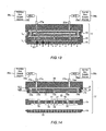
- Fig. 13 shows an enlarged diagram of the upper electrode 17 according to the second embodiment.
- same reference symbols are given to those portions which are the same as those in Fig. 2 and the description will be omitted.
- the plasma process system 1 has such a structure that a process gas and a carrier gas are diffused without contacting each other and are ejected from the gas holes 22. That is, as shown in Fig. 14. the upper electrode 17 is provided with a process gas supply tube 27a and a carrier gas supply tube 27b, which are respectively connected to the flow-rate control devices 29a and 29b and a process gas supply source 28a and a carrier gas supply source 28b.
- a mixture of various gases which have been used conventionally for deposition of an SiOF film such as SiF 4 , SiH 4 , O 2 , NF 3 and NH 3 , is supplied from the process gas supply source 28a and an Ar gas is supplied from the carrier gas supply source 28b.
- gas passages L c and L d are formed independently of each other and the process gas and carrier gas are diffused as they pass through the gas passage L c and L d , and are supplied approximately uniformly to the wafer W from the multiple gas holes 22 of the electrode plate 19.
- FIG. 14 An exploded diagram of the upper electrode 17 is shown in Fig. 14.
- the upper electrode 17 has such a structure that a disk-shaped diffusion plate 21 is sandwiched between the cylindrical electrode support 20 and the electrode plate 19.
- the two hollow portions 71 and 72 are laid out in such a way that their distances from the major surface of the electrode support 20 differ from each other.
- the first hollow portion 71 closer to the diffusion plate 21 is connected with seventh and eighth inlet ports 73a and 73b.
- the seventh inlet port 73a extends from the first hollow portion 71 in a direction perpendicular to the major surface of the electrode support 20 (the upper direction in the diagram) and communicates with the process gas supply tube 27a.
- the eighth inlet ports 73b extend from the first hollow portion 71 in the opposite direction (the lower direction in the diagram) to the seventh inlet port 73a and communicate with the bottom-side space of the electrode support 20. Accordingly, the process gas supplied from the process gas supply tube 27a flows through the gas passage L c which is constituted by the seventh inlet port 73a, the first hollow portion 71 and the eighth hollow portions 73b.
- the second hollow portion 72 formed farther from the diffusion plate 21 is connected with ninth and tenth inlet ports 74a and 74b.
- the ninth inlet port 74a extends from the second hollow portion 72 in a direction perpendicular to the major surface of the electrode support 20 (the upper direction in the diagram) and communicates with the carrier gas supply tube 27b.
- the tenth inlet ports 74b extend from the second hollow portion 72 in the opposite direction (the lower direction in the diagram) to the ninth inlet port 74a and communicate with the bottom-side space of the electrode support 20. Accordingly, the carrier gas supplied from the carrier gas supply tube 27b flows through the gas passage L d which is constituted by the ninth inlet port 74a, the second hollow portion 72 and the tenth hollow portions 74b.
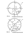
- Fig. 15 shows a cross-sectional view of the electrode support 20 shown in Fig. 14 as seen from an arrow A.
- the second hollow portion 72 comprises four first linear holes 72a, ..., 72a extending radially from approximately the center of the electrode support 20, and a second linear hole 72b provided radially from the same center between adjoining two first linear holes 72a.
- the first linear holes 72a, ..., 72a are provided in such a way as to be approximately orthogonal to one another.
- the first and second linear holes 72a and 72b are provided on approximately the same plane.
- the individual first linear holes 72a are connected to the tenth inlet ports 74b at points approximately equidistant from the center.
- the second linear hole 72b communicates with the ninth inlet port 74a.
- the carrier gas supplied from the carrier gas supply tube 27b passes the ninth inlet port 74a and flows to the second linear hole 72b.
- the carrier gas travels in the second linear hole 72b toward the center and is dispersed to the four first linear holes 72a from the center. Accordingly, the carrier gas is diffused horizontally.
- the carrier gas that has passed the first linear holes 72a flows toward the diffusion plate 21 from the tenth inlet ports 74b.
- the seventh inlet port 73a which connects to the process gas supply tube 27a is formed at such a position as not to overlap the second hollow portion 72.
- Fig. 16 shows a cross-sectional view of the upper electrode 17 shown in Fig. 14 as seen from an arrow B.
- the first hollow portion 71 comprises four third linear holes 71a, ..., 71a extending radially from approximately the center thereof, and a fourth linear hole 71b extending radially from the same center between adjoining two third linear holes 71a.
- the third linear holes 71a, ..., 71a are formed in approximately the same plane in such a way as to be nearly orthogonal to one another.
- the third and fourth linear holes 71a and 71b are provided at such a position as not to overlap the tenth inlet ports 74b.
- the individual third linear holes 71a are connected to the eighth inlet ports 73b at points approximately equidistant from the center and at the center.
- the fourth linear hole 71b communicates with the seventh inlet port 73a.
- the process gas supplied from the process gas supply tube 27a passes the seventh inlet port 73a and flows to the fourth linear hole 71b.
- the process gas travels in the fourth linear hole 71b toward the center and is dispersed to the four third linear holes 71a from the center.
- the process gas is diffused horizontally in this manner.
- the process gas that has passed the third linear holes 71a flows toward the diffusion plate 21 from the eighth inlet ports 73b.
- the linear holes 71a, 71b, 72a and 72b that constitute the first and second hollow portions 71 and 72 are formed by boring holes of a predetermined depth from the side wall of the electrode support 20 toward the center and sealing the end portions with sealing members 75.
- the linear holes are formed by boring holes in the side wall of the electrode support 20 from a approximately perpendicular direction toward the center thereof by a gun drill.
- the boring by the gun drill is performed plural times, for example, by turning the electrode support 20 around its center. Accordingly, a plurality of linear holes which communicate with one another at the center are formed. Thereafter, the end portions of the formed linear holes are sealed with the sealing members 75 made of the same material as the electrode support 20, thereby forming hollow portions.
- the first and second hollow portions 71 and 72 can be formed easily by changing, for example, the relative positions of the gun drill and the electrode support 20.
- the electrode support 20 with the above-described structure can be formed by forming holes (inlet ports) in the major surface of the electrode support 20 from the perpendicular direction in such a way as to reach the thus formed linear holes.
- a fourth channel 76 is formed in that side of the diffusion plate 21 which faces the electrode support 20.
- the fourth channel 76 is comprised of a plurality of grooves and forms a hollow portion with the bottom of the electrode support 20 covered.
- the fourth channel 76 is provided in such a way as to communicate the tenth inlet ports 74b but not to communicate eighth inlet ports 73b.
- Multiple first through ports 77 which penetrate the diffusion plate 21 are formed in the fourth channel 76 and are provided in such a way as to communicate with the gas holes 22, respectively.
- the fourth channel 76 and the first through ports 77 constitute the gas passage L d where the carrier gas flows.
- the carrier gas supplied to the diffusion plate 21 through the tenth inlet ports 74b is diffused horizontally by the fourth channel 76, passes through the first through ports 77 and is ejected from the multiple gas holes 22 approximately uniformly.
- Second through ports 78 are provided in the diffusion plate 21, penetrating it, in such a way as to communicate with the eighth inlet ports 73b.
- a fifth channel 79 is provided in that side of the diffusion plate 21 which faces the electrode plate 19.
- the fifth channel 79 is comprised of a plurality of grooves and forms a hollow portion with the top of the electrode plate 19 covered.
- the fifth channel 79 is provided in such a way as to communicate the second through ports 78 but not to communicate first through ports 77.
- the second through ports 78 and the fifth channel 79 constitute the gas passage L c where the process gas flows.
- the process gas supplied to the diffusion plate 21 through the eighth inlet ports 73b passes through the first through ports 77 and is diffused horizontally in the fifth channel 79.
- the fifth channel 79 communicates with the multiple gas holes 22, the diffused process gas is supplied from the gas holes 22 approximately uniformly.
- the multiple gas holes 22 in the diffusion plate 19 are connected to either the first through ports 77 or the fifth channel 79 in the same quantity, for example. Accordingly, the process gas which passes through the gas passage L c and the carrier gas which passes through the gas passage L d are diffused horizontally without contacting each other and are ejected through the gas holes 22 approximately uniformly. The process gas and the carrier gas are mixed inside the chamber 2 for the first time and are supplied onto the wafer W to be a plasma.
- the upper electrode 17 in the third embodiment has the following advantages. That is, the diffusion areas (first and second hollow portions 71 and 72) for diffusing a gas to be used in the process are formed by making holes in the electrode support 20 using a gun drill or the like. As the diffusion areas are formed inside the electrode support 20 this way, a process with high uniformity can be carried out with uniform gas supply from the gas holes 22 without increasing the number of parts or without complicating the system structure.
- the interface present in the upper electrode 17 e.g., the interface between the electrode support 20 and the diffusion plate 21
- the two independent gas passages L c and L d which do not communicate with each other are formed inside the upper electrode 17. If necessary, however, three gas passages or more may be provided in the upper electrode 17. In this case, for example, the number of hollow portions inside the electrode support 20 should be set to three layers of hollow portions or more by changing the distances from one side of the electrode support 20 respectively.
- the process gas is let to flow in the gas passage L c and the carrier gas is let to flow in the gas passage L d .
- gases which are not desirable to be mixed outside the chamber e.g., an inflammable and flame-aiding gas, may be let to flow in the gas passages L c and L d , respectively.
- each of the first and second hollow portions 71 and 72 in the electrode support 20 is comprised of four linear holes.
- the number of linear holes is not limited to this number but may be set to five or more for better diffusion of the gases.
- the method of forming the linear holes in the upper electrode 17 is not limited to boring by a gun drill, but boring may be performed by a laser or the like. Further, although the linear holes are formed with the depth from the side wall of the electrode support 20 to the center, they may be formed all the way through the electrode support 20.
- the upper electrode 17 is made of aluminum.
- the material for the upper electrode 17 is not limited to this material but conductive materials other than those which adversely influence the process, such as SUS, can be used as well.
- SiF 4 , SiH 4 , O 2 , NF 3 , NH 3 gases and an inactive gas, such as Ar or nitrogen, are used to deposit an SiOF film on a wafer in the first to third embodiments, the gases in use are not limited to them.
- a film to be deposited may be any film, such as an SiO 2 film, SiC film, SiN film, SiOC film or CF film.
- the invention is not limited to a system for a plasma CVD process but can be adapted to a system which performs a thermal CVD process, etc., as long as they supply a process gas from that side which faces the major surface of a subject to be processed via a shower-head type plate-like member and processes the to-be-processed subject, and can further be adapted to other systems which perform various processes, such as a deposition process, an etching process and a thermal process.
- the to-be-processed subject is not limited to a semiconductor wafer but may be a glass substrate or the like for a liquid crystal display device.
- the invention can be suitably used for fabrication of a process system which carries out a deposition process, an etching process, etc. on a subject to be processed, such as a semiconductor wafer.
Applications Claiming Priority (5)
| Application Number | Priority Date | Filing Date | Title |
|---|---|---|---|
| JP2001013570 | 2001-01-22 | ||
| JP2001013570 | 2001-01-22 | ||
| JP2001014011 | 2001-01-23 | ||
| JP2001014011 | 2001-01-23 | ||
| PCT/JP2002/000429 WO2002058126A1 (fr) | 2001-01-22 | 2002-01-22 | Dispositif et procede de traitement |
Publications (3)
| Publication Number | Publication Date |
|---|---|
| EP1361604A1 true EP1361604A1 (de) | 2003-11-12 |
| EP1361604A4 EP1361604A4 (de) | 2005-12-21 |
| EP1361604B1 EP1361604B1 (de) | 2009-03-18 |
Family
ID=26608083
Family Applications (1)
| Application Number | Title | Priority Date | Filing Date |
|---|---|---|---|
| EP02716335A Expired - Lifetime EP1361604B1 (de) | 2001-01-22 | 2002-01-22 | Einrichtung und verfahren zur behandlung |
Country Status (7)
| Country | Link |
|---|---|
| US (1) | US7481886B2 (de) |
| EP (1) | EP1361604B1 (de) |
| JP (1) | JP3946641B2 (de) |
| KR (1) | KR100516844B1 (de) |
| CN (1) | CN1328766C (de) |
| DE (1) | DE60231601D1 (de) |
| WO (1) | WO2002058126A1 (de) |
Cited By (2)
| Publication number | Priority date | Publication date | Assignee | Title |
|---|---|---|---|---|
| WO2008123391A2 (en) * | 2007-03-23 | 2008-10-16 | Panasonic Corporation | Apparatus and method for plasma doping |
| WO2008085474A3 (en) * | 2007-01-08 | 2008-11-06 | Eastman Kodak Co | Delivery device for thin film deposition |
Families Citing this family (85)
| Publication number | Priority date | Publication date | Assignee | Title |
|---|---|---|---|---|
| US8048806B2 (en) | 2000-03-17 | 2011-11-01 | Applied Materials, Inc. | Methods to avoid unstable plasma states during a process transition |
| US8617351B2 (en) * | 2002-07-09 | 2013-12-31 | Applied Materials, Inc. | Plasma reactor with minimal D.C. coils for cusp, solenoid and mirror fields for plasma uniformity and device damage reduction |
| US20070048882A1 (en) * | 2000-03-17 | 2007-03-01 | Applied Materials, Inc. | Method to reduce plasma-induced charging damage |
| US6502530B1 (en) * | 2000-04-26 | 2003-01-07 | Unaxis Balzers Aktiengesellschaft | Design of gas injection for the electrode in a capacitively coupled RF plasma reactor |
| WO2002058126A1 (fr) * | 2001-01-22 | 2002-07-25 | Tokyo Electron Limited | Dispositif et procede de traitement |
| JP4121269B2 (ja) * | 2001-11-27 | 2008-07-23 | 日本エー・エス・エム株式会社 | セルフクリーニングを実行するプラズマcvd装置及び方法 |
| JP4338355B2 (ja) * | 2002-05-10 | 2009-10-07 | 東京エレクトロン株式会社 | プラズマ処理装置 |
| TWI283899B (en) | 2002-07-09 | 2007-07-11 | Applied Materials Inc | Capacitively coupled plasma reactor with magnetic plasma control |
| US7169231B2 (en) * | 2002-12-13 | 2007-01-30 | Lam Research Corporation | Gas distribution system with tuning gas |
| JP3996502B2 (ja) * | 2002-12-27 | 2007-10-24 | 株式会社アルバック | 熱板表面のカバー機構を備えた処理装置 |
| US6844260B2 (en) * | 2003-01-30 | 2005-01-18 | Micron Technology, Inc. | Insitu post atomic layer deposition destruction of active species |
| KR100490049B1 (ko) * | 2003-04-14 | 2005-05-17 | 삼성전자주식회사 | 일체형 디퓨저 프레임을 가지는 cvd 장치 |
| JP4306403B2 (ja) * | 2003-10-23 | 2009-08-05 | 東京エレクトロン株式会社 | シャワーヘッド構造及びこれを用いた成膜装置 |
| US8317968B2 (en) * | 2004-04-30 | 2012-11-27 | Lam Research Corporation | Apparatus including gas distribution member supplying process gas and radio frequency (RF) power for plasma processing |
| CN102154628B (zh) * | 2004-08-02 | 2014-05-07 | 维高仪器股份有限公司 | 用于化学气相沉积反应器的多气体分配喷射器 |
| DE102005003984A1 (de) * | 2005-01-28 | 2006-08-03 | Aixtron Ag | Gaseinlassorgan für einen CVD-Reaktor |
| DE102005004312A1 (de) * | 2005-01-31 | 2006-08-03 | Aixtron Ag | Gasverteiler mit in Ebenen angeordneten Vorkammern |
| US7422636B2 (en) * | 2005-03-25 | 2008-09-09 | Tokyo Electron Limited | Plasma enhanced atomic layer deposition system having reduced contamination |
| KR101272321B1 (ko) * | 2005-05-09 | 2013-06-07 | 한국에이에스엠지니텍 주식회사 | 복수의 기체 유입구를 가지는 원자층 증착 장치의 반응기 |
| US20080081114A1 (en) * | 2006-10-03 | 2008-04-03 | Novellus Systems, Inc. | Apparatus and method for delivering uniform fluid flow in a chemical deposition system |
| KR101355638B1 (ko) * | 2006-11-09 | 2014-01-29 | 한국에이에스엠지니텍 주식회사 | 원자층 증착 장치 |
| US8702866B2 (en) * | 2006-12-18 | 2014-04-22 | Lam Research Corporation | Showerhead electrode assembly with gas flow modification for extended electrode life |
| US20080166880A1 (en) * | 2007-01-08 | 2008-07-10 | Levy David H | Delivery device for deposition |
| US11136667B2 (en) * | 2007-01-08 | 2021-10-05 | Eastman Kodak Company | Deposition system and method using a delivery head separated from a substrate by gas pressure |
| US20080236490A1 (en) * | 2007-03-29 | 2008-10-02 | Alexander Paterson | Plasma reactor with an overhead inductive antenna and an overhead gas distribution showerhead |
| KR101125086B1 (ko) * | 2007-04-17 | 2012-03-21 | 가부시키가이샤 알박 | 성막장치 |
| US8440259B2 (en) * | 2007-09-05 | 2013-05-14 | Intermolecular, Inc. | Vapor based combinatorial processing |
| US8211231B2 (en) * | 2007-09-26 | 2012-07-03 | Eastman Kodak Company | Delivery device for deposition |
| US8398770B2 (en) * | 2007-09-26 | 2013-03-19 | Eastman Kodak Company | Deposition system for thin film formation |
| US8673080B2 (en) | 2007-10-16 | 2014-03-18 | Novellus Systems, Inc. | Temperature controlled showerhead |
| JP5188782B2 (ja) * | 2007-11-13 | 2013-04-24 | 月島機械株式会社 | プラズマcvd装置及びプラスチック表面保護膜の形成方法 |
| US8628616B2 (en) | 2007-12-11 | 2014-01-14 | Sumitomo Electric Industries, Ltd. | Vapor-phase process apparatus, vapor-phase process method, and substrate |
| US8512509B2 (en) * | 2007-12-19 | 2013-08-20 | Applied Materials, Inc. | Plasma reactor gas distribution plate with radially distributed path splitting manifold |
| CN101488446B (zh) | 2008-01-14 | 2010-09-01 | 北京北方微电子基地设备工艺研究中心有限责任公司 | 等离子体处理设备及其气体分配装置 |
| US7879183B2 (en) * | 2008-02-27 | 2011-02-01 | Applied Materials, Inc. | Apparatus and method for front side protection during backside cleaning |
| JP5223377B2 (ja) * | 2008-02-29 | 2013-06-26 | 東京エレクトロン株式会社 | プラズマ処理装置用の電極、プラズマ処理装置及びプラズマ処理方法 |
| JP5179389B2 (ja) * | 2008-03-19 | 2013-04-10 | 東京エレクトロン株式会社 | シャワーヘッド及び基板処理装置 |
| JP5075793B2 (ja) * | 2008-11-06 | 2012-11-21 | 東京エレクトロン株式会社 | 可動ガス導入構造物及び基板処理装置 |
| US8293013B2 (en) * | 2008-12-30 | 2012-10-23 | Intermolecular, Inc. | Dual path gas distribution device |
| CN102460635B (zh) * | 2009-05-06 | 2014-12-24 | 3M创新有限公司 | 对容器进行等离子体处理的装置和方法 |
| KR101559470B1 (ko) | 2009-06-04 | 2015-10-12 | 주성엔지니어링(주) | 화학 기상 증착 장치 |
| KR101110080B1 (ko) * | 2009-07-08 | 2012-03-13 | 주식회사 유진테크 | 확산판을 선택적으로 삽입설치하는 기판처리방법 |
| TWI430714B (zh) * | 2009-10-15 | 2014-03-11 | Orbotech Lt Solar Llc | 電漿處理腔之噴撒頭組件及電漿處理腔之噴撒頭組件之氣體電離板之製備方法 |
| US20110097489A1 (en) * | 2009-10-27 | 2011-04-28 | Kerr Roger S | Distribution manifold including multiple fluid communication ports |
| TWI436831B (zh) | 2009-12-10 | 2014-05-11 | Orbotech Lt Solar Llc | 真空處理裝置之噴灑頭總成 |
| CN102234791B (zh) * | 2010-05-05 | 2014-02-12 | 财团法人工业技术研究院 | 气体分布喷洒模块与镀膜设备 |
| JP5567392B2 (ja) * | 2010-05-25 | 2014-08-06 | 東京エレクトロン株式会社 | プラズマ処理装置 |
| KR101430744B1 (ko) * | 2010-06-21 | 2014-08-18 | 세메스 주식회사 | 박막 증착 장치 |
| US9184028B2 (en) | 2010-08-04 | 2015-11-10 | Lam Research Corporation | Dual plasma volume processing apparatus for neutral/ion flux control |
| US8869742B2 (en) * | 2010-08-04 | 2014-10-28 | Lam Research Corporation | Plasma processing chamber with dual axial gas injection and exhaust |
| US8470614B2 (en) * | 2010-10-28 | 2013-06-25 | Texas Instruments Incorporated | PECVD showerhead configuration for CMP uniformity and improved stress |
| WO2012122054A2 (en) | 2011-03-04 | 2012-09-13 | Novellus Systems, Inc. | Hybrid ceramic showerhead |
| US8459276B2 (en) | 2011-05-24 | 2013-06-11 | Orbotech LT Solar, LLC. | Broken wafer recovery system |
| JP5898549B2 (ja) | 2012-03-29 | 2016-04-06 | 株式会社Screenホールディングス | 基板処理方法および基板処理装置 |
| JP6157061B2 (ja) | 2012-05-11 | 2017-07-05 | 東京エレクトロン株式会社 | ガス供給装置及び基板処理装置 |
| JP2014082354A (ja) * | 2012-10-17 | 2014-05-08 | Hitachi High-Technologies Corp | プラズマ処理装置 |
| DE102013101534A1 (de) | 2013-02-15 | 2014-08-21 | Aixtron Se | Gasverteiler für einen CVD-Reaktor |
| KR102130061B1 (ko) * | 2013-03-15 | 2020-07-03 | 어플라이드 머티어리얼스, 인코포레이티드 | 매우 대칭적인 4-폴드 가스 주입부를 갖는 플라즈마 반응기 |
| JP6007143B2 (ja) * | 2013-03-26 | 2016-10-12 | 東京エレクトロン株式会社 | シャワーヘッド、プラズマ処理装置、及びプラズマ処理方法 |
| US9353439B2 (en) | 2013-04-05 | 2016-05-31 | Lam Research Corporation | Cascade design showerhead for transient uniformity |
| CN103305923B (zh) * | 2013-06-06 | 2017-05-10 | 北京七星华创电子股份有限公司 | 一种热处理反应管构件 |
| CN203890438U (zh) * | 2013-06-08 | 2014-10-22 | 唐治 | 一种用于碳化硅外延生长的化学气相沉积装置 |
| JP6210792B2 (ja) * | 2013-08-13 | 2017-10-11 | 株式会社ディスコ | プラズマエッチング装置 |
| KR20150046966A (ko) * | 2013-10-23 | 2015-05-04 | 삼성디스플레이 주식회사 | 플라즈마 처리 장치 및 플라즈마 처리 방법 |
| JP6406811B2 (ja) * | 2013-11-20 | 2018-10-17 | 国立大学法人名古屋大学 | Iii 族窒化物半導体装置の製造装置および製造方法ならびに半導体ウエハの製造方法 |
| KR101455734B1 (ko) * | 2014-04-14 | 2014-11-05 | 세메스 주식회사 | 박막 증착 장치 |
| US10741365B2 (en) * | 2014-05-05 | 2020-08-11 | Lam Research Corporation | Low volume showerhead with porous baffle |
| JP6169040B2 (ja) * | 2014-05-12 | 2017-07-26 | 東京エレクトロン株式会社 | プラズマ処理装置の上部電極構造、プラズマ処理装置、及びプラズマ処理装置の運用方法 |
| SG11201608640QA (en) * | 2014-05-16 | 2016-11-29 | Applied Materials Inc | Showerhead design |
| JP5837962B1 (ja) * | 2014-07-08 | 2015-12-24 | 株式会社日立国際電気 | 基板処理装置、半導体装置の製造方法およびガス整流部 |
| US9228260B1 (en) * | 2014-07-30 | 2016-01-05 | Taiwan Semiconductor Manufacturing Co., Ltd. | Wafer processing chamber, heat treatment apparatus and method for processing wafers |
| KR102267923B1 (ko) | 2014-08-26 | 2021-06-22 | 에이에스엠 아이피 홀딩 비.브이. | 증착 장치 |
| US10378107B2 (en) | 2015-05-22 | 2019-08-13 | Lam Research Corporation | Low volume showerhead with faceplate holes for improved flow uniformity |
| US10023959B2 (en) | 2015-05-26 | 2018-07-17 | Lam Research Corporation | Anti-transient showerhead |
| TWI723024B (zh) | 2015-06-26 | 2021-04-01 | 美商應用材料股份有限公司 | 用於改良的氣體分配的遞迴注入設備 |
| US10829855B2 (en) * | 2016-05-20 | 2020-11-10 | Applied Materials, Inc. | Gas distribution showerhead for semiconductor processing |
| JP6495875B2 (ja) | 2016-09-12 | 2019-04-03 | 株式会社東芝 | 流路構造及び処理装置 |
| US10851457B2 (en) | 2017-08-31 | 2020-12-01 | Lam Research Corporation | PECVD deposition system for deposition on selective side of the substrate |
| KR102636427B1 (ko) * | 2018-02-20 | 2024-02-13 | 에이에스엠 아이피 홀딩 비.브이. | 기판 처리 방법 및 장치 |
| KR20230156441A (ko) | 2019-08-16 | 2023-11-14 | 램 리써치 코포레이션 | 웨이퍼 내에서 차동 보우를 보상하기 위한 공간적으로 튜닝 가능한 증착 |
| CN111321463B (zh) * | 2020-03-06 | 2021-10-15 | 北京北方华创微电子装备有限公司 | 反应腔室 |
| TW202147492A (zh) * | 2020-06-03 | 2021-12-16 | 荷蘭商Asm Ip私人控股有限公司 | 噴淋板、基板處理裝置、基板處理方法 |
| US20220028710A1 (en) * | 2020-07-21 | 2022-01-27 | Applied Materials, Inc. | Distribution components for semiconductor processing systems |
| KR20220086716A (ko) * | 2020-12-03 | 2022-06-23 | 램 리써치 코포레이션 | 웨이퍼 보우 (bow) 보상을 위한 배면 증착 및 국부 응력 조절 |
| US20220350251A1 (en) * | 2021-05-03 | 2022-11-03 | Applied Materials, Inc. | Chamber and methods of treating a substrate after exposure to radiation |
Citations (7)
| Publication number | Priority date | Publication date | Assignee | Title |
|---|---|---|---|---|
| US5595606A (en) * | 1995-04-20 | 1997-01-21 | Tokyo Electron Limited | Shower head and film forming apparatus using the same |
| US6086677A (en) * | 1998-06-16 | 2000-07-11 | Applied Materials, Inc. | Dual gas faceplate for a showerhead in a semiconductor wafer processing system |
| US6148761A (en) * | 1998-06-16 | 2000-11-21 | Applied Materials, Inc. | Dual channel gas distribution plate |
| WO2001003159A1 (en) * | 1999-06-30 | 2001-01-11 | Lam Research Corporation | Gas distribution apparatus for semiconductor processing |
| WO2001061071A2 (de) * | 2000-02-16 | 2001-08-23 | Aixtron Ag | Kondensationsbeschichtungsverfahren |
| EP1134789A2 (de) * | 2000-03-16 | 2001-09-19 | Applied Materials, Inc. | Einteilige Doppelgas-Frontplatte für einen Verteilungskopf in einem Verarbeitungssystem für Halbleiterwafer |
| WO2002023964A1 (en) * | 2000-09-13 | 2002-03-21 | Applied Materials, Inc. | Processing chamber with multi-layer brazed lid |
Family Cites Families (38)
| Publication number | Priority date | Publication date | Assignee | Title |
|---|---|---|---|---|
| US4590042A (en) * | 1984-12-24 | 1986-05-20 | Tegal Corporation | Plasma reactor having slotted manifold |
| US4820371A (en) * | 1987-12-15 | 1989-04-11 | Texas Instruments Incorporated | Apertured ring for exhausting plasma reactor gases |
| JP3081003B2 (ja) * | 1991-01-22 | 2000-08-28 | アネルバ株式会社 | プラズマ処理装置 |
| US5266153A (en) * | 1992-06-16 | 1993-11-30 | National Semiconductor Corp. | Gas distribution head for plasma deposition and etch systems |
| US5558717A (en) * | 1994-11-30 | 1996-09-24 | Applied Materials | CVD Processing chamber |
| JPH0945624A (ja) * | 1995-07-27 | 1997-02-14 | Tokyo Electron Ltd | 枚葉式の熱処理装置 |
| JP3360265B2 (ja) * | 1996-04-26 | 2002-12-24 | 東京エレクトロン株式会社 | プラズマ処理方法及びプラズマ処理装置 |
| US6294026B1 (en) * | 1996-11-26 | 2001-09-25 | Siemens Aktiengesellschaft | Distribution plate for a reaction chamber with multiple gas inlets and separate mass flow control loops |
| JP3341619B2 (ja) * | 1997-03-04 | 2002-11-05 | 東京エレクトロン株式会社 | 成膜装置 |
| JPH1154496A (ja) * | 1997-08-07 | 1999-02-26 | Tokyo Electron Ltd | 熱処理装置及びガス処理装置 |
| US6161500A (en) * | 1997-09-30 | 2000-12-19 | Tokyo Electron Limited | Apparatus and method for preventing the premature mixture of reactant gases in CVD and PECVD reactions |
| KR100505310B1 (ko) * | 1998-05-13 | 2005-08-04 | 동경 엘렉트론 주식회사 | 성막 장치 및 방법 |
| JP2000058299A (ja) * | 1998-08-07 | 2000-02-25 | Matsushita Electric Ind Co Ltd | 電極取り付け方法およびプラズマ処理装置ならびにスパッタリング装置 |
| US6190732B1 (en) * | 1998-09-03 | 2001-02-20 | Cvc Products, Inc. | Method and system for dispensing process gas for fabricating a device on a substrate |
| US6415736B1 (en) * | 1999-06-30 | 2002-07-09 | Lam Research Corporation | Gas distribution apparatus for semiconductor processing |
| US6123775A (en) * | 1999-06-30 | 2000-09-26 | Lam Research Corporation | Reaction chamber component having improved temperature uniformity |
| US6206972B1 (en) * | 1999-07-08 | 2001-03-27 | Genus, Inc. | Method and apparatus for providing uniform gas delivery to substrates in CVD and PECVD processes |
| JP4487338B2 (ja) * | 1999-08-31 | 2010-06-23 | 東京エレクトロン株式会社 | 成膜処理装置及び成膜処理方法 |
| TW484189B (en) * | 1999-11-17 | 2002-04-21 | Tokyo Electron Ltd | Precoat film forming method, idling method of film forming device, loading table structure, film forming device and film forming method |
| JP3645768B2 (ja) * | 1999-12-07 | 2005-05-11 | シャープ株式会社 | プラズマプロセス装置 |
| KR20010062209A (ko) * | 1999-12-10 | 2001-07-07 | 히가시 데쓰로 | 고내식성 막이 내부에 형성된 챔버를 구비하는 처리 장치 |
| US6444039B1 (en) * | 2000-03-07 | 2002-09-03 | Simplus Systems Corporation | Three-dimensional showerhead apparatus |
| US6502530B1 (en) * | 2000-04-26 | 2003-01-07 | Unaxis Balzers Aktiengesellschaft | Design of gas injection for the electrode in a capacitively coupled RF plasma reactor |
| US6537419B1 (en) * | 2000-04-26 | 2003-03-25 | David W. Kinnard | Gas distribution plate assembly for providing laminar gas flow across the surface of a substrate |
| KR100406174B1 (ko) * | 2000-06-15 | 2003-11-19 | 주식회사 하이닉스반도체 | 화학적 강화 화학 기상 증착 장비에 사용되는 샤워 헤드 |
| JP3578398B2 (ja) * | 2000-06-22 | 2004-10-20 | 古河スカイ株式会社 | 成膜用ガス分散プレート及びその製造方法 |
| AU2002241496A1 (en) * | 2000-11-20 | 2002-06-18 | Applied Epi, Inc. | Surface sealing showerhead for vapor deposition reactor having integrated flow diverters |
| WO2002058126A1 (fr) * | 2001-01-22 | 2002-07-25 | Tokyo Electron Limited | Dispositif et procede de traitement |
| KR100691758B1 (ko) * | 2001-03-16 | 2007-03-12 | 동경 엘렉트론 주식회사 | 박막 형성 방법 및 박막 형성 장치 |
| KR100702002B1 (ko) * | 2001-06-25 | 2007-03-30 | 삼성전자주식회사 | 반도체 웨이퍼 처리 장치용 샤워헤드 |
| KR100400044B1 (ko) * | 2001-07-16 | 2003-09-29 | 삼성전자주식회사 | 간격 조절 장치를 가지는 웨이퍼 처리 장치의 샤워 헤드 |
| US20030124842A1 (en) * | 2001-12-27 | 2003-07-03 | Applied Materials, Inc. | Dual-gas delivery system for chemical vapor deposition processes |
| US6866746B2 (en) * | 2002-01-26 | 2005-03-15 | Applied Materials, Inc. | Clamshell and small volume chamber with fixed substrate support |
| US7524532B2 (en) * | 2002-04-22 | 2009-04-28 | Aixtron Ag | Process for depositing thin layers on a substrate in a process chamber of adjustable height |
| AU2003282533A1 (en) * | 2002-08-08 | 2004-02-25 | Trikon Technologies Limited | Improvements to showerheads |
| TW587139B (en) * | 2002-10-18 | 2004-05-11 | Winbond Electronics Corp | Gas distribution system and method for the plasma gas in the chamber |
| US20040112540A1 (en) * | 2002-12-13 | 2004-06-17 | Lam Research Corporation | Uniform etch system |
| US20050011447A1 (en) * | 2003-07-14 | 2005-01-20 | Tokyo Electron Limited | Method and apparatus for delivering process gas to a process chamber |
-
2002
- 2002-01-22 WO PCT/JP2002/000429 patent/WO2002058126A1/ja active IP Right Grant
- 2002-01-22 KR KR10-2003-7009599A patent/KR100516844B1/ko not_active IP Right Cessation
- 2002-01-22 CN CNB028039165A patent/CN1328766C/zh not_active Expired - Fee Related
- 2002-01-22 JP JP2002558318A patent/JP3946641B2/ja not_active Expired - Fee Related
- 2002-01-22 EP EP02716335A patent/EP1361604B1/de not_active Expired - Lifetime
- 2002-01-22 DE DE60231601T patent/DE60231601D1/de not_active Expired - Lifetime
-
2003
- 2003-07-22 US US10/623,866 patent/US7481886B2/en not_active Expired - Fee Related
Patent Citations (7)
| Publication number | Priority date | Publication date | Assignee | Title |
|---|---|---|---|---|
| US5595606A (en) * | 1995-04-20 | 1997-01-21 | Tokyo Electron Limited | Shower head and film forming apparatus using the same |
| US6086677A (en) * | 1998-06-16 | 2000-07-11 | Applied Materials, Inc. | Dual gas faceplate for a showerhead in a semiconductor wafer processing system |
| US6148761A (en) * | 1998-06-16 | 2000-11-21 | Applied Materials, Inc. | Dual channel gas distribution plate |
| WO2001003159A1 (en) * | 1999-06-30 | 2001-01-11 | Lam Research Corporation | Gas distribution apparatus for semiconductor processing |
| WO2001061071A2 (de) * | 2000-02-16 | 2001-08-23 | Aixtron Ag | Kondensationsbeschichtungsverfahren |
| EP1134789A2 (de) * | 2000-03-16 | 2001-09-19 | Applied Materials, Inc. | Einteilige Doppelgas-Frontplatte für einen Verteilungskopf in einem Verarbeitungssystem für Halbleiterwafer |
| WO2002023964A1 (en) * | 2000-09-13 | 2002-03-21 | Applied Materials, Inc. | Processing chamber with multi-layer brazed lid |
Non-Patent Citations (1)
| Title |
|---|
| See also references of WO02058126A1 * |
Cited By (4)
| Publication number | Priority date | Publication date | Assignee | Title |
|---|---|---|---|---|
| WO2008085474A3 (en) * | 2007-01-08 | 2008-11-06 | Eastman Kodak Co | Delivery device for thin film deposition |
| US7789961B2 (en) | 2007-01-08 | 2010-09-07 | Eastman Kodak Company | Delivery device comprising gas diffuser for thin film deposition |
| WO2008123391A2 (en) * | 2007-03-23 | 2008-10-16 | Panasonic Corporation | Apparatus and method for plasma doping |
| WO2008123391A3 (en) * | 2007-03-23 | 2009-01-15 | Panasonic Corp | Apparatus and method for plasma doping |
Also Published As
| Publication number | Publication date |
|---|---|
| WO2002058126A1 (fr) | 2002-07-25 |
| DE60231601D1 (de) | 2009-04-30 |
| JPWO2002058126A1 (ja) | 2004-09-30 |
| KR100516844B1 (ko) | 2005-09-26 |
| CN1582488A (zh) | 2005-02-16 |
| US7481886B2 (en) | 2009-01-27 |
| CN1328766C (zh) | 2007-07-25 |
| US20040134611A1 (en) | 2004-07-15 |
| KR20030071836A (ko) | 2003-09-06 |
| EP1361604A4 (de) | 2005-12-21 |
| EP1361604B1 (de) | 2009-03-18 |
| JP3946641B2 (ja) | 2007-07-18 |
Similar Documents
| Publication | Publication Date | Title |
|---|---|---|
| EP1361604B1 (de) | Einrichtung und verfahren zur behandlung | |
| JP4454621B2 (ja) | 処理装置 | |
| CN101065513B (zh) | 用于改良瞬时相沉积的气体分配系统 | |
| KR100743792B1 (ko) | 증착 챔버 내에서 기판 상에 박막을 증착하는 방법 | |
| KR102588544B1 (ko) | 가스 분배 및 개별적인 펌핑을 갖는 배치 경화 챔버 | |
| US20030019428A1 (en) | Chemical vapor deposition chamber | |
| US20030119328A1 (en) | Plasma processing apparatus, and cleaning method therefor | |
| US7074461B2 (en) | Method for fabricating hydrogenated silicon oxycarbide thin film | |
| US20160322200A1 (en) | Dual-channel showerhead for formation of film stacks | |
| EP1168427A1 (de) | Verfahren zur Plasma-Abscheidung von Silizium-Nitrid | |
| TWI803753B (zh) | 具有背側泵送的熱處理腔室蓋 | |
| TWI827877B (zh) | 化學氣相沉積設備、泵浦襯套及化學氣相沉積方法 | |
| US20210032753A1 (en) | Methods and apparatus for dual channel showerheads | |
| KR20210158823A (ko) | 공정 도구를 위한 샤워헤드 | |
| KR102210390B1 (ko) | 유동가능한 cvd를 위한 이중 원격 플라즈마 소스들의 통합 | |
| US20180258531A1 (en) | Diffuser design for flowable cvd | |
| TW201833361A (zh) | 薄膜封裝處理系統和處理套組 | |
| KR20030002776A (ko) | 박막 증착 장비 | |
| KR102538276B1 (ko) | Pe-cvd 장치 및 방법 | |
| TWI813375B (zh) | 具有氣體分佈及個別泵送的批次固化腔室 | |
| TW202139324A (zh) | 用以管理不均勻性的晶圓平面下方之非對稱沖洗塊 |
Legal Events
| Date | Code | Title | Description |
|---|---|---|---|
| PUAI | Public reference made under article 153(3) epc to a published international application that has entered the european phase |
Free format text: ORIGINAL CODE: 0009012 |
|
| 17P | Request for examination filed |
Effective date: 20030722 |
|
| AK | Designated contracting states |
Kind code of ref document: A1 Designated state(s): AT BE CH CY DE DK ES FI FR GB GR IE IT LI LU MC NL PT SE TR |
|
| AX | Request for extension of the european patent |
Extension state: AL LT LV MK RO SI |
|
| A4 | Supplementary search report drawn up and despatched |
Effective date: 20051107 |
|
| RIC1 | Information provided on ipc code assigned before grant |
Ipc: 7H 01J 37/32 B Ipc: 7C 23C 16/455 A |
|
| 17Q | First examination report despatched |
Effective date: 20070301 |
|
| GRAP | Despatch of communication of intention to grant a patent |
Free format text: ORIGINAL CODE: EPIDOSNIGR1 |
|
| RBV | Designated contracting states (corrected) |
Designated state(s): DE FR GB IT |
|
| GRAS | Grant fee paid |
Free format text: ORIGINAL CODE: EPIDOSNIGR3 |
|
| GRAA | (expected) grant |
Free format text: ORIGINAL CODE: 0009210 |
|
| AK | Designated contracting states |
Kind code of ref document: B1 Designated state(s): DE FR GB IT |
|
| REG | Reference to a national code |
Ref country code: GB Ref legal event code: FG4D |
|
| REF | Corresponds to: |
Ref document number: 60231601 Country of ref document: DE Date of ref document: 20090430 Kind code of ref document: P |
|
| PLBE | No opposition filed within time limit |
Free format text: ORIGINAL CODE: 0009261 |
|
| STAA | Information on the status of an ep patent application or granted ep patent |
Free format text: STATUS: NO OPPOSITION FILED WITHIN TIME LIMIT |
|
| 26N | No opposition filed |
Effective date: 20091221 |
|
| GBPC | Gb: european patent ceased through non-payment of renewal fee |
Effective date: 20100122 |
|
| REG | Reference to a national code |
Ref country code: FR Ref legal event code: ST Effective date: 20100930 |
|
| PG25 | Lapsed in a contracting state [announced via postgrant information from national office to epo] |
Ref country code: FR Free format text: LAPSE BECAUSE OF NON-PAYMENT OF DUE FEES Effective date: 20100201 |
|
| PG25 | Lapsed in a contracting state [announced via postgrant information from national office to epo] |
Ref country code: GB Free format text: LAPSE BECAUSE OF NON-PAYMENT OF DUE FEES Effective date: 20100122 |
|
| PG25 | Lapsed in a contracting state [announced via postgrant information from national office to epo] |
Ref country code: IT Free format text: LAPSE BECAUSE OF FAILURE TO SUBMIT A TRANSLATION OF THE DESCRIPTION OR TO PAY THE FEE WITHIN THE PRESCRIBED TIME-LIMIT Effective date: 20090318 |
|
| PGFP | Annual fee paid to national office [announced via postgrant information from national office to epo] |
Ref country code: DE Payment date: 20150113 Year of fee payment: 14 |
|
| REG | Reference to a national code |
Ref country code: DE Ref legal event code: R119 Ref document number: 60231601 Country of ref document: DE |
|
| PG25 | Lapsed in a contracting state [announced via postgrant information from national office to epo] |
Ref country code: DE Free format text: LAPSE BECAUSE OF NON-PAYMENT OF DUE FEES Effective date: 20160802 |