EP1349171B1 - Data-Austauschvorrichtung zwischen Abtastketten - Google Patents
Data-Austauschvorrichtung zwischen Abtastketten Download PDFInfo
- Publication number
- EP1349171B1 EP1349171B1 EP03251315A EP03251315A EP1349171B1 EP 1349171 B1 EP1349171 B1 EP 1349171B1 EP 03251315 A EP03251315 A EP 03251315A EP 03251315 A EP03251315 A EP 03251315A EP 1349171 B1 EP1349171 B1 EP 1349171B1
- Authority
- EP
- European Patent Office
- Prior art keywords
- pair
- data
- scan
- scan chains
- register
- Prior art date
- Legal status (The legal status is an assumption and is not a legal conclusion. Google has not performed a legal analysis and makes no representation as to the accuracy of the status listed.)
- Expired - Lifetime
Links
- 230000003068 static effect Effects 0.000 claims description 4
- 238000003491 array Methods 0.000 description 11
- 238000000034 method Methods 0.000 description 10
- 230000008569 process Effects 0.000 description 5
- 230000006870 function Effects 0.000 description 4
- 230000005415 magnetization Effects 0.000 description 4
- 238000013500 data storage Methods 0.000 description 3
- 239000000696 magnetic material Substances 0.000 description 3
- 230000008878 coupling Effects 0.000 description 2
- 238000010168 coupling process Methods 0.000 description 2
- 238000005859 coupling reaction Methods 0.000 description 2
- 241000042032 Petrocephalus catostoma Species 0.000 description 1
- 230000008859 change Effects 0.000 description 1
- 230000001419 dependent effect Effects 0.000 description 1
- 230000009977 dual effect Effects 0.000 description 1
- 230000000694 effects Effects 0.000 description 1
- 238000005516 engineering process Methods 0.000 description 1
- 230000007774 longterm Effects 0.000 description 1
- 239000000463 material Substances 0.000 description 1
- 230000004048 modification Effects 0.000 description 1
- 238000012986 modification Methods 0.000 description 1
- 230000001360 synchronised effect Effects 0.000 description 1
Images


Classifications
-
- G—PHYSICS
- G11—INFORMATION STORAGE
- G11C—STATIC STORES
- G11C7/00—Arrangements for writing information into, or reading information out from, a digital store
-
- G—PHYSICS
- G11—INFORMATION STORAGE
- G11C—STATIC STORES
- G11C29/00—Checking stores for correct operation ; Subsequent repair; Testing stores during standby or offline operation
- G11C29/04—Detection or location of defective memory elements, e.g. cell constructio details, timing of test signals
- G11C29/08—Functional testing, e.g. testing during refresh, power-on self testing [POST] or distributed testing
- G11C29/48—Arrangements in static stores specially adapted for testing by means external to the store, e.g. using direct memory access [DMA] or using auxiliary access paths
-
- G—PHYSICS
- G11—INFORMATION STORAGE
- G11C—STATIC STORES
- G11C11/00—Digital stores characterised by the use of particular electric or magnetic storage elements; Storage elements therefor
- G11C11/02—Digital stores characterised by the use of particular electric or magnetic storage elements; Storage elements therefor using magnetic elements
- G11C11/16—Digital stores characterised by the use of particular electric or magnetic storage elements; Storage elements therefor using magnetic elements using elements in which the storage effect is based on magnetic spin effect
-
- G—PHYSICS
- G11—INFORMATION STORAGE
- G11C—STATIC STORES
- G11C19/00—Digital stores in which the information is moved stepwise, e.g. shift registers
-
- G—PHYSICS
- G11—INFORMATION STORAGE
- G11C—STATIC STORES
- G11C7/00—Arrangements for writing information into, or reading information out from, a digital store
- G11C7/10—Input/output [I/O] data interface arrangements, e.g. I/O data control circuits, I/O data buffers
- G11C7/1051—Data output circuits, e.g. read-out amplifiers, data output buffers, data output registers, data output level conversion circuits
-
- G—PHYSICS
- G11—INFORMATION STORAGE
- G11C—STATIC STORES
- G11C7/00—Arrangements for writing information into, or reading information out from, a digital store
- G11C7/10—Input/output [I/O] data interface arrangements, e.g. I/O data control circuits, I/O data buffers
- G11C7/1078—Data input circuits, e.g. write amplifiers, data input buffers, data input registers, data input level conversion circuits
-
- G—PHYSICS
- G11—INFORMATION STORAGE
- G11C—STATIC STORES
- G11C2207/00—Indexing scheme relating to arrangements for writing information into, or reading information out from, a digital store
- G11C2207/10—Aspects relating to interfaces of memory device to external buses
- G11C2207/107—Serial-parallel conversion of data or prefetch
Definitions
- the present invention relates to devices for data storage and retrieval, for example, memory apparatus which may be of resistive cross point memory (RXPtM) cell type (one example of which is a magnetic random access memory (MRAM)), having multiple serial data and control paths.
- the multiple serial data paths may be merged and may exchange data as needed by the data input/output (1/0) circuits connected to a serial I/O port.
- a plurality of scan path registers may be connected by an array of static random access memory (SRAM) memory cells to perform a parallel transfer of data from scan path registers to and from temporary registers in the SRAM memory array in order to effect data exchange between the multiple scan path registers.
- SRAM static random access memory
- a scan chain is a set of registers connected in series with a facility to shift data between the registers in the series, in order to transfer data from the one end of the scan chain to the other or to perform the function of controlling the state of the registers of the scan chain, for example.
- An example of the use of a scan chain is to connect the I/O pads of a chip as a facility to serially transfer control data and address data applied to the input of the chip to the memory control blocks or the memory array blocks and to serially transfer output data from the memory array or control blocks to the I/O pads of the chip.
- a serial scan chain commonly found in digital integrated circuits is a "boundary scan chain" in which the I/O for a chip or circuit block is connected to a scan chain to provide the option to extract the I/O in parallel or to extract the I/O in a serial manner by shifting the I/O to a single output port through the "boundary scan chain.”
- boundary scan chain connects the parallel control and I/O functions of a system block to a small set of serial data ports.
- Scan chains may also be found in digital logic systems connecting all the registers of the system together as part of a scan test system.
- One example of a system that may contain many control and data scan chains is an MRAM memory.
- MRAM memory Such an MRAM memory would be a complete device, including system controls, with multiple local data I/O scan chains connecting together sub-blocks of the MRAM memory cell arrays, and a scan chain to connect the system I/O ports.
- United States patent number 5,719,504 (Yamada) is believed to describe a register (flip-flop) found in combinational logic that may be serially connected in a scan chain for the purpose of storing the state of the registers and allowing the contents of the registers to be shifted in and out of the circuit using a scan chain.
- United States patent number 5,953,285 (Churchill) is believed to describe a control register as an interface to a memory circuit and features synchronous or asynchronous modes of operation where the register may contain a scan register.
- United States patent number 5,867,507 discloses memory cells interconnecting different scan chains and used in transferring the data from one scan chain to another.
- Magnetic Random Access Memory is a non-volatile memory that is being considered for long term data storage.
- a typical MRAM device includes an array of memory cells. Word lines extend along rows of the memory cells, and bit lines extend along columns of the memory cells. The memory cells are each located at a cross point of a word line and a bit line, and each memory cell includes two masses of magnetic material. One of the masses is magnetically fixed and the other is magnetically variable. A memory cell stores a bit of information as the orientation of relative magnetization of the fixed and variable materials. In other words, the magnetisation of each memory cell at any given time assumes one of two stable orientations. These two stable orientations.
- parallel and anti-parallel magnetic orientation represent logic values of '0' and '1,' for example.
- the resistance of a memory cell varies dependent upon whether it stores a "0" or a "1" value. That is, the resistance of a memory cell is a first value "R” if the orientation of the magnetization of the fixed magnetic material and of the variable magnetic material is parallel, and the resistance of the memory cell is increased to a second value R+DR if the orientation of the magnetization is anti-parallel.
- the orientation of the relative magnetization of a selected memory cell may be sensed by sensing the resistance value of the selected memory cell.
- an implementation of this invention may utilize MRAM memory. That is, an example of this invention may be implemented in an MRAM memory device, which memory device has control and data scan chains, as mentioned above.
- the present invention seeks to provide an improved data exchange device and method.
- the preferred embodiment can provide an effective and efficient solution for coupling multiple scan chains with the possibility of adding varying amounts of extra storage memory for exchanging data between the scan chains by providing a SRAM memory array at the junction of the multiple scan chains.
- multiple scan chain registers are combined with an SRAM memory to perform a parallel transfer of data from scan path registers to temporary storage in the SRAM memory and to another of the plural scan chain registers in a process to exchange data between the multiple scan chain registers.
- MRAM memory sub-arrays have an access time interval that is sufficiently long that relatively long data scan chains can be parallel loaded during a memory sub-array access interval. By accessing a large number of sub-arrays in parallel, a higher level of data transfer performance may be achieved in such a memory device.
- the present application discloses a register-based circuit for exchanging data between several scan chains, at least one of which may interface with the I/O circuits for outputting data.
- the present invention also provides a method of exchanging data among plural scan chains.
- the scan chains may be static during the data exchange, but more preferably are dynamic during the data exchange.
- Embodiments of the present invention provide for dynamic operation of the scan chains even while data is exchanged and shared among the plural scan chains.
- the present invention provides a method and apparatus for exchanging data between multiple scan chains.
- One example of an implementation of this invention is an SRAM memory device, which includes the I/O data paths from a group of MRAM memory arrays, a set of SRAM registers, and in input/output (I/O) controller.
- I/O input/output
- other types of devices and other types of memory besides SRAM may be implemented according to the present invention.
- system and method allow multiple serial data paths to merge and to exchange data as needed by the data input/output I/O port.
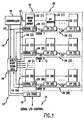
- a MRAM memory device 10 is very generally depicted.
- This device may be considered to have a "size" indicated by the arbitrary numbers NxM, in which N and M are respectively indicative of the number of MRAM sub-arrays in a row of the device, and the number of such rows of MRAM sub-arrays, as will be further explained below. That is, the device 10 illustrated in Figure 1 is of indeterminate size, and devices of various sizes may be implemented by the invention. The invention is not limited to the implementation of memory devices of any particular size. Nor is the invention limited to the implementation of a memory device.
- This particular exemplary MRAM device 10 includes an array of contact pads 12, generally depicted as an I/O port at which serial data and control information 14 (indicated by the arrow and legend on Figure 1) is exchanged.
- Data and control information exchanged via the I/O port 12 is routed via a connection 12' to and from a multi-ported scan register (MPSR) block 16, with the control information being further routed via a connection 16' to and from a controller 18.
- the controller 18 has plural connections 18', as is further explained below, each also having a parenthetical suffix indicative of the respective row connection into a NxM memory array, as will be further explained below.
- the multi-ported scan register block 16 and controller 18 respectively control flow of data and control information to and from an NxM array 20 of MRAM memory sub-arrays, each sub-array being indicated with the numeral 22 (i.e., with a parenthetical suffix number 1 through M indicating the row of the memory sub-array (e.g., 22(1) through 22(M)).
- the connections between MPSR 16 and the sub-arrays 22 are indicated on Figure 1 by the numerals 16".
- each MRAM sub-array 22 may have a capability of sensing 2 bytes of data with one memory access. That is, during a single memory access interval, each of the NxM sub-arrays 22 may sense 2 bytes of data.
- FIG. 2 which generally illustrates the architecture of a multi-ported scan register (MPSR) 16 in combination with Figure 1)
- data scan chains having serial I/O parts 24 (best seen in Figure 1) and interconnections 24' may be used to convey the 2 bytes of data in a serial manner (via the interconnected respective serial I/O parts 24 and interconnections 24') through a number of the MRAM sub-arrays 22 (i.e., through "N" sub-arrays of a row) to form one data scan chain 26.
- the plural scan chains of the "M" rows are indicated respectively with the numerals 26(1) through 26(M).
- the number "M” of scan chains may be connected via the multi-ported scan chain register (MPSR) block 16, and the number "M” could be (for example) 16 or 32, so that the data scan chain may respectively convey 32 or 64 bytes of data during a single MRAM access interval
- MPSR multi-ported scan chain register
- MPSR 16 includes an especially configured SRAM facility 28, which is further described below.
- SRAM facility 28 provides for parallel reading of data from selected places in a scan chain, and writing of this data into a different selected place in the scan chain, as is further described below.
- the preferred embodiment provides a method and apparatus to solve this routing problem for data and control information, and is presented in the context of an MRAM memory device, although it is noted once again that the invention is not so limited.
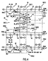
- this MPSR 16 includes portions of the serial scan chains 26 (which portions are indicated on Figure 3 with the numeral 126 also having a parenthetical suffix added which corresponds to those suffixes of Figures 1 and 2.
- the MPSR 16 also includes the especially configured SRAM facility 28, and a dual ported scan register control 30.
- a parallel connection 32 (one of plural being illustrated in detail - see the parenthetical suffixes) provides for parallel data exchange between selected scan chains (i.e., 26(1) thru 26(M)), and the SRAM facility 28, which also may be referred to as a register.
- each scan register in the scan chains 26(1), 26(2), through 26(n) includes two registers, a master register 34, and a slave register 36. These two registers 34 and 36 work together to move data through a serial string of scan register portions 38 (the first being indicated, and subsequent register portions being indicated by the rightwardly directed arrows on Figure 4 and the reference character 38(+).
- This data movement through the register portions is effected by pulsing non-overlapping respective clocks, indicated as master clock 40, and slave clock 42 (connection points for these clock signals being indicated). It is noted on Figure 4 that additional respective pairs of such non-overlapping clock connections are indicated for the additional scan chains through the number "N" of the array
- Each scan register portion 34 is associated with a plurality of SRAM memory cells 44, the number of memory cells 44 in a SRAM register portion depending on the number of the data words to be moved between the scan register portions 34.
- the depth of the plurality of memory cells 44 illustrated in Figure 4 is exemplary only, and is not a limitation on the invention. Accordingly, these plural memory cells are indicated with characters 44(1) through 44(k), where "k" in this case indicates the number of memory cells in the SRAM register associated with each portion of the scan chain register 34.
- Each memory cell 44 includes a pair of cross-coupled inverters 46, 48 (only one of the cells being so referenced in Figure 4 because of space limitations on the drawing Figure 4) respectively connected to a pair of bit lines 50, 52 through a of select transistors 54, 56 (again, only a pair of each out of a large plurality being so referenced on Figure 4 because of space limitations on the drawing Figure 4).
- Data is written into a selected SRAM memory cell from a selected scan chain containing the master register 34 through select transistors 54 and 56 and select transistors 60.
- data is written into a selected scan chain slave register 36 from a selected SRAM memory cell 44 through select transistors 54 and 56 and select transistors 58.
- the write transistors 60 with gate controls labeled "write 1,” “write 2,” through “write M,” on Figure 4 pass data from the selected scan chain master register 34 to a selected SRAM memory cell 44.
- the basic SRAM memory circuit of Figures 4 includes, SRAM memory cells, and decoders, as will be seen.
- the decoder circuits are configured to connect selected SRAM memory cells to selected scan chains. Data is read from one portion of the selected scan chains (i.e., the master registers 34) and is written in a different portion of the selected scan chains (i.e., into the slave registers 36). Reading data from an SRAM employs a clocked slave register to switch the slave register inverters (i.e., inverters are not referenced individually in Figure 4, but are shown as part of the slave scan register 36, and they are clocked inverters with the control signals R1_SA, R2_SA, through RM_SA) into a high impedance state.
- the SRAM bit lines 50 and 52 are equalized (i.e., by temporarily switching transistor 62 to a conductive state and then back to a non-conductive state) to prevent stored charge on the slave register from disrupting the data stored in the SRAM memory cell 44 being read, then the word line on the selected row of the SRAM cells is asserted (i.e., by turning on transistors 54 and 56).
- the SRAM data is thus placed on the bit lines that are connected to the selected slave register 36 through transistors 58.
- This data signal at this point may be only a small differential voltage depending on values of the circuit elements.
- the clock on the slave registers then turns on the slave register inverters (i.e., switches them to a low impedance state).
- the differential voltage on the slave register is amplified to a full logic value signal, completing the read operation.
- the number of SRAM memory units 44 linking these scan chains 26 is indeterminate and is variable at choice.
- the number of SRAM memory units 44 utilized will depend in part on the degree of freedom it is wished to achieve and allow for the interconnected scan chains to shift data during a data sharing (i.e., data exchanging operation) among the plurality of scan chains 26. Further, the depth of the SRAM cells 44 may exceed the length of the data words to be transferred in order to allow the SRAM cells to provide a greater volume of data storage.
- the stored data in the SRAM cells 44 is actually data that is in the process of being shared among the scan chains 26.
- this greater storage capacity i.e., when the number of SRAM cells 44 exceeds the length of the data words
- this greater storage capacity could be used to permit multiple passes of one scan chain (i.e., internal memory I/O) to load data from multiple data accesses into temporary SRAM storage for transfer to memory I/O ports (recalling I/O port 24 of Figure 1) at a time shifted so that a host device is then ready to receive the data from the memory unit 10.
- An alternative use of such an extra depth (i.e., greater depth than the length of the data words) of temporary storage in the SRAM cells 44 effected in the SRAM units interconnecting scan chains 26 could be to hold pre-loaded data that may be frequently read into the memory unit 10 (BIST data, for example).
- the number of extra SRAM memory units 44 that are added to the scan chain registers 26 is limited only by the performance of the memory unit 10 which is desired, and by the data transfer performance of the scan registers (i.e., in the case of MRAM memory being employed).
- the maximum number of SRAM memory units 44 is currently estimated to be about one thousand (1000), although this should not be considered as a limitation on the invention because the performance of various types of memory devices, including MRAM memory, is improving, and is expected to further improve in the future.
- FIG. 5 this flow chart shows the steps in exchanging a pair of data bits between two exemplary scan chain registers. Rather than reiterate here each step and sub-step of the process illustrated in Figure 5, the reader is directed to this Figure, and only highlights are discussed in greater detail immediately below.
- Step one (1) of Figure 5 explains that the scan chains (here identified as Scan Chain A, and as Scan Chain B) each independently shift the data bits to be exchanged to respective ports (i.e., interfaces of the respective scan chain register with a SRAM memory unit).
- step two (2) of Figure 5 the "A" scan chain shifts the respective data in parallel into a selected row of a connecting SRAM memory unit.
- Step (2) of Figure 5 it is seen that this shifting of the date in parallel for each bit involves the use of three sub-steps, labeled (a), (b), and (c). These sub-steps are articulated both in flow charting short hand, and in abbreviated plain language on Figure 5.
- Sub-step (a) involves the connection of a selected SRAM cell to bit line (BL on Figure 4) and bit line b (BLb on Figure 4).
- Sub-step (b) is that actual writing of the data hit value to these bit lines, and hence into the SRAM register.
- Sub-step (c) de-selects the bit lines BL and BLb (recalling the explanation of Figure 4 again).
- step three (3) of Figure 5 the "B" scan chain shifts its respective data in parallel into another row of the connecting SRAM memory unit.
- steps four (4) and five (5) of Figure 5 explain that the connecting SRAM memory units later write the respective data bits into the recipient scan chains (i.e., the data bit from scan chain "A” is written into scan chain "B,” and the data bit from scan chain “B” is written into scan chain "A”).
- the term "HIZ” means "high impedance” (recall the explanation above of how data is written to a slave register 36 of selected SRAM memory cell 44 through select transistors 54 and 56 and select transistors 58, while the inverters in the slave register are clocked to a high impedance state with signals R1_SA, R2_SA, through RM_SA).
Claims (10)
- Eine Vorrichtung zum Austauschen von Daten zwischen Abtastketten, die folgende Merkmale aufweist:eine Mehrzahl von Abtastketten (26), wobei jede derselben eine Mehrzahl von Registern umfasst, die in der Lage sind, Datenbits zu speichern, wobei die Mehrzahl von Registern Master-Register (34) und Slave-Register (36) umfasst; undein Array aus mehreren Statischer-Direktzugriffsspeicher-Zellen (SRAM-Zellen) (44), die die Mehrzahl von Abtastketten (26) verbinden, wobei das Array aus mehreren SRAM-Speicherzellen (44) wirksam ist, um Datenbits von Ausgewählten aus den Master-Registern (34) zu empfangen und die Datenbits in Ausgewählte aus den Slave-Registern (36) zu schreiben.
- Eine Vorrichtung gemäß Anspruch 1, die eine parallele Datenverbindung zwischen der Mehrzahl von Abtastketten (26) und dem Array aus SRAM-Speicherzellen (44) umfasst.
- Eine Vorrichtung gemäß Anspruch 1 oder 2, bei der jede SRAM-Speicherzelle des Arrays aus SRAM-Speicherzellen (44) ein Paar aus Invertern (46, 48) umfasst, die miteinander kreuzgekoppelt sind.
- Eine Vorrichtung gemäß Anspruch 3, bei der jede SRAM-Speicherzelle des Arrays aus SRAM-Speicherzellen (44) ein Paar aus Auswahl-Schaltern (54, 56) umfasst, wobei einer des Paars aus Schaltern (54, 56) mit einer Seite des Paars aus kreuzgekoppelten Invertern (46, 48) verbunden ist und der andere des Paars aus Schaltern (54, 56) mit der gegenüberliegenden Seite des Paars aus kreuzgekoppelten Invertern (46, 48) verbunden ist.
- Eine Vorrichtung gemäß Anspruch 4, die einen Ausgleichsschalter (62) umfasst, der über das Paar aus kreuzgekoppelten Invertern (46, 48) und über das Paar aus Auswahl-Schaltern (54, 56) einer SRAM-Speicherzelle verbindet.
- Eine Vorrichtung gemäß Anspruch 5, bei der der Ausgleichsschalter (62) einen Transistor umfasst.
- Eine Vorrichtung gemäß einem der Ansprüche 3 bis 6, die ein Paar aus Schreibschaltern (60) umfasst, die eine gemeinsame Schalter-Verschluß-Steuerverbindung umfassen, und bei der jeder des Paars aus Schreibschaltern (60) eine entsprechende eine Seite des Paars aus kreuzgekoppelten Invertern (46, 48) mit einer entsprechenden Seite eines Registers von einer des Paars der Abtastketten (26) verbindet.
- Eine Vorrichtung gemäß Anspruch 7, bei der das Paar aus Schreibschaltern (60) eine Verbindung mit einem Master-Register (34) der einen Abtastkette (26) herstellt.
- Eine Vorrichtung gemäß einem der Ansprüche 3 bis 8, die ein Paar aus Leseschaltern (58) umfasst, die eine gemeinsame Schalter-Verschluß-Steuerverbindung aufweisen, und bei der jeder der Leseschalter (58) eine entsprechende eine Seite des Paars aus kreuzgekoppelten Invertern (46, 48) mit einer entsprechenden Seite eines Registers von einer des Paars aus Abtastketten (26) verbindet.
- Eine Vorrichtung gemäß Anspruch 9, bei der das Paar aus Leseschaltern (58) mit einem Slave-Register der einen Abtastkette (26) verbunden ist.
Applications Claiming Priority (2)
| Application Number | Priority Date | Filing Date | Title |
|---|---|---|---|
| US10/107,939 US6848067B2 (en) | 2002-03-27 | 2002-03-27 | Multi-port scan chain register apparatus and method |
| US107939 | 2002-03-27 |
Publications (2)
| Publication Number | Publication Date |
|---|---|
| EP1349171A1 EP1349171A1 (de) | 2003-10-01 |
| EP1349171B1 true EP1349171B1 (de) | 2005-12-21 |
Family
ID=27804376
Family Applications (1)
| Application Number | Title | Priority Date | Filing Date |
|---|---|---|---|
| EP03251315A Expired - Lifetime EP1349171B1 (de) | 2002-03-27 | 2003-03-05 | Data-Austauschvorrichtung zwischen Abtastketten |
Country Status (7)
| Country | Link |
|---|---|
| US (1) | US6848067B2 (de) |
| EP (1) | EP1349171B1 (de) |
| JP (1) | JP2003308224A (de) |
| KR (1) | KR100944179B1 (de) |
| CN (1) | CN100403446C (de) |
| DE (1) | DE60302821T2 (de) |
| TW (1) | TW200304546A (de) |
Families Citing this family (23)
| Publication number | Priority date | Publication date | Assignee | Title |
|---|---|---|---|---|
| US9984377B2 (en) * | 2003-10-06 | 2018-05-29 | Yellowpages.Com Llc | System and method for providing advertisement |
| US7027323B2 (en) * | 2004-04-02 | 2006-04-11 | Hewlett-Packard Development Company, L.P. | Storage device having parallel connected memory cells that include magnetoresistive elements |
| US7362549B2 (en) * | 2004-05-19 | 2008-04-22 | Seagate Technology Llc | Storage device having first and second magnetic elements that interact magnetically to indicate a storage state |
| KR100632367B1 (ko) | 2004-11-22 | 2006-10-09 | 삼성전자주식회사 | 불휘발성 반도체 메모리 장치의 프로그램 비트 스캔표시회로 |
| US8429319B2 (en) * | 2005-09-28 | 2013-04-23 | Hynix Semiconductor Inc. | Multi-port memory device with serial input/output interface |
| CN1996035B (zh) * | 2005-12-31 | 2012-01-25 | 旺玖科技股份有限公司 | 用于多芯片组件的具有可规划扫描链的装置 |
| US7600168B2 (en) * | 2005-12-26 | 2009-10-06 | Prolific Technology Inc. | Apparatus with programmable scan chains for multiple chip modules and method for programming the same |
| US7388776B1 (en) * | 2006-12-22 | 2008-06-17 | Hitachi Global Storage Technologies Netherlands, B.V. | Three-dimensional magnetic memory |
| US8434153B2 (en) | 2009-08-24 | 2013-04-30 | Microsoft Corporation | Application display on a locked device |
| CN102043124B (zh) * | 2009-10-12 | 2013-07-17 | 炬力集成电路设计有限公司 | 一种具有扫描链的集成电路 |
| US8315081B2 (en) | 2010-03-22 | 2012-11-20 | Qualcomm Incorporated | Memory cell that includes multiple non-volatile memories |
| JP2011216657A (ja) * | 2010-03-31 | 2011-10-27 | Unisantis Electronics Japan Ltd | 半導体装置 |
| US8694844B2 (en) | 2010-07-29 | 2014-04-08 | Texas Instruments Incorporated | AT speed TAP with dual port router and command circuit |
| US8438433B2 (en) * | 2010-09-21 | 2013-05-07 | Qualcomm Incorporated | Registers with full scan capability |
| CN102109978A (zh) * | 2011-02-28 | 2011-06-29 | 孙瑞琛 | 一种数据的重排方法及重排装置 |
| KR101929983B1 (ko) | 2012-07-18 | 2018-12-17 | 삼성전자주식회사 | 저항성 메모리 셀을 갖는 반도체 메모리 장치 및 그 테스트 방법 |
| US8788897B2 (en) * | 2012-09-28 | 2014-07-22 | Texas Instruments Incorporated | Path-based crosstalk fault test scanning in built-in self-testing |
| US9651618B2 (en) | 2013-01-09 | 2017-05-16 | Nxp Usa, Inc. | Electronic device and method for state retention |
| JP2014137292A (ja) * | 2013-01-17 | 2014-07-28 | Fujitsu Semiconductor Ltd | スキャン回路、半導体装置および半導体装置の試験方法 |
| US20150316971A1 (en) * | 2014-05-02 | 2015-11-05 | Avalanche Technology, Inc. | Method and apparatus to reduce power consumption of mobile and portable devices with non-volatile memories |
| JP6305823B2 (ja) * | 2014-05-12 | 2018-04-04 | 株式会社メガチップス | スキャンテスト回路 |
| CN104943397B (zh) | 2015-06-25 | 2016-08-17 | 珠海艾派克微电子有限公司 | 成像盒芯片、成像盒以及更换成像盒芯片序列号的方法 |
| CN109901048B (zh) * | 2017-12-09 | 2021-04-27 | 英业达科技有限公司 | 以不同扫描链测试差分线路的系统及其方法 |
Family Cites Families (13)
| Publication number | Priority date | Publication date | Assignee | Title |
|---|---|---|---|---|
| JPS62287497A (ja) * | 1986-06-06 | 1987-12-14 | Fujitsu Ltd | 半導体記憶装置 |
| FR2624631B1 (fr) | 1987-12-14 | 1990-05-04 | Centre Nat Rech Scient | Systeme multiprocesseur, procede d'echange d'informations mis en oeuvre et composant memoire multiport serie susceptible d'equiper ledit systeme |
| US5442770A (en) * | 1989-01-24 | 1995-08-15 | Nec Electronics, Inc. | Triple port cache memory |
| JPH0682326B2 (ja) | 1989-09-29 | 1994-10-19 | 三菱電機株式会社 | スキャンレジスタおよびそれを用いたテスト回路 |
| US5452259A (en) * | 1993-11-15 | 1995-09-19 | Micron Technology Inc. | Multiport memory with pipelined serial input |
| GB9405804D0 (en) * | 1994-03-24 | 1994-05-11 | Discovision Ass | Scannable latch and method of using the same |
| JP2734394B2 (ja) | 1995-01-27 | 1998-03-30 | 日本電気株式会社 | 半導体集積回路装置 |
| US5867507A (en) | 1995-12-12 | 1999-02-02 | International Business Machines Corporation | Testable programmable gate array and associated LSSD/deterministic test methodology |
| US5636228A (en) | 1996-01-16 | 1997-06-03 | Motorola, Inc. | Scan register with decoupled scan routing |
| US6816490B1 (en) * | 1997-09-17 | 2004-11-09 | Sony Corporation | Statistical learning technique in a multi-port bridge for a local area network |
| US5953285A (en) | 1997-09-17 | 1999-09-14 | Cypress Semiconductor Corp. | Scan path circuitry including an output register having a flow through mode |
| US6728799B1 (en) * | 2000-01-13 | 2004-04-27 | Hewlett-Packard Development Company, L.P. | Hybrid data I/O for memory applications |
| JP2001243763A (ja) * | 2000-02-24 | 2001-09-07 | Nec Microsystems Ltd | 半導体記憶装置およびそのバンク間データ転送方法 |
-
2002
- 2002-03-27 US US10/107,939 patent/US6848067B2/en not_active Expired - Lifetime
-
2003
- 2003-01-15 TW TW092100813A patent/TW200304546A/zh unknown
- 2003-03-05 DE DE60302821T patent/DE60302821T2/de not_active Expired - Lifetime
- 2003-03-05 EP EP03251315A patent/EP1349171B1/de not_active Expired - Lifetime
- 2003-03-26 KR KR1020030018735A patent/KR100944179B1/ko active IP Right Grant
- 2003-03-27 CN CNB031083013A patent/CN100403446C/zh not_active Expired - Lifetime
- 2003-03-27 JP JP2003087447A patent/JP2003308224A/ja active Pending
Also Published As
| Publication number | Publication date |
|---|---|
| US6848067B2 (en) | 2005-01-25 |
| TW200304546A (en) | 2003-10-01 |
| KR100944179B1 (ko) | 2010-02-25 |
| JP2003308224A (ja) | 2003-10-31 |
| DE60302821T2 (de) | 2006-08-10 |
| CN1447335A (zh) | 2003-10-08 |
| EP1349171A1 (de) | 2003-10-01 |
| KR20030078007A (ko) | 2003-10-04 |
| US20030188240A1 (en) | 2003-10-02 |
| CN100403446C (zh) | 2008-07-16 |
| DE60302821D1 (de) | 2006-01-26 |
Similar Documents
| Publication | Publication Date | Title |
|---|---|---|
| EP1349171B1 (de) | Data-Austauschvorrichtung zwischen Abtastketten | |
| USRE40894E1 (en) | Sample and load scheme for observability internal nodes in a PLD | |
| US6876228B2 (en) | Field programmable gate array | |
| US6646903B2 (en) | Ferroelectric memory input/output apparatus | |
| JP2891504B2 (ja) | マルチポートメモリ | |
| EP0179605B1 (de) | Halbleiterspeicheranordnung mit einer seriellen Dateneingangs- und Ausgangsschaltung | |
| KR950003605B1 (ko) | 반도체 기억장치 | |
| EP1251520B1 (de) | Direktzugriffsspeicher | |
| US9466352B2 (en) | Dynamic/static random access memory (D/SRAM) | |
| EP0121726A2 (de) | Mehr-Tore-Speicherzelle und System | |
| JP3319637B2 (ja) | 半導体記憶装置及びその制御方法 | |
| US8862836B2 (en) | Multi-port register file with an input pipelined architecture with asynchronous reads and localized feedback | |
| US6091627A (en) | Message box memory cell for two-side asynchronous access | |
| EP1612804B1 (de) | Magnetischer RAM Speicher (MRAM) mit mehr als einem Bit pro Speicherzelle | |
| US20040257860A1 (en) | Bi-directional buffering for memory data lines | |
| US9589623B2 (en) | Word shift static random access memory (WS-SRAM) | |
| JP3035995B2 (ja) | マルチポートメモリ | |
| EP0512536B1 (de) | Programmierbare logische Einheit | |
| US7242633B1 (en) | Memory device and method of transferring data in memory device | |
| US7246300B1 (en) | Sequential flow-control and FIFO memory devices having error detection and correction capability with diagnostic bit generation | |
| JPS62180582A (ja) | 多ポ−トメモリシステム | |
| JPS6364692A (ja) | 半導体メモリ装置 | |
| JPS61194697A (ja) | 半導体装置 |
Legal Events
| Date | Code | Title | Description |
|---|---|---|---|
| PUAI | Public reference made under article 153(3) epc to a published international application that has entered the european phase |
Free format text: ORIGINAL CODE: 0009012 |
|
| AK | Designated contracting states |
Kind code of ref document: A1 Designated state(s): AT BE BG CH CY CZ DE DK EE ES FI FR GB GR HU IE IT LI LU MC NL PT RO SE SI SK TR |
|
| AX | Request for extension of the european patent |
Extension state: AL LT LV MK |
|
| 17P | Request for examination filed |
Effective date: 20040325 |
|
| AKX | Designation fees paid |
Designated state(s): DE GB |
|
| GRAP | Despatch of communication of intention to grant a patent |
Free format text: ORIGINAL CODE: EPIDOSNIGR1 |
|
| GRAS | Grant fee paid |
Free format text: ORIGINAL CODE: EPIDOSNIGR3 |
|
| GRAA | (expected) grant |
Free format text: ORIGINAL CODE: 0009210 |
|
| AK | Designated contracting states |
Kind code of ref document: B1 Designated state(s): DE GB |
|
| REG | Reference to a national code |
Ref country code: GB Ref legal event code: FG4D |
|
| REF | Corresponds to: |
Ref document number: 60302821 Country of ref document: DE Date of ref document: 20060126 Kind code of ref document: P |
|
| PLBE | No opposition filed within time limit |
Free format text: ORIGINAL CODE: 0009261 |
|
| STAA | Information on the status of an ep patent application or granted ep patent |
Free format text: STATUS: NO OPPOSITION FILED WITHIN TIME LIMIT |
|
| 26N | No opposition filed |
Effective date: 20060922 |
|
| REG | Reference to a national code |
Ref country code: GB Ref legal event code: 732E |
|
| PGFP | Annual fee paid to national office [announced via postgrant information from national office to epo] |
Ref country code: GB Payment date: 20220127 Year of fee payment: 20 Ref country code: DE Payment date: 20220126 Year of fee payment: 20 |
|
| REG | Reference to a national code |
Ref country code: DE Ref legal event code: R071 Ref document number: 60302821 Country of ref document: DE |
|
| REG | Reference to a national code |
Ref country code: GB Ref legal event code: PE20 Expiry date: 20230304 |
|
| PG25 | Lapsed in a contracting state [announced via postgrant information from national office to epo] |
Ref country code: GB Free format text: LAPSE BECAUSE OF EXPIRATION OF PROTECTION Effective date: 20230304 |