EP1348778B1 - Method for obtaining high quality InGaAsN semiconductor - Google Patents
Method for obtaining high quality InGaAsN semiconductor Download PDFInfo
- Publication number
- EP1348778B1 EP1348778B1 EP02023298A EP02023298A EP1348778B1 EP 1348778 B1 EP1348778 B1 EP 1348778B1 EP 02023298 A EP02023298 A EP 02023298A EP 02023298 A EP02023298 A EP 02023298A EP 1348778 B1 EP1348778 B1 EP 1348778B1
- Authority
- EP
- European Patent Office
- Prior art keywords
- layer
- growth
- ingaasn
- range
- gaas
- Prior art date
- Legal status (The legal status is an assumption and is not a legal conclusion. Google has not performed a legal analysis and makes no representation as to the accuracy of the status listed.)
- Expired - Lifetime
Links
Images


Classifications
-
- C—CHEMISTRY; METALLURGY
- C30—CRYSTAL GROWTH
- C30B—SINGLE-CRYSTAL GROWTH; UNIDIRECTIONAL SOLIDIFICATION OF EUTECTIC MATERIAL OR UNIDIRECTIONAL DEMIXING OF EUTECTOID MATERIAL; REFINING BY ZONE-MELTING OF MATERIAL; PRODUCTION OF A HOMOGENEOUS POLYCRYSTALLINE MATERIAL WITH DEFINED STRUCTURE; SINGLE CRYSTALS OR HOMOGENEOUS POLYCRYSTALLINE MATERIAL WITH DEFINED STRUCTURE; AFTER-TREATMENT OF SINGLE CRYSTALS OR A HOMOGENEOUS POLYCRYSTALLINE MATERIAL WITH DEFINED STRUCTURE; APPARATUS THEREFOR
- C30B25/00—Single-crystal growth by chemical reaction of reactive gases, e.g. chemical vapour-deposition growth
- C30B25/02—Epitaxial-layer growth
-
- C—CHEMISTRY; METALLURGY
- C23—COATING METALLIC MATERIAL; COATING MATERIAL WITH METALLIC MATERIAL; CHEMICAL SURFACE TREATMENT; DIFFUSION TREATMENT OF METALLIC MATERIAL; COATING BY VACUUM EVAPORATION, BY SPUTTERING, BY ION IMPLANTATION OR BY CHEMICAL VAPOUR DEPOSITION, IN GENERAL; INHIBITING CORROSION OF METALLIC MATERIAL OR INCRUSTATION IN GENERAL
- C23C—COATING METALLIC MATERIAL; COATING MATERIAL WITH METALLIC MATERIAL; SURFACE TREATMENT OF METALLIC MATERIAL BY DIFFUSION INTO THE SURFACE, BY CHEMICAL CONVERSION OR SUBSTITUTION; COATING BY VACUUM EVAPORATION, BY SPUTTERING, BY ION IMPLANTATION OR BY CHEMICAL VAPOUR DEPOSITION, IN GENERAL
- C23C16/00—Chemical coating by decomposition of gaseous compounds, without leaving reaction products of surface material in the coating, i.e. chemical vapour deposition [CVD] processes
- C23C16/22—Chemical coating by decomposition of gaseous compounds, without leaving reaction products of surface material in the coating, i.e. chemical vapour deposition [CVD] processes characterised by the deposition of inorganic material, other than metallic material
- C23C16/30—Deposition of compounds, mixtures or solid solutions, e.g. borides, carbides, nitrides
- C23C16/301—AIII BV compounds, where A is Al, Ga, In or Tl and B is N, P, As, Sb or Bi
-
- C—CHEMISTRY; METALLURGY
- C23—COATING METALLIC MATERIAL; COATING MATERIAL WITH METALLIC MATERIAL; CHEMICAL SURFACE TREATMENT; DIFFUSION TREATMENT OF METALLIC MATERIAL; COATING BY VACUUM EVAPORATION, BY SPUTTERING, BY ION IMPLANTATION OR BY CHEMICAL VAPOUR DEPOSITION, IN GENERAL; INHIBITING CORROSION OF METALLIC MATERIAL OR INCRUSTATION IN GENERAL
- C23C—COATING METALLIC MATERIAL; COATING MATERIAL WITH METALLIC MATERIAL; SURFACE TREATMENT OF METALLIC MATERIAL BY DIFFUSION INTO THE SURFACE, BY CHEMICAL CONVERSION OR SUBSTITUTION; COATING BY VACUUM EVAPORATION, BY SPUTTERING, BY ION IMPLANTATION OR BY CHEMICAL VAPOUR DEPOSITION, IN GENERAL
- C23C16/00—Chemical coating by decomposition of gaseous compounds, without leaving reaction products of surface material in the coating, i.e. chemical vapour deposition [CVD] processes
- C23C16/44—Chemical coating by decomposition of gaseous compounds, without leaving reaction products of surface material in the coating, i.e. chemical vapour deposition [CVD] processes characterised by the method of coating
- C23C16/4401—Means for minimising impurities, e.g. dust, moisture or residual gas, in the reaction chamber
-
- C—CHEMISTRY; METALLURGY
- C23—COATING METALLIC MATERIAL; COATING MATERIAL WITH METALLIC MATERIAL; CHEMICAL SURFACE TREATMENT; DIFFUSION TREATMENT OF METALLIC MATERIAL; COATING BY VACUUM EVAPORATION, BY SPUTTERING, BY ION IMPLANTATION OR BY CHEMICAL VAPOUR DEPOSITION, IN GENERAL; INHIBITING CORROSION OF METALLIC MATERIAL OR INCRUSTATION IN GENERAL
- C23C—COATING METALLIC MATERIAL; COATING MATERIAL WITH METALLIC MATERIAL; SURFACE TREATMENT OF METALLIC MATERIAL BY DIFFUSION INTO THE SURFACE, BY CHEMICAL CONVERSION OR SUBSTITUTION; COATING BY VACUUM EVAPORATION, BY SPUTTERING, BY ION IMPLANTATION OR BY CHEMICAL VAPOUR DEPOSITION, IN GENERAL
- C23C16/00—Chemical coating by decomposition of gaseous compounds, without leaving reaction products of surface material in the coating, i.e. chemical vapour deposition [CVD] processes
- C23C16/44—Chemical coating by decomposition of gaseous compounds, without leaving reaction products of surface material in the coating, i.e. chemical vapour deposition [CVD] processes characterised by the method of coating
- C23C16/4401—Means for minimising impurities, e.g. dust, moisture or residual gas, in the reaction chamber
- C23C16/4405—Cleaning of reactor or parts inside the reactor by using reactive gases
-
- C—CHEMISTRY; METALLURGY
- C30—CRYSTAL GROWTH
- C30B—SINGLE-CRYSTAL GROWTH; UNIDIRECTIONAL SOLIDIFICATION OF EUTECTIC MATERIAL OR UNIDIRECTIONAL DEMIXING OF EUTECTOID MATERIAL; REFINING BY ZONE-MELTING OF MATERIAL; PRODUCTION OF A HOMOGENEOUS POLYCRYSTALLINE MATERIAL WITH DEFINED STRUCTURE; SINGLE CRYSTALS OR HOMOGENEOUS POLYCRYSTALLINE MATERIAL WITH DEFINED STRUCTURE; AFTER-TREATMENT OF SINGLE CRYSTALS OR A HOMOGENEOUS POLYCRYSTALLINE MATERIAL WITH DEFINED STRUCTURE; APPARATUS THEREFOR
- C30B29/00—Single crystals or homogeneous polycrystalline material with defined structure characterised by the material or by their shape
- C30B29/10—Inorganic compounds or compositions
- C30B29/40—AIIIBV compounds wherein A is B, Al, Ga, In or Tl and B is N, P, As, Sb or Bi
- C30B29/403—AIII-nitrides
-
- H—ELECTRICITY
- H10—SEMICONDUCTOR DEVICES; ELECTRIC SOLID-STATE DEVICES NOT OTHERWISE PROVIDED FOR
- H10P—GENERIC PROCESSES OR APPARATUS FOR THE MANUFACTURE OR TREATMENT OF DEVICES COVERED BY CLASS H10
- H10P14/00—Formation of materials, e.g. in the shape of layers or pillars
- H10P14/20—Formation of materials, e.g. in the shape of layers or pillars of semiconductor materials
- H10P14/24—Formation of materials, e.g. in the shape of layers or pillars of semiconductor materials using chemical vapour deposition [CVD]
-
- H—ELECTRICITY
- H10—SEMICONDUCTOR DEVICES; ELECTRIC SOLID-STATE DEVICES NOT OTHERWISE PROVIDED FOR
- H10P—GENERIC PROCESSES OR APPARATUS FOR THE MANUFACTURE OR TREATMENT OF DEVICES COVERED BY CLASS H10
- H10P14/00—Formation of materials, e.g. in the shape of layers or pillars
- H10P14/20—Formation of materials, e.g. in the shape of layers or pillars of semiconductor materials
- H10P14/29—Formation of materials, e.g. in the shape of layers or pillars of semiconductor materials characterised by the substrates
- H10P14/2901—Materials
- H10P14/2907—Materials being Group IIIA-VA materials
- H10P14/2911—Arsenides
-
- H—ELECTRICITY
- H10—SEMICONDUCTOR DEVICES; ELECTRIC SOLID-STATE DEVICES NOT OTHERWISE PROVIDED FOR
- H10P—GENERIC PROCESSES OR APPARATUS FOR THE MANUFACTURE OR TREATMENT OF DEVICES COVERED BY CLASS H10
- H10P14/00—Formation of materials, e.g. in the shape of layers or pillars
- H10P14/20—Formation of materials, e.g. in the shape of layers or pillars of semiconductor materials
- H10P14/32—Formation of materials, e.g. in the shape of layers or pillars of semiconductor materials characterised by intermediate layers between substrates and deposited layers
- H10P14/3202—Materials thereof
- H10P14/3214—Materials thereof being Group IIIA-VA semiconductors
- H10P14/3221—Arsenides
-
- H—ELECTRICITY
- H10—SEMICONDUCTOR DEVICES; ELECTRIC SOLID-STATE DEVICES NOT OTHERWISE PROVIDED FOR
- H10P—GENERIC PROCESSES OR APPARATUS FOR THE MANUFACTURE OR TREATMENT OF DEVICES COVERED BY CLASS H10
- H10P14/00—Formation of materials, e.g. in the shape of layers or pillars
- H10P14/20—Formation of materials, e.g. in the shape of layers or pillars of semiconductor materials
- H10P14/32—Formation of materials, e.g. in the shape of layers or pillars of semiconductor materials characterised by intermediate layers between substrates and deposited layers
- H10P14/3242—Structure
- H10P14/3244—Layer structure
- H10P14/3251—Layer structure consisting of three or more layers
- H10P14/3252—Alternating layers, e.g. superlattice
-
- H—ELECTRICITY
- H10—SEMICONDUCTOR DEVICES; ELECTRIC SOLID-STATE DEVICES NOT OTHERWISE PROVIDED FOR
- H10P—GENERIC PROCESSES OR APPARATUS FOR THE MANUFACTURE OR TREATMENT OF DEVICES COVERED BY CLASS H10
- H10P14/00—Formation of materials, e.g. in the shape of layers or pillars
- H10P14/20—Formation of materials, e.g. in the shape of layers or pillars of semiconductor materials
- H10P14/34—Deposited materials, e.g. layers
- H10P14/3402—Deposited materials, e.g. layers characterised by the chemical composition
- H10P14/3414—Deposited materials, e.g. layers characterised by the chemical composition being group IIIA-VIA materials
- H10P14/3416—Nitrides
-
- H—ELECTRICITY
- H10—SEMICONDUCTOR DEVICES; ELECTRIC SOLID-STATE DEVICES NOT OTHERWISE PROVIDED FOR
- H10P—GENERIC PROCESSES OR APPARATUS FOR THE MANUFACTURE OR TREATMENT OF DEVICES COVERED BY CLASS H10
- H10P14/00—Formation of materials, e.g. in the shape of layers or pillars
- H10P14/20—Formation of materials, e.g. in the shape of layers or pillars of semiconductor materials
- H10P14/34—Deposited materials, e.g. layers
- H10P14/3402—Deposited materials, e.g. layers characterised by the chemical composition
- H10P14/3414—Deposited materials, e.g. layers characterised by the chemical composition being group IIIA-VIA materials
- H10P14/3421—Arsenides
-
- H—ELECTRICITY
- H10—SEMICONDUCTOR DEVICES; ELECTRIC SOLID-STATE DEVICES NOT OTHERWISE PROVIDED FOR
- H10P—GENERIC PROCESSES OR APPARATUS FOR THE MANUFACTURE OR TREATMENT OF DEVICES COVERED BY CLASS H10
- H10P14/00—Formation of materials, e.g. in the shape of layers or pillars
- H10P14/20—Formation of materials, e.g. in the shape of layers or pillars of semiconductor materials
- H10P14/34—Deposited materials, e.g. layers
- H10P14/3438—Doping during depositing
- H10P14/3441—Conductivity type
- H10P14/3444—P-type
Definitions
- the invention relates to a method for making high quality InGaAsN semiconductor devices using metal organic chemical vapor deposition.
- InGaAsN is an attractive material for a variety of semiconductor applications. InGaAsN is useful in the area of long wavelength edge-emitting lasers and vertical cavity surface emitting lasers (VCSEL) as disclosed in WO 01/52373 in the optical communications area because the material is readily grown on GaAs wafers which provides higher conduction band offset and allows me use of GaAs/AlAs high reflective distributed Bragg reflectors (DBRs).
- VCSEL vertical cavity surface emitting lasers
- CW room temperature continuous wave
- MBE molecular beam epitaxy
- InGaAsN active regions grown over AIGaAs layers show more O and C incorporation than InGaAsN active regions grown without underlying AIGaAs layers.
- either layers are grown in the semiconductor structure whose growth serves to getter Al atoms/Al containing molecules or chemicals may be introduced into the MOCVD chamber via flow gases that serve to getter Al atoms/Al containing molecules.
- the methods reduce the Al content that is incorporated into the N containing layers and result in improvements in the quality of the InGaAsN layer including smoother surface structure, improved optical qualities and lower levels of recombination centers due to, for example, O and C incorporation that typically accompanies the Al incorporation.
- methods are disclosed to control incorporation of Al from the growth of Al containing layers such as AlGaAs layers into active InGaAsN layers that are grown continuously on GaAs/AlGaAs. These methods typically involve either the growth of layers in the semiconductor device that serves to getter Al atoms/Al containing molecules or the introduction of chemicals into the MOCVD chamber with flow gases that serve to getter Al atoms/Al containing molecules without accompanying layer growth.
- layers whose growth also functions to getter Al atoms or molecules containing Al can be grown at any time before the growth of the InGaAsN layer or between growth of the InGaAsN active layer and the previously grown AIGaAs layer to reduce Al contamination of the InGaAsN active layer.
- layers whose growth involves atoms/molecules which react more effectively with Al or Al containing molecules than As atoms or molecules containing As are suitable.
- growth of layers that contain N and/or P atoms is typically effective in reducing the Al contamination when the total amount ofN and/or P atoms introduced into the MOCVD reactor is greater than the amount of Al atoms that are introduced into the MOCVD reactor prior to the growth of the InGaAsN active layer.
- the absolute amounts will be MOCVD reactor specific.
- the flow rate of the Al gettering chemical and time of application is determined by setting the total amount of gettering atoms such as N and/or P introduced by the flow to be greater than the total amount of Al introduced into the reactor chamber.
- chemicals that getter Al atoms /Al containing molecules may be introduced via flow gases into the MOCVD reactor anytime before growth of the InGaAsN layer or anytime before growth of the InGaAsN layer and after growth of the AlGaAs layer to reduce Al contamination of the InGaAsN layer.
- chemicals that can react more effectively with Al atoms/Al containing molecules than As atoms or molecules containing As are introduced via flow gases into the MOCVD reactor anytime before growing the InGaAsN layer or anytime before growth of the InGaAsN layer and after the growth of the AlGaAs layer.
- introduction of chemicals that contain N and/or P atoms via flow gases into the MOCVD is typically effective when the total amount ofN and/or P atoms in the chemicals is greater than the total number of Al atoms that are introduced before the InGasAsN layer is grown.
- any semiconductor devices using InGaAsN layers and Al containing layers such as AlGaAs, AlGaInP and AlGaInAsP may be made using a single reactor MOCVD process while obtaining high quality InGaAsN layers having low levels of Al contamination.
- solar cell and photodetector device structure using high quality InGaAsN absorbing layers results in higher quantum efficiencies while bipolar transistors using InGaAsN collector and base layers suffer less from the presence of recombination centers which lead to low current gain.
- FIG. 1a shows MOCVD reactor 120 in side view with exhaust line 180.
- MOCVD reactor 120 is a cold wall, quartz reactor.
- Group-III source injection occurs at inlet 125 and Group- V source injection occurs at inlet 130.
- Group III and Group V gases begin mixing after passing from outlets 187 and 188.
- Outlets 187 and 188 are both approximately 13 cm x 2 cm rectangles.
- Vertical height 143 of MOCVD reactor 120 is approximately 4.5 cm while dimension 144 is approximately 3 cm.
- Dimension 148 is approximately 7 cm and is the distance from where the Group III and Group V gases begin to mix to where the vertical constriction of MOCVD reactor 120 starts.
- Dimension 147 is approximately 7 cm and SiC-coated graphite susceptor 170 has diameter 146 of approximately 11 cm with thickness 145 of approximately 1.5 cm. Substrate 175 is positioned on susceptor 170 as shown in FIGS. 1 a and 1b. With reference to FIG. 1 b, lateral dimension 185 of MOCVD reactor 120 is approximately 13 cm while dimension 149 is approximately 1.5 cm.
- FIG. 2 shows an arrangement of the chemicals and lines feeding into MOCVD reactor 120.
- MOCVD reactor 120 is typically a cold wall, quartz reactor.
- Valves 250, 251, 252 and 253 control and direct flow from tanks 231, 232, 233, and 234, respectively.
- Valves 254, 255, 256, 257, 258, 259 and 260 control and direct flow from bubblers 235, 236, 237, 23 8, 239, 240 and 24 1, respectively.
- Inlet 210 serves to introduce H 2 carrier gas into MOCVD reactor 120 via line 212 to inlet 130 of MOCVD reactor 120.
- Line 212 serves as well for typically introducing Tertiarybutylarsine (TBAs) from bubbler 235 and Dimethylhydrazine (DMHy) from bubbler 236 into MOCVD reactor 120 via inlet 130.
- Valves 254 and 255 direct flow from bubblers 235 and 236, respectively, into either line 212 or vent line 220.
- Vent lines 220 connect to exhaust line 180.
- Line 221 serves to introduce H 2 into bubblers 235 and 236 while line 222 serves to introduce H 2 into bubblers 237, 238, 239, 240 and 241.
- Line 211 serves to introduce NH 3 from tank 231, AsH 3 from tank 232, PH 3 from tank 233 and Si 2 H 6 from tank 234 into MOVCD reactor 120 via inlet 130.
- Valves 250, 251, 252 and 253 direct flow from tanks 231, 232, 233 and 234, respectively, into either line 211 or vent line 220.
- Line 213 serves to typically introduce Trinnethylgalium (TMGa) from bubbler 237, Triethylgallium (TEGa) from bubbler 238, Trimethyaluminum (TMAI) from bubbler 239, Trimethylindium (TMIn) from bubbler 240 and CBr 4 from bubbler 241 into MOCVD reactor 120 via inlet 125.
- Valves 256, 257, 258, 259 and 260 direct flow from bubblers 237, 238, 239, 240 and 241, respectively, into either line 213 or vent line 220. Note that there is no back flow in any of the lines since a mechanical pump (not shown) maintains the pressure inside reactor 120 at about 100 mbar.
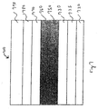
- FIG. 3 shows InGaAsN quantum well photoluminescence (PL) test structure 300 in an embodiment according to the invention.
- GaAs buffer layer 325 typically having a thickness in the range of about 1000 - 5000 ⁇ , is grown on GaAs substrate 320 at a temperature in the range of about 600 - 800 °C using Trimethylgallium (TMGa) and arsine (AsH 3 ) at a pressure in the range of about 50 - 400 mbar H 2 ambient.
- TMGa Trimethylgallium
- AsH 3 arsine
- Al 0.3 Ga 0.7 As layer 330 typically having a thickness of 0.9 ⁇ m, is grown on GaAs buffer layer 325 by introducing Trimethylaluminum (TMAI).
- TMAI Trimethylaluminum
- TMAI is then stopped and GaAs layer 335 is grown to a thickness in the range of about 50 -300 ⁇ .
- the total amount of TMAI supplied is about 4 x 10 -4 mol.
- the growth process is interrupted by shutting off the supply of TMGa.
- a flow of AsH 3 typically at about 300 sccm is continuously introduced into an MOCVD reactor such as MOCVD reactor 120 to prevent degradation of the exposed surface of GaAs layer 335. Surface degradation is typically a problem if the temperature exceeds approximately 400 °C and should be avoided.
- NH 3 (ammonia) is introduced at a typical flow rate of about 500 sccm at a temperature and pressure in the range of about 400 -700 °C and 50 - 1000 mbar, typically at 500 - 600 °C and 100 mbar, respectively.
- NH 3 is attractive for reasons of cost and purity.
- the application time for the NH 3 can be varied, typically from between about 0.5 minutes to about 4 minutes. Longer application times reduce the amount of ambient Al available for incorporation into InGaAsN layer 350 and InGaAsN layer 360.
- An application time of 0.5 minutes at a flow rate of about 500 sccm introduces about 1 x 10 -2 mol of N atoms while an application time of about 4 minutes at a flow rate of about 500 sccm introduces about 8 x 10 -2 mol of N atoms into MOCVD reactor 120.
- the amount of N atoms introduced changes linearly with the time of application.
- the selected time and flow rate of the NH 3 assure that the total number of N atoms is greater than the total number of Al atoms introduced into MOCVD reactor 120 prior to InGaAsN growth.
- NH 3 strongly reacts with TMAl, the Al source used in the growth of the Al containing layers, even at room temperature.
- NH 3 also has a very high pyrolysis temperature in comparison to the growth temperature of GaAs based material so that undesired incorporation of N into the surface of GaAs layers is minimized during the NH 3 flow.
- NH 3 is also attractive for reasons of cost and purity.
- NH 3 may be replaced by a number of other chemicals which contain nitrogen atoms or-phosphorus atoms and react strongly with Al sources to fulfill the Al gettering function, such as, for example, Monomethylamine, Dimethylamine, hydrazine, Monomethylhydrazine, Dimethylhydrazine, Tertiarybutylhydrazine, Phenylhydrazine, phosphine or Tertiarybutylphosphine.
- chemicals that react strongly with Al sources to fulfill the Al gettering function may be used as long as the chemicals do not have a strong adverse effect on the semiconductor layers.
- GaAs wave guide layer 336 is grown to a thickness in the range of about 1000 - 2000 ⁇ as the temperature is decreased to about 500 - 600 °C.
- InGaAsN active layer 350 is grown to a thickness in the range of about 60 -100 ⁇ at a temperature in the range of about 500 - 600 °C using Triethylgallium (TEGa), Trimethylindium (TMIn), Tertiarybutylarsine (TBAs) and Dimethylhydrazine (DMHy).
- TAGa Triethylgallium
- TMAs Trimethylindium
- TSAs Tertiarybutylarsine
- DHy Dimethylhydrazine
- the ratio of DMHy/(DMHy + TBAs) in the range of 0.95 - 0.99 is used for growth of InGaAsN active layers 350 and 360.
- GaAs barrier layer 355 is inserted between InGaAsN active layer 350 and InGaAsN active layer 360, having a thickness in the range of about 100 - 300 ⁇ .
- InGaAsN active layer 360 is grown to a thickness in the range of about 60 - 100 ⁇ at a temperature in the range of about 500 - 600 °C using Triethylgallium (TEGa), Trimethylindium (TMIn), Tertiarybutylarsine (TBAs) and Dimethylhydrazine (DMHy).
- TAGa Triethylgallium
- TMAs Tertiarybutylarsine
- DMHy Dimethylhydrazine
- GaAs wave guide layer 370 is grown to a thickness in the range of about 1000 -2000 ⁇ while the temperature is increased to about 600 - 800 °C and using Trimethylgallium (TMGa) and arsine (AsH 3 ) at a pressure in the range of about 50-1000 mbar H 2 ambient. Then Al 0.3 Ga 0.7 As layer 380 is grown, by introducing TMAl, to a thickness in the range of about 1000 -2000 ⁇ and growth is completed with GaAs cap layer 390 grown to a thickness which is in the range of about 50 - 300 ⁇ .
- TMAl Trimethylgallium
- AsH 3 arsine
- Test structure 400 is similar to test structure 300 but test structure 400 adds GaAsN non-active layer 450 having a typical thickness of about 600 ⁇ after growth of GaAs layer 335.
- GaAsP may be substituted for GaAsN in non-active layer 450.
- GaAs layer 335 is deposited as described above.
- GaAsN non-active layer 450 is grown by introducing TMGa and AsH 3 at a flow rate of typically about 300 sccm continuously and NH 3 at a flow rate of typically about 500 sccm for approximately 4 minutes while decreasing the growth temperature to a range of 500-600°C.
- GaAs layer 436 is grown to a thickness in the range of about 400- 1000 ⁇ before growing InGaAsN active layer 350 as described above.
- the selected time and flow rate of the NH 3 assure that the total number of N atoms is greater than the total number of Al atoms introduced into reactor 120 prior to InGaAsN growth. All subsequent steps are as previously described for test structure 300.
- TMGa, Trimethylindium (TMIn) and PH 3 at a flow rate of 500 sccm are supplied in place of TMGa and AsH 3 .
- Typical thickness is still about 600 ⁇ .
- the temperature is typically kept at about 700 °C for the InGaP growth.
- TMGa and AsH 3 are supplied for growing GaAs layer 436 having a thickness in the range of about 400 - 1000 ⁇ while the temperature is typically decreased to a range of about 500-600 °C for growth of InGaAsN active layer 350. All subsequent steps are as previously described for test structure 300.
- FIG. 5 shows edge emitting laser structure 500 in an embodiment in accordance with the invention.
- Si-doped GaAs layer 525 with a typical Si doping level in the range of 1.0 x 10 17 - 5 x 10 18 cm -3 is grown on GaAs substrate 520, to a thickness in the range of about 1000 - 5000 ⁇ at a temperature of about 600 - 800 °C using TMGa, AsH 3 and Si 2 H 6 under 100 mbar H 2 ambient.
- Si-doped Al x Ga -x As cladding layer 530 where x is in the range of about 0.2 to 0.8, with a.
- Si doping level in the range of 1.0 x 10 17 - 5 x 10 18 cm 3 is grown on Si-doped GaAs layer 525 by additionally supplying TMAl to grow Si-doped Al x Ga 1-x As cladding layer 530 to a thickness of about 1.5 ⁇ m.
- the total amount of TMAI supplied is in the range from about 5 x 10 4 mol to 2 x 10 -3 mol. Stopping the TMAI and Si 2 H 6 supply, undoped GaAs non-active layer 535 is grown over Si-doped Al x Ga 1-x As cladding layer 530 to a thickness in the range of about 50 - 300 ⁇ .
- GaAs 1-x N x non-active layer 537 where x is in the range of about 0 to 0.1, is grown to a typical thickness of about 600 ⁇ by supplying TMGa, 300 sccm AsH 3 and 500 sccm of NH 3 for typically about 4 minutes while growth temperature is decreased to about 500-600 °C.
- the total amount of NH 3 introduced is typically about 8 x 10 -2 mol which is more than ten times larger than the amount of TMAI that is typically supplied for the growth of bottom AIGaAs layer 530 in edge emitting laser structure 500 when using MOCVD reactor 120.
- GaAs 1-x N x in non-active layer 537 may be replaced by GaAsP, GaAsNP, InGaP, InGaAsP, InGaAsPN, InGaAsN or similar compounds in accordance with the invention.
- NH 3 flow together with the growth interruption may be used to getter Al.
- NH 3 flow together with the growth interruption typically results in undoped GaAs layer 538 being grown to a typical thickness in the range of 1000-2000 ⁇ to adjust for missing GaAs 1-x N x non-active layer 537.
- the thickness of undoped GaAs layer 538 in the NH 3 flow together with the growth interruption case is approximately equal to the combined thickness of GaAs 1-x N x non-active layer 537 and undoped GaAs layer 538 without growth interruption case.
- Undoped GaAs layer 538 is grown to a thickness in the range of about 400 - 1000 ⁇ over GaAsN layer 537 followed by growth of InGaAsN active layer 550 to a thickness in the range of about 60 - 100 ⁇ at a temperature of about 500 - 600°C with TEGa, TMIn, TBAs and DMHy.
- the ratio of DMHy/(DMHy + TBAs) is typically adjusted to be in the range of about 0.95 - 0.99 for InGaAsN growth.
- GaAs barrier layer 555 is grown over InGaAsN active layer 550 to a thickness in the range of about 100 - 300 ⁇ .
- InGaAsN active layer 560 is grown over GaAs layer 555 to a thickness in the range of about 60- 100 ⁇ .
- the ratio of DMHy/(DMHy + TBAs) is typically adjusted to be in the range of about 0.95 -0.99 for InGaAsN growth.
- undoped GaAs wave guide layer 570 is grown to a thickness in the range of about 1000 -2000 ⁇ while the temperature is increased to about 600 - 800°C.
- C-doped Al x Ga 1-x As cladding layer 580 with x typically in the range 0.2 - 0.8 and a typical C-doping level typically in the range of 1.0 x 10 17 - 5 x 10 18 cm -3 is grown on undoped GaAs layer 570 to a thickness in the range of about 1.5 - 2.5 ⁇ m by additionally supplying TMAI and CBr 4 into MOCVD reactor 120.
- heavily C-doped GaAs contact layer 590 with a doping level in the range of 5.0 x 10 18 - 1.0 x 10 20 is grown over C-doped Al 0.3 Ga 0.7 As layer 580 to a thickness in the range of about 500 - 2000 ⁇ .
- Broad-area laser diodes are fabricated from edge emitting laser structure 500 by cleaving facets perpendicular to the direction of light emission. If desired, a dielectric coating may be applied to the cleaved facets.
- the laser diode size is a laser stripe having a width of about 50 ⁇ m with a cavity length of about 500 ⁇ m.
- the threshold current density obtained for the resulting laser diode is typically about 1.23 kA/cm 2 at wavelength of about 1.323 ⁇ m.
- High-quality InGaAsN edge-emitting lasers may be obtained in embodiments in accordance with the invention.
- FIG. 6 shows vertical cavity surface emitting laser structure 600 in an embodiment in accordance with the invention.
- Si-doped GaAs buffer layer 625 with a doping level typically in the range of 1.0 ⁇ 10 17 - 5.0 x 10 18 cm -3 is grown on GaAs substrate 620 to a thickness in the range of 1000 - 5000 ⁇ at a temperature of about 600 - 800 °C.
- bottom n-type DBR mirror structure 630 is grown.
- N-type DBR mirror structure 630 is typically made up of about 35- 45 pairs of alternating layers of which Si-doped Al x Ga 1-x As layer 631 and Si-doped GaAs layer 632 are typical with Si-doping typically in the range of 5.0 x 10 17 - 5.0 x 10 18 cm -3 .
- Si-doped Al x Ga 1-x As layer 631 where x is between about 0.8 and 1.0 is grown to a typical thickness corresponding to one quarter of the emission wavelength.
- Si-doped GaAs layer 632 is grown to a typical thickness corresponding to one quarter of the emission wavelength with about 100 - 300 ⁇ of grading at each interface. The grading profile is typically linear with distance from the interface.
- the grading serves to lower hetero barrier between AlGaAs and GaAs layers resulting in lower operating voltages for the VCSEL device.
- the total amount of TMAl supplied to MOCVD reactor 120 for growth of the AlGaAs layers is typically about 7 x 10 -3 mol.
- GaAs layer 635 is grown to a typical thickness in the range of about 50 -300 ⁇ .
- growth is interrupted by stopping the supply of TMGa while typically about 300 seem of AsH 3 is continuously supplied to MOCVD reactor 120 to prevent surface degradation.
- NH 3 is introduced at a flow rate of typically about 500 sccm at a typical temperature and pressure of about 600 °C and 100 mbar, respectively, for approximately 4 minutes.
- the total amount of NH 3 introduced is typically about 8 x 10 -2 mol which is approximately ten times larger than the amount of TMAl that is typically supplied for the growth of the Al containing layers that make up DBR mirror structure 630 when using MOCVD reactor 120.
- growth of a GaAsN layer may be substituted to getter the Al as discussed previously above.
- GaAsN may also be replaced, for example, by GaAsP, GaAsNP, InGaP, InGaAsP, InGaAsPN or InGaAsN.
- GaAs layer 636 is grown to a thickness of about 1600 ⁇ while the temperature is typically decreased to about 500 - 600 °C.
- InGaAsN quantum well active layer 650 is grown to a thickness in the range of about 60 - 100 ⁇ using TEGa, TMIn, TBAs and DMHy. The ratio of DMHy/(DMHy + TBAs) in the range of about 0.95 - 0.99 is typically used for growth of InGaAsN quantum well active layer 650.
- GaAs barrier layer 651 is grown over InGaAsN quantum well active layer 650 to a thickness in the range of 50 - 300 ⁇ . Then quantum well active layer 660 is grown to a thickness in the range of about 60 -100 ⁇ using TEGa, TMIn, TBAs and DMHy. The ratio of DMHy/(DMHy + TBAs) in the range of about 0.95 0.99 is typically used for growth of InGaAsN quantum well active layer 660. GaAs barrier layer 661 is grown over InGaAsN quantum well active layer 660 to a thickness in the range of 50 - 300 ⁇ .
- InGaAsN quantum well active layer 670 is grown to a thickness in the range of about 60.- 100 ⁇ using TEGa, TMIn, TBAs and DMHy.
- the ratio of DMHy/(DMHy + TBAs) in the range of about 0.95 - 0.99 is typically used for growth of InGaAsN quantum well active layer 670.
- the total number of quantum wells as well as the thickness of quantum well active layers 650, 660, 670 and barrier layers 651, 661 may be adjusted to obtain the best results.
- the distance from the first quantum well active layer, for example, quantum well active layer 650 to the last quantum well active layer, for example, quantum well active layer 670 is fixed to be no greater than 600 ⁇ .
- GaAs cladding layer 636 and GaAs layer 680 is typically adjusted appropriately in order to put the layers extending from the first quantum well layer to the last quantum well layer, for example, quantum well active layer 650 to quantum well active layer 670, at a maximum of the standing wave cavity.
- GaAs layer 680 is grown to thickness of about 1600 ⁇ while the temperature is typically increased to about 600 - 800 °C. Then p-type DBR mirror structure 690 is grown.
- P-type DBR mirror structure 690 is made up of about 20-35 pairs of alternating layers of which C-doped Al x Ga 1-x As layer 691 (with x typically between 0.8 and 1) and C-doped Al y Ga 1-y As layer 692 (with y typically between 0 and 0.2) are typical layer pairs and with C-doping typically in the range of 5.0 x 10 17 - 5.0 x 10 18 cm -3 .
- C-doped Al x Ga 1-x As layer 691 is grown to a thickness typically corresponding to one quarter of the emission wavelength.
- C-doped Al y Ga 1-y As layer 692 is grown to a thickness corresponding to one quarter of the emission wavelength with about 100 - 300 ⁇ of linear grading at each interface.
- the growth is completed by growing heavily C-doped GaAs contact layer 695 to a thickness in the range of about 500-1000 ⁇ .
- C-doped GaAs contact layer 695 is typically doped in the range of 5.0 x 10 18 -1.0 x 10 20 cm -3 .
- C-doped Al x Ga 1-x As layer 685 is used to make the laterally oxidized layer for the purpose of optical confinement and current confinement.
- the value of x for C-doped Al x Ga 1-x As layer 685 is selected higher than the value ofx selected for any other C-doped A1 x Ga 1-x As layer in the structure since the rate of oxidation is strongly dependent on the Al content of C-doped Al x Ga 1-x As layer 685. See, for example, U. S. Patent No. 5,896,408, for details.
- Ion implantation may also be used to realize current confinement either alone or in conjunction with laterally oxidized layer
- FIG. 7 shows hetero bipolar transistor structure 700 in an embodiment in accordance with the invention.
- no TMAI is introduced prior to the growth of the N containing layers so there is no Al contamination during a single run of the MOCVD reactor.
- reactors are used repeatedly and the MOCVD reactor will typically accumulate residual TMAl from the prior run(s).
- a source of Al contamination for the N containing layers will be present after the first run and embodiments in accordance with the invention enhance process reproducibility and reduction of recombination centers in InGaAsN layers 750 and 760 (see FIG. 7).
- Undoped GaAs buffer layer 725 is grown on GaAs substrate 720 to a thickness in the range of 1000 - 5000 ⁇ .
- C-doped GaAs subcollector layer 730, doped in the range of 5.0 x 10 17 - 5.0 x 10 18 cm -3 is grown on GaAs buffer layer 725 to a thickness in the range of 3000 - 7000 ⁇ , with a typical thickness of about 5000 ⁇ and at a temperature in the range of 600 - 800 °C. Growth is stopped by turning off the supply ofTMGa and CBr 4 .
- a flow of NH 3 is introduced at a typical flow rate of about 500 seem along with a flow of AsH 3 at a typical flow rate of about 300 seem into MOCVD reactor 120, for a period of approximately 4 minutes while the growth temperature is reduced to the range of about 550 - 650 °C.
- the selected time and flow rate of the NH 3 assure that the total number ofN atoms is greater than the total number of Al atoms introduced into reactor 120 after the last NH 3 flow was introduced in the reactor 120.
- the growth temperature is in the proper range of about 550-650 °C and NH 3 gas flow is stopped, C-doped InGaAsN.
- collector layer 750 is grown to a typical thickness in the range of about 1000 - 5000 ⁇ on C-doped GaAs subcollector layer 730 with doping levels in the range of 5.0 x 10 17 - 5.0 x 10 18 cm -3 .
- Si-doped InGaAsN base layer 760 is grown to a thickness in the range of about 500 - 2000 ⁇ .
- Si-doping in InGaAsN base layer 760 is typically doped in the range of 5.0 x 10 17 - 5.0 x 10 18 cm -3 .
- C-doped AlGaAs emitter layer 780 is typically grown to a thickness in the range of about 500- 2000 ⁇ over Si-doped InGaAsN base layer 760.
- Undoped AlGaAs spacer layer 770 having a typical thickness of about 50 ⁇ may be inserted between Si-doped InGaAsN base layer 760 and C-doped AlGaAs emitter layer 780 as shown in FIG. 7.
- the C-doping level in AlGaAs emitter layer 780 is in the range of 5.0 x 10 17 - 5.0 x 10 18 cm -3 .
- growth is completed by growing C-doped GaAs contact layer 790 to a thickness in the range of about 500 - 3000 ⁇ .
- the C-doping level in GaAs contact layer 790 is in the range of about 5.0 x 10 18 - 1.0 x 10 20 cm -3 .
Landscapes
- Chemical & Material Sciences (AREA)
- Engineering & Computer Science (AREA)
- Materials Engineering (AREA)
- Metallurgy (AREA)
- Organic Chemistry (AREA)
- Chemical Kinetics & Catalysis (AREA)
- General Chemical & Material Sciences (AREA)
- Mechanical Engineering (AREA)
- Crystallography & Structural Chemistry (AREA)
- Inorganic Chemistry (AREA)
- Bipolar Transistors (AREA)
- Semiconductor Lasers (AREA)
Applications Claiming Priority (2)
| Application Number | Priority Date | Filing Date | Title |
|---|---|---|---|
| US10/106,472 US6764926B2 (en) | 2002-03-25 | 2002-03-25 | Method for obtaining high quality InGaAsN semiconductor devices |
| US106472 | 2002-03-25 |
Publications (2)
| Publication Number | Publication Date |
|---|---|
| EP1348778A1 EP1348778A1 (en) | 2003-10-01 |
| EP1348778B1 true EP1348778B1 (en) | 2006-03-08 |
Family
ID=27804347
Family Applications (1)
| Application Number | Title | Priority Date | Filing Date |
|---|---|---|---|
| EP02023298A Expired - Lifetime EP1348778B1 (en) | 2002-03-25 | 2002-10-17 | Method for obtaining high quality InGaAsN semiconductor |
Country Status (4)
| Country | Link |
|---|---|
| US (1) | US6764926B2 (https=) |
| EP (1) | EP1348778B1 (https=) |
| JP (1) | JP2003332251A (https=) |
| DE (1) | DE60209610T2 (https=) |
Cited By (1)
| Publication number | Priority date | Publication date | Assignee | Title |
|---|---|---|---|---|
| WO2025108931A1 (de) | 2023-11-24 | 2025-05-30 | Aixtron Se | Verfahren und vorrichtung zum abscheiden einer iii-v-halbleiterschicht in einer mit einer iii-v-schutzschicht beschichteten oberfläche aufweisenden prozesskammer |
Families Citing this family (28)
| Publication number | Priority date | Publication date | Assignee | Title |
|---|---|---|---|---|
| JP4038046B2 (ja) * | 2001-12-18 | 2008-01-23 | シャープ株式会社 | 半導体レーザ装置の製造方法 |
| US6756325B2 (en) * | 2002-05-07 | 2004-06-29 | Agilent Technologies, Inc. | Method for producing a long wavelength indium gallium arsenide nitride(InGaAsN) active region |
| JP2005064364A (ja) | 2003-08-19 | 2005-03-10 | Sony Corp | 長波長半導体発光素子およびその製造方法 |
| US7372886B2 (en) * | 2004-06-07 | 2008-05-13 | Avago Technologies Fiber Ip Pte Ltd | High thermal conductivity vertical cavity surface emitting laser (VCSEL) |
| US20090014061A1 (en) * | 2007-07-10 | 2009-01-15 | The Board Of Trustees Of The Leland Stanford Junior University | GaInNAsSb solar cells grown by molecular beam epitaxy |
| JP2009184836A (ja) * | 2008-02-01 | 2009-08-20 | Sumitomo Electric Ind Ltd | Iii−v族化合物半導体の結晶成長方法、発光デバイスの製造方法および電子デバイスの製造方法 |
| US20100319764A1 (en) * | 2009-06-23 | 2010-12-23 | Solar Junction Corp. | Functional Integration Of Dilute Nitrides Into High Efficiency III-V Solar Cells |
| US20110114163A1 (en) * | 2009-11-18 | 2011-05-19 | Solar Junction Corporation | Multijunction solar cells formed on n-doped substrates |
| US20110232730A1 (en) | 2010-03-29 | 2011-09-29 | Solar Junction Corp. | Lattice matchable alloy for solar cells |
| US9214580B2 (en) | 2010-10-28 | 2015-12-15 | Solar Junction Corporation | Multi-junction solar cell with dilute nitride sub-cell having graded doping |
| US8962991B2 (en) | 2011-02-25 | 2015-02-24 | Solar Junction Corporation | Pseudomorphic window layer for multijunction solar cells |
| US8766087B2 (en) | 2011-05-10 | 2014-07-01 | Solar Junction Corporation | Window structure for solar cell |
| CN103975449A (zh) * | 2011-09-02 | 2014-08-06 | 安伯韦弗公司 | 太阳能电池 |
| WO2013074530A2 (en) | 2011-11-15 | 2013-05-23 | Solar Junction Corporation | High efficiency multijunction solar cells |
| WO2013093579A1 (en) * | 2011-12-23 | 2013-06-27 | Soitec | Methods of forming dilute nitride materials for use in photoactive devices and related structures |
| WO2013093581A1 (en) * | 2011-12-23 | 2013-06-27 | Soitec | Methods of fabricating dilute nitride semiconductor materials for use in photoactive devices and related structures |
| US8879275B2 (en) * | 2012-02-21 | 2014-11-04 | International Business Machines Corporation | Anti-corrosion conformal coating comprising modified porous silica fillers for metal conductors electrically connecting an electronic component |
| US9153724B2 (en) | 2012-04-09 | 2015-10-06 | Solar Junction Corporation | Reverse heterojunctions for solar cells |
| US9240317B2 (en) | 2013-03-28 | 2016-01-19 | Umm Al-Qura University | High temperature GaN based super semiconductor and fabrication process |
| SG11201606353TA (en) | 2014-02-05 | 2016-09-29 | Solar Junction Corp | Monolithic multijunction power converter |
| WO2015128254A1 (en) * | 2014-02-25 | 2015-09-03 | Koninklijke Philips N.V. | Light emitting semiconductor devices with getter layer |
| US20170110613A1 (en) | 2015-10-19 | 2017-04-20 | Solar Junction Corporation | High efficiency multijunction photovoltaic cells |
| WO2019010037A1 (en) | 2017-07-06 | 2019-01-10 | Solar Junction Corporation | HYBRID MOCVD / MBE EPITAXIAL GROWTH OF MULTI-JUNCTION SOLAR CELLS ADAPTED TO THE HIGH-PERFORMANCE NETWORK |
| EP3669402A1 (en) | 2017-09-27 | 2020-06-24 | Array Photonics, Inc. | Short wavelength infrared optoelectronic devices having a dilute nitride layer |
| JP7043802B2 (ja) * | 2017-11-16 | 2022-03-30 | 住友電気工業株式会社 | 垂直共振型面発光レーザ、垂直共振型面発光レーザを作製する方法 |
| JP7095498B2 (ja) * | 2018-08-31 | 2022-07-05 | 住友電気工業株式会社 | 垂直共振型面発光レーザ、垂直共振型面発光レーザを作製する方法 |
| US11211514B2 (en) | 2019-03-11 | 2021-12-28 | Array Photonics, Inc. | Short wavelength infrared optoelectronic devices having graded or stepped dilute nitride active regions |
| EP4394555A4 (en) | 2021-09-27 | 2024-11-13 | JVCKenwood Corporation | Sensation transmission system, sensation transmission method, and sensation transmission program |
Family Cites Families (7)
| Publication number | Priority date | Publication date | Assignee | Title |
|---|---|---|---|---|
| US50934A (en) * | 1865-11-14 | Improvement in devices for opening artesian wells | ||
| JP3854693B2 (ja) * | 1996-09-30 | 2006-12-06 | キヤノン株式会社 | 半導体レーザの製造方法 |
| US5903586A (en) * | 1997-07-30 | 1999-05-11 | Motorola, Inc. | Long wavelength vertical cavity surface emitting laser |
| US5978398A (en) * | 1997-07-31 | 1999-11-02 | Motorola, Inc. | Long wavelength vertical cavity surface emitting laser |
| US5944913A (en) | 1997-11-26 | 1999-08-31 | Sandia Corporation | High-efficiency solar cell and method for fabrication |
| JP2003520440A (ja) | 2000-01-13 | 2003-07-02 | インフィネオン テクノロジーズ アクチエンゲゼルシャフト | 半導体レーザー構造 |
| AU2002219895A1 (en) * | 2000-11-27 | 2002-06-03 | Kopin Corporation | Bipolar transistor with lattice matched base layer |
-
2002
- 2002-03-25 US US10/106,472 patent/US6764926B2/en not_active Expired - Fee Related
- 2002-10-17 DE DE60209610T patent/DE60209610T2/de not_active Expired - Fee Related
- 2002-10-17 EP EP02023298A patent/EP1348778B1/en not_active Expired - Lifetime
-
2003
- 2003-03-25 JP JP2003082488A patent/JP2003332251A/ja not_active Withdrawn
Cited By (1)
| Publication number | Priority date | Publication date | Assignee | Title |
|---|---|---|---|---|
| WO2025108931A1 (de) | 2023-11-24 | 2025-05-30 | Aixtron Se | Verfahren und vorrichtung zum abscheiden einer iii-v-halbleiterschicht in einer mit einer iii-v-schutzschicht beschichteten oberfläche aufweisenden prozesskammer |
Also Published As
| Publication number | Publication date |
|---|---|
| US6764926B2 (en) | 2004-07-20 |
| DE60209610T2 (de) | 2007-01-11 |
| JP2003332251A (ja) | 2003-11-21 |
| US20030181024A1 (en) | 2003-09-25 |
| EP1348778A1 (en) | 2003-10-01 |
| DE60209610D1 (de) | 2006-05-04 |
Similar Documents
| Publication | Publication Date | Title |
|---|---|---|
| EP1348778B1 (en) | Method for obtaining high quality InGaAsN semiconductor | |
| Dupuis | Epitaxial growth of III–V nitride semiconductors by metalorganic chemical vapor deposition | |
| US6934312B2 (en) | System and method for fabricating efficient semiconductor lasers via use of precursors having a direct bond between a group III atom and a nitrogen atom | |
| US6377598B1 (en) | Semiconductor light-emitting device and method for producing the same | |
| US6579780B2 (en) | Method for growing a compound semiconductor, quantum well structure using the same, and compound semiconductor device including the same | |
| JP2871477B2 (ja) | 半導体発光装置およびその製造方法 | |
| CN113300219A (zh) | 一种可调节翘曲的Vcsel外延结构及其制备方法 | |
| JPH0963962A (ja) | 結晶成長方法および半導体発光素子 | |
| US6813295B2 (en) | Asymmetric InGaAsN vertical cavity surface emitting lasers | |
| US7915634B2 (en) | Laser diode epitaxial wafer and method for producing same | |
| US4766092A (en) | Method of growing heteroepitaxial InP on Si using Sn substrate implantation | |
| US6887727B2 (en) | System and method for increasing nitrogen incorporation into a semiconductor material layer using an additional element | |
| US6750120B1 (en) | Method and apparatus for MOCVD growth of compounds including GaAsN alloys using an ammonia precursor with a catalyst | |
| US20080265275A1 (en) | Semiconductor device and manufacturing method therefor | |
| JP3654331B2 (ja) | 半導体製造方法および半導体発光素子 | |
| CN118232160B (zh) | 一种具有光吸收损耗抑制层的激光器及其制备方法 | |
| US5824151A (en) | Vapor deposition method | |
| JP3245545B2 (ja) | Iii−v族化合物半導体発光素子 | |
| JP2728672B2 (ja) | 半導体レーザ装置、ダブルヘテロウエハおよびその製造方法 | |
| US6480520B1 (en) | Aluminum-free vertical cavity surface emitting lasers (VCSELs) | |
| JP3772794B2 (ja) | 化合物半導体の製造方法 | |
| JP4193245B2 (ja) | 化合物半導体素子 | |
| JP3170601B2 (ja) | 量子井戸半導体レーザ装置及びその製造方法 | |
| JPH07147237A (ja) | 有機金属気相成長法 | |
| JP2000133840A (ja) | Iii −v族混晶半導体、半導体発光素子、iii −v族混晶半導体の製造方法及び半導体発光素子の製造方法 |
Legal Events
| Date | Code | Title | Description |
|---|---|---|---|
| PUAI | Public reference made under article 153(3) epc to a published international application that has entered the european phase |
Free format text: ORIGINAL CODE: 0009012 |
|
| AK | Designated contracting states |
Kind code of ref document: A1 Designated state(s): AT BE BG CH CY CZ DE DK EE ES FI FR GB GR IE IT LI LU MC NL PT SE SK TR |
|
| AX | Request for extension of the european patent |
Extension state: AL LT LV MK RO SI |
|
| 17P | Request for examination filed |
Effective date: 20040303 |
|
| AKX | Designation fees paid |
Designated state(s): DE FR GB |
|
| 17Q | First examination report despatched |
Effective date: 20050414 |
|
| GRAP | Despatch of communication of intention to grant a patent |
Free format text: ORIGINAL CODE: EPIDOSNIGR1 |
|
| GRAS | Grant fee paid |
Free format text: ORIGINAL CODE: EPIDOSNIGR3 |
|
| GRAA | (expected) grant |
Free format text: ORIGINAL CODE: 0009210 |
|
| AK | Designated contracting states |
Kind code of ref document: B1 Designated state(s): DE FR GB |
|
| REG | Reference to a national code |
Ref country code: GB Ref legal event code: FG4D |
|
| REF | Corresponds to: |
Ref document number: 60209610 Country of ref document: DE Date of ref document: 20060504 Kind code of ref document: P |
|
| REG | Reference to a national code |
Ref country code: GB Ref legal event code: 732E |
|
| ET | Fr: translation filed | ||
| PGFP | Annual fee paid to national office [announced via postgrant information from national office to epo] |
Ref country code: GB Payment date: 20061025 Year of fee payment: 5 |
|
| PGFP | Annual fee paid to national office [announced via postgrant information from national office to epo] |
Ref country code: DE Payment date: 20061130 Year of fee payment: 5 |
|
| RAP2 | Party data changed (patent owner data changed or rights of a patent transferred) |
Owner name: AVAGO TECHNOLOGIES ECBU IP (SINGAPORE) PTE. LTD. |
|
| PLBE | No opposition filed within time limit |
Free format text: ORIGINAL CODE: 0009261 |
|
| STAA | Information on the status of an ep patent application or granted ep patent |
Free format text: STATUS: NO OPPOSITION FILED WITHIN TIME LIMIT |
|
| 26N | No opposition filed |
Effective date: 20061211 |
|
| GBPC | Gb: european patent ceased through non-payment of renewal fee |
Effective date: 20071017 |
|
| PG25 | Lapsed in a contracting state [announced via postgrant information from national office to epo] |
Ref country code: DE Free format text: LAPSE BECAUSE OF NON-PAYMENT OF DUE FEES Effective date: 20080501 |
|
| REG | Reference to a national code |
Ref country code: FR Ref legal event code: ST Effective date: 20080630 |
|
| PGFP | Annual fee paid to national office [announced via postgrant information from national office to epo] |
Ref country code: FR Payment date: 20061017 Year of fee payment: 5 |
|
| PG25 | Lapsed in a contracting state [announced via postgrant information from national office to epo] |
Ref country code: GB Free format text: LAPSE BECAUSE OF NON-PAYMENT OF DUE FEES Effective date: 20071017 |
|
| PG25 | Lapsed in a contracting state [announced via postgrant information from national office to epo] |
Ref country code: FR Free format text: LAPSE BECAUSE OF NON-PAYMENT OF DUE FEES Effective date: 20071031 |