EP1335347B1 - Reference voltage generation circuit and method, display driver circuit and liquid crystal display device - Google Patents
Reference voltage generation circuit and method, display driver circuit and liquid crystal display device Download PDFInfo
- Publication number
- EP1335347B1 EP1335347B1 EP03002553A EP03002553A EP1335347B1 EP 1335347 B1 EP1335347 B1 EP 1335347B1 EP 03002553 A EP03002553 A EP 03002553A EP 03002553 A EP03002553 A EP 03002553A EP 1335347 B1 EP1335347 B1 EP 1335347B1
- Authority
- EP
- European Patent Office
- Prior art keywords
- circuit
- resistance
- voltage
- reference voltage
- circuits
- Prior art date
- Legal status (The legal status is an assumption and is not a legal conclusion. Google has not performed a legal analysis and makes no representation as to the accuracy of the status listed.)
- Expired - Lifetime
Links
- 238000000034 method Methods 0.000 title abstract description 4
- 239000004973 liquid crystal related substance Substances 0.000 title description 51
- 101100328518 Caenorhabditis elegans cnt-1 gene Proteins 0.000 claims description 12
- 238000002834 transmittance Methods 0.000 description 19
- 238000010586 diagram Methods 0.000 description 15
- 239000003990 capacitor Substances 0.000 description 9
- 230000009466 transformation Effects 0.000 description 6
- 230000000052 comparative effect Effects 0.000 description 5
- 241001270131 Agaricus moelleri Species 0.000 description 4
- 102000003622 TRPC4 Human genes 0.000 description 4
- 230000003247 decreasing effect Effects 0.000 description 4
- LKKMLIBUAXYLOY-UHFFFAOYSA-N 3-Amino-1-methyl-5H-pyrido[4,3-b]indole Chemical compound N1C2=CC=CC=C2C2=C1C=C(N)N=C2C LKKMLIBUAXYLOY-UHFFFAOYSA-N 0.000 description 3
- 238000006243 chemical reaction Methods 0.000 description 3
- 229920005994 diacetyl cellulose Polymers 0.000 description 3
- 230000007274 generation of a signal involved in cell-cell signaling Effects 0.000 description 3
- 239000011521 glass Substances 0.000 description 3
- 239000000463 material Substances 0.000 description 3
- 239000000758 substrate Substances 0.000 description 3
- 101150079396 trpC2 gene Proteins 0.000 description 3
- 230000000694 effects Effects 0.000 description 2
- 239000002184 metal Substances 0.000 description 2
- 101150110971 CIN7 gene Proteins 0.000 description 1
- 101150110298 INV1 gene Proteins 0.000 description 1
- 101100426589 Neurospora crassa (strain ATCC 24698 / 74-OR23-1A / CBS 708.71 / DSM 1257 / FGSC 987) trp-3 gene Proteins 0.000 description 1
- 102000003629 TRPC3 Human genes 0.000 description 1
- 101100397044 Xenopus laevis invs-a gene Proteins 0.000 description 1
- 230000003321 amplification Effects 0.000 description 1
- 230000001419 dependent effect Effects 0.000 description 1
- 238000012986 modification Methods 0.000 description 1
- 230000004048 modification Effects 0.000 description 1
- 238000003199 nucleic acid amplification method Methods 0.000 description 1
- 230000003287 optical effect Effects 0.000 description 1
- 238000007789 sealing Methods 0.000 description 1
- 239000010409 thin film Substances 0.000 description 1
Images


Classifications
-
- G—PHYSICS
- G09—EDUCATION; CRYPTOGRAPHY; DISPLAY; ADVERTISING; SEALS
- G09G—ARRANGEMENTS OR CIRCUITS FOR CONTROL OF INDICATING DEVICES USING STATIC MEANS TO PRESENT VARIABLE INFORMATION
- G09G3/00—Control arrangements or circuits, of interest only in connection with visual indicators other than cathode-ray tubes
- G09G3/20—Control arrangements or circuits, of interest only in connection with visual indicators other than cathode-ray tubes for presentation of an assembly of a number of characters, e.g. a page, by composing the assembly by combination of individual elements arranged in a matrix no fixed position being assigned to or needed to be assigned to the individual characters or partial characters
- G09G3/34—Control arrangements or circuits, of interest only in connection with visual indicators other than cathode-ray tubes for presentation of an assembly of a number of characters, e.g. a page, by composing the assembly by combination of individual elements arranged in a matrix no fixed position being assigned to or needed to be assigned to the individual characters or partial characters by control of light from an independent source
- G09G3/36—Control arrangements or circuits, of interest only in connection with visual indicators other than cathode-ray tubes for presentation of an assembly of a number of characters, e.g. a page, by composing the assembly by combination of individual elements arranged in a matrix no fixed position being assigned to or needed to be assigned to the individual characters or partial characters by control of light from an independent source using liquid crystals
-
- G—PHYSICS
- G09—EDUCATION; CRYPTOGRAPHY; DISPLAY; ADVERTISING; SEALS
- G09G—ARRANGEMENTS OR CIRCUITS FOR CONTROL OF INDICATING DEVICES USING STATIC MEANS TO PRESENT VARIABLE INFORMATION
- G09G3/00—Control arrangements or circuits, of interest only in connection with visual indicators other than cathode-ray tubes
- G09G3/20—Control arrangements or circuits, of interest only in connection with visual indicators other than cathode-ray tubes for presentation of an assembly of a number of characters, e.g. a page, by composing the assembly by combination of individual elements arranged in a matrix no fixed position being assigned to or needed to be assigned to the individual characters or partial characters
- G09G3/2007—Display of intermediate tones
- G09G3/2011—Display of intermediate tones by amplitude modulation
-
- G—PHYSICS
- G09—EDUCATION; CRYPTOGRAPHY; DISPLAY; ADVERTISING; SEALS
- G09G—ARRANGEMENTS OR CIRCUITS FOR CONTROL OF INDICATING DEVICES USING STATIC MEANS TO PRESENT VARIABLE INFORMATION
- G09G3/00—Control arrangements or circuits, of interest only in connection with visual indicators other than cathode-ray tubes
- G09G3/20—Control arrangements or circuits, of interest only in connection with visual indicators other than cathode-ray tubes for presentation of an assembly of a number of characters, e.g. a page, by composing the assembly by combination of individual elements arranged in a matrix no fixed position being assigned to or needed to be assigned to the individual characters or partial characters
- G09G3/34—Control arrangements or circuits, of interest only in connection with visual indicators other than cathode-ray tubes for presentation of an assembly of a number of characters, e.g. a page, by composing the assembly by combination of individual elements arranged in a matrix no fixed position being assigned to or needed to be assigned to the individual characters or partial characters by control of light from an independent source
- G09G3/36—Control arrangements or circuits, of interest only in connection with visual indicators other than cathode-ray tubes for presentation of an assembly of a number of characters, e.g. a page, by composing the assembly by combination of individual elements arranged in a matrix no fixed position being assigned to or needed to be assigned to the individual characters or partial characters by control of light from an independent source using liquid crystals
- G09G3/3611—Control of matrices with row and column drivers
- G09G3/3685—Details of drivers for data electrodes
- G09G3/3688—Details of drivers for data electrodes suitable for active matrices only
-
- G—PHYSICS
- G09—EDUCATION; CRYPTOGRAPHY; DISPLAY; ADVERTISING; SEALS
- G09G—ARRANGEMENTS OR CIRCUITS FOR CONTROL OF INDICATING DEVICES USING STATIC MEANS TO PRESENT VARIABLE INFORMATION
- G09G2300/00—Aspects of the constitution of display devices
- G09G2300/08—Active matrix structure, i.e. with use of active elements, inclusive of non-linear two terminal elements, in the pixels together with light emitting or modulating elements
- G09G2300/0809—Several active elements per pixel in active matrix panels
- G09G2300/0842—Several active elements per pixel in active matrix panels forming a memory circuit, e.g. a dynamic memory with one capacitor
- G09G2300/0861—Several active elements per pixel in active matrix panels forming a memory circuit, e.g. a dynamic memory with one capacitor with additional control of the display period without amending the charge stored in a pixel memory, e.g. by means of additional select electrodes
-
- G—PHYSICS
- G09—EDUCATION; CRYPTOGRAPHY; DISPLAY; ADVERTISING; SEALS
- G09G—ARRANGEMENTS OR CIRCUITS FOR CONTROL OF INDICATING DEVICES USING STATIC MEANS TO PRESENT VARIABLE INFORMATION
- G09G2310/00—Command of the display device
- G09G2310/02—Addressing, scanning or driving the display screen or processing steps related thereto
- G09G2310/0264—Details of driving circuits
- G09G2310/027—Details of drivers for data electrodes, the drivers handling digital grey scale data, e.g. use of D/A converters
-
- G—PHYSICS
- G09—EDUCATION; CRYPTOGRAPHY; DISPLAY; ADVERTISING; SEALS
- G09G—ARRANGEMENTS OR CIRCUITS FOR CONTROL OF INDICATING DEVICES USING STATIC MEANS TO PRESENT VARIABLE INFORMATION
- G09G2320/00—Control of display operating conditions
- G09G2320/02—Improving the quality of display appearance
- G09G2320/0271—Adjustment of the gradation levels within the range of the gradation scale, e.g. by redistribution or clipping
- G09G2320/0276—Adjustment of the gradation levels within the range of the gradation scale, e.g. by redistribution or clipping for the purpose of adaptation to the characteristics of a display device, i.e. gamma correction
-
- G—PHYSICS
- G09—EDUCATION; CRYPTOGRAPHY; DISPLAY; ADVERTISING; SEALS
- G09G—ARRANGEMENTS OR CIRCUITS FOR CONTROL OF INDICATING DEVICES USING STATIC MEANS TO PRESENT VARIABLE INFORMATION
- G09G3/00—Control arrangements or circuits, of interest only in connection with visual indicators other than cathode-ray tubes
- G09G3/20—Control arrangements or circuits, of interest only in connection with visual indicators other than cathode-ray tubes for presentation of an assembly of a number of characters, e.g. a page, by composing the assembly by combination of individual elements arranged in a matrix no fixed position being assigned to or needed to be assigned to the individual characters or partial characters
- G09G3/22—Control arrangements or circuits, of interest only in connection with visual indicators other than cathode-ray tubes for presentation of an assembly of a number of characters, e.g. a page, by composing the assembly by combination of individual elements arranged in a matrix no fixed position being assigned to or needed to be assigned to the individual characters or partial characters using controlled light sources
- G09G3/30—Control arrangements or circuits, of interest only in connection with visual indicators other than cathode-ray tubes for presentation of an assembly of a number of characters, e.g. a page, by composing the assembly by combination of individual elements arranged in a matrix no fixed position being assigned to or needed to be assigned to the individual characters or partial characters using controlled light sources using electroluminescent panels
- G09G3/32—Control arrangements or circuits, of interest only in connection with visual indicators other than cathode-ray tubes for presentation of an assembly of a number of characters, e.g. a page, by composing the assembly by combination of individual elements arranged in a matrix no fixed position being assigned to or needed to be assigned to the individual characters or partial characters using controlled light sources using electroluminescent panels semiconductive, e.g. using light-emitting diodes [LED]
- G09G3/3208—Control arrangements or circuits, of interest only in connection with visual indicators other than cathode-ray tubes for presentation of an assembly of a number of characters, e.g. a page, by composing the assembly by combination of individual elements arranged in a matrix no fixed position being assigned to or needed to be assigned to the individual characters or partial characters using controlled light sources using electroluminescent panels semiconductive, e.g. using light-emitting diodes [LED] organic, e.g. using organic light-emitting diodes [OLED]
- G09G3/3225—Control arrangements or circuits, of interest only in connection with visual indicators other than cathode-ray tubes for presentation of an assembly of a number of characters, e.g. a page, by composing the assembly by combination of individual elements arranged in a matrix no fixed position being assigned to or needed to be assigned to the individual characters or partial characters using controlled light sources using electroluminescent panels semiconductive, e.g. using light-emitting diodes [LED] organic, e.g. using organic light-emitting diodes [OLED] using an active matrix
- G09G3/3233—Control arrangements or circuits, of interest only in connection with visual indicators other than cathode-ray tubes for presentation of an assembly of a number of characters, e.g. a page, by composing the assembly by combination of individual elements arranged in a matrix no fixed position being assigned to or needed to be assigned to the individual characters or partial characters using controlled light sources using electroluminescent panels semiconductive, e.g. using light-emitting diodes [LED] organic, e.g. using organic light-emitting diodes [OLED] using an active matrix with pixel circuitry controlling the current through the light-emitting element
- G09G3/3241—Control arrangements or circuits, of interest only in connection with visual indicators other than cathode-ray tubes for presentation of an assembly of a number of characters, e.g. a page, by composing the assembly by combination of individual elements arranged in a matrix no fixed position being assigned to or needed to be assigned to the individual characters or partial characters using controlled light sources using electroluminescent panels semiconductive, e.g. using light-emitting diodes [LED] organic, e.g. using organic light-emitting diodes [OLED] using an active matrix with pixel circuitry controlling the current through the light-emitting element the current through the light-emitting element being set using a data current provided by the data driver, e.g. by using a two-transistor current mirror
- G09G3/325—Control arrangements or circuits, of interest only in connection with visual indicators other than cathode-ray tubes for presentation of an assembly of a number of characters, e.g. a page, by composing the assembly by combination of individual elements arranged in a matrix no fixed position being assigned to or needed to be assigned to the individual characters or partial characters using controlled light sources using electroluminescent panels semiconductive, e.g. using light-emitting diodes [LED] organic, e.g. using organic light-emitting diodes [OLED] using an active matrix with pixel circuitry controlling the current through the light-emitting element the current through the light-emitting element being set using a data current provided by the data driver, e.g. by using a two-transistor current mirror the data current flowing through the driving transistor during a setting phase, e.g. by using a switch for connecting the driving transistor to the data driver
Definitions
- the present invention relates to a reference voltage generation circuit, a display driver circuit, a display device, and a method of generating a reference voltage.
- a decrease in size and an increase in resolution have been demanded for a display device represented by an electro-optical device such as a liquid crystal device.
- a liquid crystal device realizes a decrease in power consumption and has been generally used for portable electronic equipment.
- image display with a rich color tone due to an increase in the number of grayscale levels is required.
- an image signal for image display is gamma-corrected according to display characteristics of the display device.
- the gamma correction is performed by a gamma correction circuit (or a reference voltage generation circuit in a broad sense).
- the gamma correction circuit generates a voltage corresponding to the pixel transmittance, based on grayscale data for performing grayscale display.
- the gamma correction circuit is included in a display driver circuit which drives a display device. Therefore, a display driver circuit used in electronic equipment for which downsizing is demanded is preferably small. So that the gamma correction circuit is adjusted to perform gamma correction specified for display characteristics of the display device to be driven, and a multi-purpose display driver circuit which is widely used irrespective of the type of display device cannot be provided.
- US-A-6,275,207 discloses a reference voltage generation circuit for generating a plurality of reference voltages comprising: one resistance ladder circuit having a plurality of variable resistance circuits in which the resistance value between both ends is variable and which are connected in series between a first and a second power supply line. The resistance values of the variable resistance circuits are variably controlled according to a given command setting.
- a reference voltage generation circuit of the same structure is also disclosed in US-A-5,867,057 .
- US-A-5,867,057 discloses a reference voltage generation circuit according to the pre-characterizing portion of claim 1.
- a resistance ladder circuit is composed of a series connection of a plurality of pairs of series-connected resistors, a first one of a higher resistance value and a second one of a lower resistance value.
- a respective switch is connected in parallel to each first resistor so that these first resistors can be selectively short-circuited whereas no such short-circuiting is provided for the second resistors.
- EP-A-1 094 440 discloses a signal driver for a liquid crystal display device which supplies a voltage to a load capacitance to finish charging the load capacitance with a predetermined voltage within a predetermined charging period.
- the driver comprises a digital-analogue converter (DAC) and a voltage follower circuit for performing the impedance conversion for a voltage from the DAC and outputting the converted voltage.
- a first switching element is provided between the output of the voltage follower circuit and the load capacitance.
- a bypass line is provided for supplying a voltage from the DAC to the load capacitance bypassing the impedance conversion circuit and the first switching element, and a second switching element is provided in the bypass line.
- the first switching element In a first period of the charging period, the first switching element is turned on, and the second switching element is turned off, whereby the output of the voltage follower circuit is supplied to the load capacitance. In a second period of the charging period, the first switching element is turned off, and the second switching element is turned on, whereby the output of the DAC is supplied to the load capacitance instead of the output of the voltage follower circuit.
- US-A-5,745,092 discloses a reference voltage generation circuit for generating a plurality of reference voltages for generating a gamma-corrected grayscale value based on grayscale data.
- This known reference voltage generation circuit comprises a first resistance ladder circuit having at least one variable resistance circuit in which the resistance value between both ends is variable; and a second resistance ladder circuit in which a plurality of resistance circuits each having a fixed resistance value are connected in series.
- the first and the second resistance ladder circuits are connected in series between a first and a second power supply line to which a first and a second power supply voltage are respectively supplied.
- the resistance value of the variable resistance circuit in the first resistance ladder circuit is variably controlled according to a given command setting or a given variable control signal.
- a respective buffer amplifier is connected between each node of the second resistance ladder circuit and the corresponding reference voltage output.
- the first to third resistance ladder circuits are connected in series between the first and second power supply lines, and the multi-valued reference voltages are output from each of the resistance ladder circuits.
- Each of the first and third resistance ladder circuits includes at least one variable resistance circuit in which the resistance value between both ends is variable, and the second resistance ladder circuit is formed by connecting the resistance circuits having a fixed resistance value in series.
- the first and third resistance ladder circuits are variably controlled by a given command from a user or a given variable control signal, for example.
- the resistance value of the second resistance ladder circuit is not changed by the command or the variable control signal.
- the first and third resistance ladder circuits may be variably controlled by the same command or the same variable control signal, or by different commands or different variable control signals.
- the reference voltage for performing optimum grayscale display depends on a liquid crystal material or the like. Therefore, the resistance ratio of the resistance ladder must be optimized according to the type of display panel. However, the resistance ratio of the resistance ladder is substantially constant in a halftone region irrespective of the type of display panel. According to this configuration of the invention, the resistance ratio can be changed according to the type of display panel by variably controlling only the resistance values of the first and third resistance ladder circuits using a command or a variable control signal. So that the reference voltages which are gamma-corrected for performing optimum grayscale display can be generated irrespective of the type of display panel, while minimizing an increase in circuit size due to variable control.
- the embodiment according to claim 2 makes it possible to control the resistance ratio with higher accuracy to provide a general-purpose reference voltage generation circuit.
- a reference voltage generation circuit in one embodiment of the present invention may be used as a gamma correction circuit.
- the gamma correction circuit is included in a display driver circuit.
- the display driver circuit may be used to drive an electro-optical device such as a liquid crystal device having optical characteristics which can be changed by application of voltages.
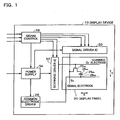
- FIG. 1 schematically shows a display device to which a display driver circuit including a reference voltage generation circuit according to one comparative example is applied.
- a display device (electro-optical device or liquid crystal device in a narrow sense) 10 may include a display panel (liquid crystal panel in a narrow sense) 20.
- the display panel 20 is formed on a glass substrate, for example.
- a plurality of scanning electrodes (gate lines) G 1 to G N (N is an integer equal to or larger than 2) which are arranged in the Y direction and extend in the X direction, and a plurality of signal electrodes (source lines) S 1 to S M (M is an integer equal to or larger than 2) which are arranged in the X direction and extend in the Y direction are disposed on the glass substrate.
- a pixel region (pixel) is provided corresponding to the intersection point between the scanning electrode G n (1 ⁇ n ⁇ N, n is an integer) and the signal electrode S m (1 ⁇ m ⁇ M, m is an integer).
- a thin film transistor (TFT) 22 nm is disposed in the pixel region.
- a gate electrode of the TFT 22 nm is connected with the scanning electrode G n .
- a source electrode of the TFT 22 nm is connected with the signal electrode S m .
- a drain electrode of the TFT 22 nm is connected with a pixel electrode 26 nm of a liquid crystal capacitance (liquid crystal element in a broad sense) 24nm.
- the liquid crystal capacitance 24 nm is formed by sealing a liquid crystal between the pixel electrode 26 nm and a common electrode 28 nm opposite thereto.
- the transmittance of the pixel is changed corresponding to voltage applied between these electrodes.
- a common electrode voltage Vcom is supplied to the common electrode 28 nm .
- the display device 10 may include a signal driver IC 30.
- the display driver circuit in this example may be used as the signal driver IC 30.
- the signal driver IC 30 drives the signal electrodes S 1 to S M of the display panel 20 based on image data.
- the display device 10 may include a scanning driver IC 32.
- the scanning driver IC 32 sequentially drives the scanning electrodes G 1 to G N of the display panel 20 in one vertical scanning period.
- the display device 10 may include a power supply circuit 34.
- the power supply circuit 34 generates voltage necessary for driving the signal electrode and supplies the voltage to the signal driver IC 30.
- the power supply circuit 34 generates voltage necessary for driving the scanning electrode and supplies the voltage to the scanning driver IC 32.
- the power supply circuit 34 generates the common electrode voltage Vcom.
- the display device 10 may include a common electrode driver circuit 36.
- the common electrode voltage Vcom generated by the power supply circuit 34 is supplied to the common electrode driver circuit 36.
- the common electrode driver circuit 36 outputs the common electrode voltage Vcom to the common electrode of the display panel 20.
- the display device 10 may include a signal control circuit 38.
- the signal control circuit 38 controls the signal driver IC 30, the scanning driver IC 32, and the power supply circuit 34 according to the contents set by a host such as a central processing unit (or CPU, not shown). For example, the signal control circuit 38 sets the operation mode, or supplies a vertical synchronization signal or a horizontal synchronization signal generated therein to the signal driver IC 30 and the scanning driver IC 32.
- the signal control circuit 38 controls a polarity inversion timing of the power supply circuit 34.
- the display device 10 includes the power supply circuit 34, the common electrode driver circuit 36, and the signal control circuit 38. However, at least one of these circuits may be provided outside the display device 10.
- the display device 10 may include the host.
- At least either the display driver circuit having a function of the signal driver IC 30 or the scanning electrode driver circuit having a function of the scanning driver IC 32 may be formed on the glass substrate on which the display panel 20 is formed.
- the signal driver IC 30 outputs voltage corresponding to grayscale data to the signal electrode for performing grayscale display based on the grayscale data.
- the signal driver IC 30 gamma-corrects the voltage to be output to the signal electrode based on the grayscale data. Therefore, the signal driver IC 30 includes a reference voltage generation circuit (or a gamma correction circuit, in a narrow sense) for performing gamma correction.
- grayscale characteristics of the display panel 20 differ depending on the structure of the display panel 20 or a liquid crystal material used therefor. Specifically, the relationship between the voltage which should be applied to the liquid crystal and the transmittance of the pixel does not become uniform. Therefore, gamma correction is performed by the reference voltage generation circuit in order to generate an optimum voltage which should be applied to the liquid crystal corresponding to the grayscale data.
- gamma correction multi-valued voltages generated by a resistance ladder are corrected in order to optimize the voltage which is selected and output based on the grayscale data.
- the resistance ratio of the resistance circuits of the resistance ladder is determined so that the voltage specified by the manufacturer or the like of the display panel 20 is generated.
- Gamma correction enables the display panel to be driven by using voltage optimum for the display panel to be driven.
- a reference voltage generation circuit which can be widely used irrespective of the type of display panel to be driven, and a display driver circuit using the same are provided.
- the signal driver IC 30 to which the display driver circuit including the above reference voltage generation circuit is applied is described below.
- FIG. 2 is a block diagram showing the signal driver IC 30 to which the display driver circuit including the reference voltage generation circuit according to one comparative example is applied.
- the signal driver IC 30 includes an input latch circuit 40, a shift register 42, a line latch circuit 44, a latch circuit 46, a reference voltage generation circuit (or a gamma correction circuit, in a narrow sense) 48, a digital/analog converter (DAC, or a voltage select circuit, in a broad sense) 50, and a voltage follower circuit (or a signal electrode driver circuit, in a broad sense) 52.
- the input latch circuit 40 latches the grayscale data consisting of each six bits of RGB signals supplied from the signal control circuit 38 shown in FIG. 1 based on a clock signal CLK, for example.
- the clock signal CLK is supplied from the signal control circuit 38.
- the grayscale data latched by the input latch circuit 40 is sequentially shifted in the shift register 42 based on the clock signal CLK.
- the grayscale data sequentially shifted in the shift register 42 is captured in the line latch circuit 44.
- the grayscale data captured in the line latch circuit 44 is latched by the latch circuit 46 at a timing of a latch pulse signal LP.
- the latch pulse signal LP is input in a horizontal scanning cycle.
- the reference voltage generation circuit 48 outputs multi-valued reference voltages V0 to VY (Y is a positive integer) generated at the divided nodes which are divided by resistance between the power supply voltage (first power supply voltage) V0 on the high potential side and the power supply voltage (second power supply voltage) VSS on the low potential side by using the resistance ratio of the resistance ladder determined so that the grayscale display of the display panel to be driven is optimized.
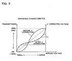
- FIG. 3 is a graph illustrating the principle of gamma correction.
- Grayscale characteristics showing a change in transmittance of the pixel with respect to the voltage applied to the liquid crystal is shown in this figure. If the transmittance of the pixel is indicated by 0% to 100 % (or 100% to 0%), the change in transmittance is generally decreased as the voltage applied to the liquid crystal is decreased or increased. The change in transmittance is increased in a region near the middle of the voltage applied to the liquid crystal.
- transmittance which is gamma-corrected so as to be linearly changed corresponding to the applied voltage can be realized by performing gamma ( ⁇ ) correction so that the change in transmittance is the reverse of the above-described change in transmittance. Therefore, a reference voltage Vy which realizes an optimized transmittance can be generated based on the grayscale data as digital data. Specifically, the resistance ratio of the resistance ladder is determined so that such a reference voltage is generated.
- the multi-valued reference voltages V0 to VY generated by the reference voltage generation circuit 48 shown in FIG. 2 are supplied to the DAC 50.
- the DAC 50 selects one of the multi-valued reference voltages V0 to VY based on the grayscale data supplied from the latch circuit 46, and outputs the selected reference voltage to the voltage follower circuit 52.
- the voltage follower circuit 52 performs impedance transformation and drives the signal electrode based on the voltage supplied from the DAC 50.
- the signal driver IC 30 performs impedance transformation by using the voltage selected from the multi-valued reference voltages based on the grayscale data, and outputs the voltage to each signal electrode.
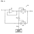
- FIG. 4 schematically shows the voltage follower circuit 52.
- the voltage follower circuit 52 includes an operational amplifier 60 and first and second switch elements Q1 and Q2.
- the operational amplifier 60 is voltage follower connected. Specifically, an output terminal of the operational amplifier 60 is connected with an inverting input terminal of the operational amplifier 60, whereby negative feedback is formed.
- a reference voltage Vin selected by the DAC 50 shown in FIG. 2 is input to a noninverting input terminal of the operational amplifier 60.
- the output terminal of the operational amplifier 60 is connected with the signal electrode to which a drive voltage Vout is output through the first switch element Q1.
- the signal electrode is also connected with the noninverting input terminal of the operational amplifier 60 through the second switch element Q2.
- a control signal generation circuit 62 generates a control signal VFcnt for ON-OFF controlling the first and second switch elements Q1 and Q2.
- the control signal generation circuit 62 may be provided for each unit of one or more signal electrodes.
- the second switch element Q2 is ON-OFF controlled by the control signal VFcnt.
- the first switch element Q1 is ON-OFF controlled by an output signal of an inverter circuit INV1 to which the control signal VFcnt is input.
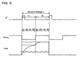
- FIG. 5 shows an example of the operation timing of the voltage follower circuit 52.
- the logic level of the control signal VFcnt generated by the control signal generation circuit 62 is changed between a former period (a given first period of a drive period) t1 and a latter period t2 of a select period (or a drive period) t specified by the latch pulse signal LP. Specifically, when the logic level of the control signal VFcnt becomes "L" in the former period t1, the first switch element Q1 is turned ON and the second switch element Q2 is turned OFF. When the logic level of the control signal VFcnt becomes "H” in the latter period t2, the first switch element Q1 is turned OFF and the second switch element Q2 is turned ON. Therefore, in the former period t1 of the select period t, the signal electrode is driven after impedance transformation by the voltage follower connected operational amplifier 60. In the latter period t2, the signal electrode is driven by using the reference voltage output from the DAC 50.
- the reference voltage generation circuit 48 shown in FIG. 2 is formed so that only some of the resistance circuits can be variably controlled without making all the resistance circuits of the resistance ladder variable, taking grayscale characteristics of a display panel to be driven into consideration. This enables the circuit scale of the resistance ladder, interconnection of control lines, and the control of the resistance ladder to be simplified. In particular, since an increase in the number of grayscale levels involves expectation of an increase in the number of reference voltages to be generated, it is preferable that the reference voltage generation circuit can be multi-purposely used without increasing the circuit size of the resistance ladder circuit as much as possible and irrespective of the type of display panel.
- the reference voltage generation circuit 48 variably controls the resistance ladder based on a given command from the user or a variable control signal input through an external input terminal instead of switching interconnects by changing a mask pattern or the like. This enables the signal driver IC 30 to be widely used irrespective of the type of display panel.
- the reference voltage generation circuit 48 is described below in detail.
- FIG. 6 schematically shows the reference voltage generation circuit 48 according to one comparative example.
- the DAC 50 and the voltage follower circuit 52 are also illustrated in this figure.
- the reference voltage generation circuit 48 outputs the multi-valued reference voltages V0 to VY by the resistance ladder connected between the first power supply line to which the power supply voltage (first power supply voltage) V0 on the high potential side is supplied and the second power supply line to which the power supply voltage (second power supply voltage) VSS on the low potential side is supplied.
- the reference voltage generation circuit 48 includes first to third resistance ladder circuits 70, 72, and 74.
- the first resistance ladder circuit 70 includes at least one variable resistance circuit in which the resistance value between both ends is variable, and outputs multi-valued voltages.
- the second resistance ladder circuit 72 has a plurality of series-connected resistance circuits each having a fixed resistance value, and outputs a plurality of voltages.
- the third resistance ladder circuit 74 includes at least one variable resistance circuit in which the resistance value between both ends is variable, and outputs multi-valued voltages.
- the first to third resistance ladder circuits 70, 72, and 74 are connected in series between the first and second power supply lines.
- one end of the first resistance ladder circuit 70 is connected with the first power supply line.
- the other end of the first resistance ladder circuit 70 is connected with one end of the second resistance ladder circuit 72.
- the other end of the second resistance ladder circuit 72 is connected with one end of the third resistance ladder circuit 74.
- the other end of the third resistance ladder circuit 74 is connected with the second power supply line.
- the first resistance ladder circuit 70 outputs voltages generated between both ends of each resistance circuit in the resistance ladder as the multi-valued reference voltages.
- the second resistance ladder circuit 72 outputs voltages across the resistance circuits of the resistance ladder as the multi-valued reference voltages.
- the third resistance ladder circuit 74 outputs voltages across the resistance circuits of the resistance ladder as the multi-valued reference voltages.
- the resistance value of the variable resistance circuit of the first resistance ladder circuit 70 is variably controlled based on a first command specified by the user or a first variable control signal input through a given external input terminal, for example.
- the resistance value of the variable resistance circuit of the third resistance ladder circuit 74 is variably controlled based on a second command specified by the user or a second variable control signal input through a given external input terminal, for example.
- the first and third resistance ladder circuits 70 and 74 may include a resistance circuit having a fixed resistance value, or may be formed only of the variable resistance circuits.
- the first and third resistance ladder circuits 70 and 74 include at least one variable resistance circuit.
- the variable resistance circuit may be realized by a resistance element or a resistance element and a switch element, for example.
- the first and second commands may be the same command or separately specified.
- the first and second variable control signals may be the same signal or separately input.
- the reference voltage generation circuit 48 has a configuration in which only the resistance circuits for generating the reference voltages close to the first and the second power supply voltages are variably controlled in the resistance ladder connected between the first and second power supply lines. This eliminates the need to variably control all the resistance circuits of the resistance ladder, whereby the control is facilitated and an increase in circuit scale can be prevented.
- the multi-valued reference voltages V0 to VY generated by the reference voltage generation circuit 48 are supplied to the DAC 50.
- the DAC 50 includes switch circuits provided for each reference voltage output node. Each switch circuit is alternatively turned ON based on the grayscale data supplied from the latch circuit 46 shown in FIG. 2 .
- the DAC 50 outputs the select voltage to the voltage follower circuit 52 as the output voltage Vin.
- FIG. 7 is a graph illustrating grayscale characteristics.
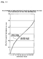
- grayscale characteristics of a display panel differ depending on the structure of the display panel or a liquid crystal material used therefor. Therefore, it is known that the relationship between the voltage which should be applied to the liquid crystal and the transmittance of the pixel does not become constant. Taking a first liquid crystal panel designed for a power supply voltage of 5 V and a second liquid crystal panel designed for a power supply voltage of 3 V as examples, the range of the applied voltage at which the liquid crystal panel is operated in an active region in which the change in transmittance of the pixel is large differs between the first and second liquid crystal panels, as shown in FIG. 7 .
- the resistance ratio of the resistance ladder used herein refers to a ratio of the resistance value of each resistance circuit of the resistance ladder to the total resistance value of the resistance ladder connected in series between the first and second power supply lines.
- FIG. 8 shows reference voltages optimized for grayscale values in the first and second liquid crystal panels.
- Reference voltages optimized for 64 grayscale values are indicated by relative value ratios based on the power supply voltage.
- the relative value of the reference voltage is "100" when the grayscale value is maximum.
- the corrected reference voltages differs depending on the type of liquid crystal panel.
- the inventor of the present invention has analyzed the resistance value ratio and obtained the following results.
- the meaning of the resistance value ratio is as follows.
- the resistance value ratio refers to the ratio of the first resistance value to the second resistance value.
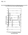
- FIG. 9 shows the relationship between a grayscale value and a resistance value ratio of the first and second liquid crystal panels.
- resistance value ratios necessary for generating the reference voltages for 64 grayscale levels are shown in this graph.
- the resistance value ratios are increased in sections 80 and 82 in which the reference voltages close to the power supply voltage on the high potential side and the power supply voltage on the low potential side are generated.
- the resistance value ratios in a half tone section 84 are approximately "1". In the case where the resistance value ratio is approximately "1", the resistance values for generating the reference voltages corresponding to the grayscale value are equal.
- the resistance values for generating the reference voltages in the half tone become substantially "1", as shown in FIG. 10 . Therefore, the resistance circuits for generating the reference voltages in the half tone can be shared.
- a reference voltage generation circuit capable of performing gamma correction optimum for different types of liquid crystal panels can be provided by adjusting only the resistance values of several (four, for example) resistance circuits disposed close to the power supply voltages on the high and low potential sides of the resistance ladder. Specifically, it is unnecessary to variably control all the resistance circuits of the resistance ladder.
- the reference voltage generation circuit 48 only the first and third resistance ladder circuits 70 and 74 are variably controlled, and the second resistance ladder circuit 72 for generating the reference voltages in the half tone is formed only of the resistance circuits having a fixed resistance value.
- each resistance circuit of the second resistance ladder circuit 72 is two or less, a general-purpose reference voltage generation circuit can be provided without impairing the grayscale characteristics.
- FIG. 12 shows an example of the signal driver IC 30 to which the reference voltage generation circuit 48 is applied.
- the reference voltage generation circuit 48 is shared to drive M signal electrodes in this figure. Specifically, the DACs 50-1 to 50-M and the voltage follower circuits 52-1 to 52-M are respectively provided for the M signal electrodes S 1 to S M .
- the DACs 50-1 to 50-M select one of the multi-valued reference voltages based on the grayscale data corresponding to each signal electrode.
- the multi-valued reference voltages supplied to the DACs 50-1 to 50-M are generated by the reference voltage generation circuit 48.
- the reference voltage generation circuit 48 includes the first to third resistance ladder circuits 70, 72, and 74. In the first and third resistance ladder circuits 70 and 74, the resistance values of the resistance circuits of the resistance ladder are variably controlled by the command from the user or the variable control signal input through the external input terminal. This configuration makes the effect of preventing an increase in circuit scale by the reference voltage generation circuit 48 significant, even if the number of signal electrodes is increased.
- a region between given transmittances tr1 and tr2 in which the change in transmittance is large is referred to as an active region, and regions other than the active region are referred to as first and second non-active regions.
- the active region is a region in which the voltage corresponding to the grayscale value in the half tone is applied.
- the first non-active region is a region in which the transmittance is changed when a higher voltage is applied to the liquid crystal
- the second non-active region is a region in which the transmittance is changed when a lower voltage is applied to the liquid crystal.
- an applied voltage for obtaining the transmittance tr2 is VA
- the difference in voltage between the first and the second power supply voltages is VDIF
- the resistance values of the variable resistance circuits which are variably controlled in the first and third resistance ladder circuits 70 and 74 are increased as (VDIF-VA) /VDIF becomes larger
- the resistance values of the variable resistance circuits which are variably controlled in the first and third resistance ladder circuits 70 and 74 are decreased as (VDIF-VA)/VDIF becomes smaller.
- the resistance values of the variable resistance circuits which are variably controlled in the first and third resistance ladder circuits 70 and 74 in the first liquid crystal panel shown in FIG. 8 are set larger than the resistance values of the variable resistance circuits which are variably controlled in the first and third resistance ladder circuits 70 and 74 in the second liquid crystal panel.
- the resistance value ratio shown in FIG. 9 be two or less in the active region.
- the second resistance ladder circuit 72 be formed so that the resistance circuits having a resistance value ratio of two or less are connected in series.
- the variable resistance circuits of the first and third resistance ladder circuits 70 and 74 which generate the reference voltages corresponding to grayscale values on both ends are variably controlled as described above.
- the signal driver IC 30 including the reference voltage generation circuit 48 shown in FIG. 6 can be widely used irrespective of the display panel to be driven by variably controlling the variable resistance circuits as described above.
- the first and third resistance ladder circuits 70 and 74 which are variably controlled in the reference voltage generation circuit 48 as described above may have the following configuration.
- the following description illustrates the first resistance ladder circuit 70, but the third resistance ladder circuit 74 may have the same configuration as the first resistance ladder circuit 70.
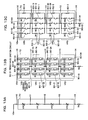
- FIGS. 13A to 13C A first example of the first resistance ladder circuit 70 is shown in FIGS. 13A to 13C .
- the first resistance ladder circuit 70 includes variable resistance circuits VR0 to VR3 connected in series, as shown in FIG. 13A .
- variable resistance circuit may be formed by parallelly connecting resistance switch circuits in which a switch circuit (switch element) and a resistance circuit (resistance element) are connected in series.
- the resistance switch circuits connected in parallel are controlled so that at least one of the switch circuits is turned ON based on the command or the variable control signal input through the external input terminal.
- variable resistance circuit VR0 may be formed by connecting resistance switch circuits 90-01 to 90-04 in parallel.
- the variable resistance circuit VR1 may be formed by connecting resistance switch circuits 90-11 to 90-14 in parallel.
- the variable resistance circuit VR2 may be formed by connecting resistance switch circuits 90-21 to 90-24 in parallel.
- the variable resistance circuit VR3 may be formed by connecting resistance switch circuits 90-31 to 90-34 in parallel.
- a resistance circuit may be further connected in parallel with the resistance switch circuits which are connected in parallel in the variable resistance circuit.
- variable resistance circuit VR0 may be formed by connecting a resistance circuit 92-0 in parallel with the resistance switch circuits 90-01 to 90-04.
- the variable resistance circuit VR1 may be formed by connecting a resistance circuit 92-1 in parallel with the resistance switch circuits 90-11 to 90-14.
- the variable resistance circuit VR2 may be formed by connecting a resistance circuit 92-2 in parallel with the resistance switch circuits 90-21 to 90-24.
- the variable resistance circuit VR3 may be formed by connecting a resistance circuit 92-3 in parallel with the resistance switch circuits 90-31 to 90-34.
- the switch circuit of each resistance switch circuit is ON-OFF controlled based on the command or the variable control signal input through the external input terminal.
- a second example of the first resistance ladder circuit 70 is shown in FIG. 14 .
- the first resistance ladder circuit 70 includes the variable resistance circuits VR0 to VR3 connected in series similarly to FIG. 13A .
- the variable resistance circuit may be formed by connecting resistance switch circuits in series in which a resistance circuit and a switch circuit are connected in parallel, as shown in FIG. 14 .
- the switch element of the resistance switch circuit is ON-OFF controlled based on the command or the variable control signal input through the external input terminal.
- variable resistance circuit VR0 may be formed by connecting resistance switch circuits 94-01 to 94-04 in series.
- the variable resistance circuit VR1 may be formed by connecting resistance switch circuits 94-11 to 94-14 in series.
- the variable resistance circuit VR2 may be formed by connecting resistance switch circuits 94-21 to 94-24 in series.
- the variable resistance circuit VR3 may be formed by connecting resistance switch circuits 94-31 to 94-34 in series.
- the switch circuit of each resistance switch circuit is ON-OFF controlled based on the command or the variable control signal input through the external input terminal.
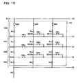
- a third example of the first resistance ladder circuit 70 is shown in FIG. 15 .
- the first resistance ladder circuit 70 includes the variable resistance circuits VR0 to VR3 connected in series similarly to FIG. 13A .
- variable resistance circuit VR0 a switch circuit (switch element) SWA and a resistance circuit R 01 connected in series are inserted between the first power supply line and the divided node ND1.
- a switch circuit SW 11 is inserted between the divided node ND1 and the output node of the reference voltage V1.
- a switch circuit SWB and a resistance circuit R 02 connected in series are inserted between the first power supply line and a node ND1B.
- a switch circuit SW 12 is inserted between the node ND1B and the output node of the reference voltage V1.
- a switch circuit SWC and a resistance circuit R 03 connected in series are inserted between the first power supply line and a node ND1C.
- a switch circuit SW 13 is inserted between the node ND1C and the output node of the reference voltage V1.
- variable resistance circuit VR1 a resistance circuit R 11 is inserted between the divided node ND1 and the divided node ND2.
- a switch circuit SW 21 is inserted between the divided node ND2 and the output node of the reference voltage V2.
- a resistance circuit R 12 is inserted between the node ND1B and a node ND2B.
- a switch circuit SW 22 is inserted between the node ND2B and the output node of the reference voltage V2.
- a resistance circuit R 13 is inserted between the node ND1C and a node ND2C.
- a switch circuit SW 23 is inserted between the node ND2C and the output node of the reference voltage V2.
- variable resistance circuit VR2 a resistance circuit R 21 is inserted between the divided node ND2 and the divided node ND3.
- a switch circuit SW 31 is inserted between the divided node ND3 and the output node of the reference voltage V3.
- a resistance circuit R 22 is inserted between the node ND2B and a node ND3B.
- a switch circuit SW 32 is inserted between the node ND3B and the output node of the reference voltage V3.
- a resistance circuit R 23 is inserted between the node ND2C and a node ND3C.
- a switch circuit SW 33 is inserted between the node ND3C and the output node of the reference voltage V3.
- variable resistance circuit VR3 a resistance circuit R 31 is inserted between the divided node ND3 and the output node of the reference voltage V4.
- a resistance circuit R 32 is inserted between the node ND3B and the output node of the reference voltage V4.
- a resistance circuit R 33 is inserted between the node ND3C and the output node of the reference voltage V4.
- the switch circuits SWA, SWB, SWC, SW 11 to SW 13 , SW 21 to SW 23 , and SW 31 to SW 33 are ON-OFF controlled based on the command or the variable control signal input through the external input terminal.
- the settable resistance value of the variable resistance circuit of the resistance ladder can be further diversified, a signal driver IC including a reference voltage generation circuit which can be optimized for various display panels can be provided.
- FIG. 16 A fourth example of the first resistance ladder circuit 70 according to one embodiment of the present invention is shown in FIG. 16 .
- the first resistance ladder circuit 70 includes the variable resistance circuits VR0 to VR3 connected in series similarly to FIG. 13A .
- variable resistance circuit VR0 a resistance circuit R0 is inserted between the first power supply line and the divided node ND1.
- a voltage follower circuit 96-1 is inserted between the divided node ND1 and the output node of the reference voltage V1.
- the voltage follower circuit 96-1 has the same configuration as the voltage follower circuit shown in FIG. 4 .
- Each switch circuit of the voltage follower circuit 96-1 is ON-OFF controlled by control signals cnt0 and cnt1.
- variable resistance circuit VR1 a resistance circuit R1 is inserted between the divided node ND1 and the divided node ND2.
- a voltage follower circuit 96-2 is inserted between the divided node ND2 and the output node of the reference voltage V2.
- the voltage follower circuit 96-2 has the same configuration as the voltage follower circuit shown in FIG. 4 .
- Each switch circuit of the voltage follower circuit 96-2 is ON-OFF controlled by the control signals cnt0 and cnt1.
- variable resistance circuit VR2 a resistance circuit R2 is inserted between the divided node ND2 and the divided node ND3.
- a voltage follower circuit 96-3 is inserted between the divided node ND3 and the output node of the reference voltage V3.
- the voltage follower circuit 96-3 has the same configuration as the voltage follower circuit shown in FIG. 4 .
- Each switch circuit of the voltage follower circuit 96-3 is ON-OFF controlled by the control signals cnt0 and cnt1.
- variable resistance circuit VR3 a resistance circuit R3 is inserted between the divided node ND3 and the output node of the reference voltage V4.
- an operational amplifier circuit 98 with an offset is inserted between an output terminal of a voltage follower connected operational amplifier of the voltage follower circuit 96-3 and the output node of the reference voltage V4.
- the operation of the operational amplifier circuit 98 is controlled by the control signal cnt1 (operating current is controlled by the control signal cnt1).
- a resistance element (resistance circuit R2, for example) is inserted between the i-th (1 ⁇ i ⁇ R, i is an integer) divided node (divided node ND3, for example) for generating the i-th reference voltage (reference voltage V3, for example) and the (i-1)th divided node (divided node ND2, for example) for generating the (i-1)th reference voltage, among the first to R-th reference voltages (R is an integer equal to or larger than 2).
- the first resistance ladder circuit 70 includes a first voltage follower connected operational amplifier (operational amplifier of the voltage follower circuit 96-3, for example) of which an input terminal is connected with the i-th divided node, a first switch element (first switch element of the voltage follower circuit 96-3, for example) inserted between the output node of the i-th reference voltage and the output of the first operational amplifier circuit, and a second switch element (second switch element of the voltage follower circuit 96-3, for example) inserted between the output node of the i-th reference voltage and the i-th divided node.
- first voltage follower connected operational amplifier operational amplifier of the voltage follower circuit 96-3, for example
- first switch element first switch element of the voltage follower circuit 96-3, for example
- second switch element of the voltage follower circuit 96-3 for example
- a second operational amplifier circuit (operational amplifier circuit 98, for example) is inserted between the output of the first operational amplifier (operational amplifier of the voltage follower circuit 96-3, for example) and the output node of the (i+1)th reference voltage.
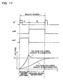
- FIG. 17 shows an example of the control timing of the first resistance ladder circuit 70 shown in FIG. 16 .
- the logic levels of the control signals cnt0 and cnt1 are changed between the former period (first given period of drive period) t1 and the latter period t2 of the select period (drive period) specified by the latch pulse signal LP, for example. Specifically, when the logic level of the control signal cnt0 becomes “L” and the logic level of the control signal cnt1 becomes "H” in the former period t1, the voltage follower connected operational amplifier drives the output node of the reference voltage V1.
- the drive voltage Vout can be raised at high speed by the voltage follower connected operational amplifier having high drive capability in the former period t1 necessary for charging the liquid crystal capacitance, interconnect capacitance, and the like, and the drive voltage can be output by the resistance circuit R0 in the latter period t2 in which high drive capability is unnecessary, as shown in FIG. 17 . Therefore, since the impedance transformation can be performed by the voltage follower circuit, effects the same as in the first to third examples can be obtained.
- variable resistance circuit VR3 the reference voltage V3 to which an offset voltage is added by the operational amplifier circuit 98 is output as the reference voltage V4 in the former period t1 of the select period t.
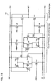
- FIG. 18 is a detailed circuit diagram showing an example of the operational amplifier circuit 98.
- the operational amplifier circuit 98 includes a differential amplifier section 100 and an output section 102.
- the differential amplifier section 100 includes first and second differential amplifier sections 104 and 106.
- the first differential amplifier section 104 utilizes current flowing between a drain and a source of an n-type MOS transistor Trn1 (n-type MOS transistor Trnx (x is an integer) is hereinafter abbreviated as "transistor Trnx”) to which a reference signal VREFN is applied at a gate electrode as a current source.
- the current source is connected with source terminals of transistors Trn2 to Trn4.
- An output signal OUT of the operational amplifier circuit 98 is applied to gate electrodes of the transistors Trn2 and Trn3.
- An input signal IN is applied to a gate electrode of the transistor Trn4.
- the drain terminals of the transistors Trn2 to Trn4 are connected with drain terminals of p-type MOS transistors Trp1 (p-type MOS transistor Trpy (y is an integer) is hereinafter abbreviated as "transistor Trpy”) and Trp2 having a current mirror structure.
- Transistor Trpy p-type MOS transistor Trpy (y is an integer) is hereinafter abbreviated as "transistor Trpy"
- Trp2 p-type MOS transistor Trpy (y is an integer) is hereinafter abbreviated as "transistor Trpy") and Trp2 having a current mirror structure.
- Gate electrodes of the transistors Trp1 and Trp2 are connected with drain terminals of the transistors Trn2 and Trn3.
- a differential output signal SO1 is output from the drain terminal of the transistor Trp2.
- the second differential amplifier section 106 utilizes current flowing between a drain and a source of a transistor Trp3 to which a reference signal VREFP is applied at a gate electrode as a current source.
- the current source is connected with source terminals of transistors Trp4 to Trp6.
- the output signal OUT of the operational amplifier circuit 98 is applied to gate electrodes of the transistors Trp4 and Trp5.
- the input signal IN is applied to a gate electrode of the transistor Trp6.
- the drain terminals of the transistors Trp4 to Trp6 are connected with drain terminals of transistors Trn5 and Trn6 having a current mirror structure.
- Gate electrodes of the transistors Trn5 and Trn6 are connected with the drain terminals of the transistors Trp4 and Trp5.
- a differential output signal SO2 is output from the drain terminal of the transistor Trn6.
- the output section 102 includes transistors Trp7 and Trn7 connected in series between the power supply voltage VDD and the ground power supply voltage VSS.
- the differential output signal SO1 is applied to a gate electrode of the transistor Trp7.
- the differential output signal SO2 is applied to a gate electrode of the transistor Trn7.
- the output signal OUT is output from drain terminals of the transistors Trp7 and Trn7.
- the gate electrode of the transistor Trp7 is connected with a drain terminal of a transistor Trp8.
- a source terminal of the transistor Trp8 is connected with the power supply voltage VDD.
- An enable signal ENB is applied to a gate electrode of the transistor Trp8.
- the gate electrode of the transistor Trn7 is connected with a drain terminal of a transistor Trn8.
- a source terminal of the transistor Trn8 is connected with the ground power supply voltage VSS.
- An inverted enable signal XENB is applied to a gate electrode of the transistor Trn8.
- the operational amplifier circuit 98 having the above-described configuration makes the reference signals VREFN and VREFP, the enable signal ENB, and the inverted enable signal XENB operate, and outputs the output signal OUT which is a voltage obtained by adding an offset voltage to the input signal IN, as shown in FIG. 19 .
- the control signal cnt1 shown in FIGS. 16 and 17 may be used as the reference signal VREFN and the enable signal ENB.
- a signal obtained by inverting the control signal cnt1 may be used as the reference signal VREFP and the inverted enable signal XENB.
- the differential output signal SO1 is applied to the gate electrode of the transistor Trp7.
- the differential output signal SO2 is applied to the gate electrode of the transistor Trn7.
- the output section 102 outputs the output signal OUT which is the input signal IN to which an offset corresponding to the drive capability of the transistors which make up the differential pair is added.
- the power supply voltage VDD is applied to the gate electrode of the transistor Trp7 through the transistor Trp8.
- the ground power supply voltage VSS is applied to the gate electrode of the transistor Trn7 through the transistor Trn8.
- the output section 102 puts its output in a high impedance state. Since the current flowing through the current source can be limited or terminated by the reference signals VREFN and VREFP, the operating current can be prevented from flowing in a period in which the operation is unnecessary.
- the resistance value of the variable resistance circuit can be variably controlled by using impedance transformation by the voltage follower circuit, whereby a general-purpose reference voltage generation circuit irrespective of the type of display panel can be formed.
- variable resistance circuits VR0 to VR3 are variably controlled by the control signals cnt0 and cnt1.
- the present invention is not limited thereto.
- the variable resistance circuits VR0 to VR3 may be variably controlled by different control signals.
- the above embodiments are described taking the liquid crystal device including a liquid crystal panel using TFTs as an example, but the present invention is not limited thereto.
- the reference voltage generated by the reference voltage generation circuit 48 may be changed into current by a given current conversion circuit and supplied to a current driven type element. This enables the present invention to be applied to a signal driver IC which drives an organic EL panel including organic EL elements provided corresponding to pixels specified by signal electrodes and scanning electrodes, for example.
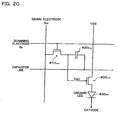
- FIG. 20 is a circuit diagram showing an example of a two-transistor pixel circuit in an organic EL panel driven by such a signal driver IC.
- the organic EL panel includes a drive TFT 800 nm , a switch TFT 810 nm , a storage capacitor 820 nm , and an organic LED 830 nm at an intersection point between a signal electrode S m and a scanning electrode G n .
- the drive TFT 800 nm is formed by a p-type transistor.
- the drive TFT 800 nm and the organic LED 830 nm are connected in series with a power supply line.
- the switch TFT 810 nm is inserted between a gate electrode of the drive TFT 800 nm and the signal electrode S m .
- a gate electrode of the switch TFT 810 nm is connected with the scanning electrode G n .
- the storage capacitor 820 nm is inserted between the gate electrode of the drive TFT 800 nm and a capacitor line.
- the gate voltage Vgs corresponding to the voltage of the signal electrode S m is held by the storage capacitor 820 nm , for example, in the case where current corresponding to the gate voltage Vgs is caused to flow through the organic LED 830 nm in one frame period, a pixel which continues to shine during the frame can be realized.
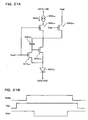
- FIG. 21A shows an example of a four-transistor pixel circuit in an organic EL panel driven by the signal driver IC.
- FIG. 21B shows an example of the display control timing of the pixel circuit.
- the organic EL panel includes a drive TFT 900 nm , a switch TFT 910 nm , a storage capacitor 920 nm , and an organic LED 930 nm .
- a constant current Idata from a constant current source 950 nm is supplied to the pixel through a p-type TFT 940 nm as a switch element instead of a constant voltage, and the storage capacitor 920 nm and the drive TFT 900 nm are connected with the power supply line through a p-type TFT 960 nm as a switch element.
- the power supply line is disconnected by allowing the p-type TFT 960 nm to be turned OFF by a gate voltage Vgp, and the constant current Idata from the constant current source 950 nm is caused to flow through the drive TFT 900 nm by allowing the p-type TFT 940 nm and the switch TFT 910 nm to be turned ON by a gate voltage Vsel.
- Voltage corresponding to the constant current Idata is held by the storage capacitor 920 nm until the current flowing through the drive TFT 900 nm becomes stable.
- the p-type TFT 940 nm and the switch TFT 910 nm are turned OFF by the gate voltage Vsel and the p-type TFT 960 nm is turned ON by the gate voltage Vgp, whereby the power supply line is electrically connected with the drive TFT 900 nm and the organic LED 930 nm .
- Current almost equal to or in an amount corresponding to the constant current Idata is supplied to the organic LED 930 nm by the voltage held by the storage capacitor 920 nm .
- the scanning electrode may be used as an electrode to which the gate voltage Vsel is applied, and the signal electrode may be used as a data line.
- the organic LED may have a structure in which a light-emitting layer is provided on a transparent anode (ITO) and a metal cathode is provided on the light-emitting layer, or a structure in which a light-emitting layer, a light-transmitting cathode, and a transparent seal are provided on a metal anode.
- ITO transparent anode
- the element structure of the organic LED is not limited.
- a signal driver IC which is widely used for organic EL panels can be provided by forming a signal driver IC which drives an organic EL panel including organic EL elements as described above.
Landscapes
- Engineering & Computer Science (AREA)
- Theoretical Computer Science (AREA)
- Physics & Mathematics (AREA)
- Computer Hardware Design (AREA)
- General Physics & Mathematics (AREA)
- Crystallography & Structural Chemistry (AREA)
- Chemical & Material Sciences (AREA)
- Liquid Crystal Display Device Control (AREA)
- Control Of Indicators Other Than Cathode Ray Tubes (AREA)
- Liquid Crystal (AREA)
- Control Of El Displays (AREA)
- Control Of Electrical Variables (AREA)
- Measurement Of Current Or Voltage (AREA)
Applications Claiming Priority (2)
| Application Number | Priority Date | Filing Date | Title |
|---|---|---|---|
| JP2002032677A JP3661650B2 (ja) | 2002-02-08 | 2002-02-08 | 基準電圧発生回路、表示駆動回路及び表示装置 |
| JP2002032677 | 2002-02-08 |
Publications (2)
| Publication Number | Publication Date |
|---|---|
| EP1335347A1 EP1335347A1 (en) | 2003-08-13 |
| EP1335347B1 true EP1335347B1 (en) | 2009-04-29 |
Family
ID=27606543
Family Applications (1)
| Application Number | Title | Priority Date | Filing Date |
|---|---|---|---|
| EP03002553A Expired - Lifetime EP1335347B1 (en) | 2002-02-08 | 2003-02-06 | Reference voltage generation circuit and method, display driver circuit and liquid crystal display device |
Country Status (8)
| Country | Link |
|---|---|
| US (1) | US7071669B2 (ja) |
| EP (1) | EP1335347B1 (ja) |
| JP (1) | JP3661650B2 (ja) |
| KR (1) | KR100536962B1 (ja) |
| CN (1) | CN1254783C (ja) |
| AT (1) | ATE430357T1 (ja) |
| DE (1) | DE60327382D1 (ja) |
| TW (1) | TWI257600B (ja) |
Families Citing this family (55)
| Publication number | Priority date | Publication date | Assignee | Title |
|---|---|---|---|---|
| KR100798309B1 (ko) * | 2001-06-22 | 2008-01-28 | 엘지.필립스 엘시디 주식회사 | 액티브 매트릭스 유기 엘이디 구동회로 |
| KR100878222B1 (ko) * | 2001-07-03 | 2009-01-13 | 삼성전자주식회사 | 액정 표시 장치용 전원 공급 장치 |
| KR100520383B1 (ko) * | 2003-03-18 | 2005-10-11 | 비오이 하이디스 테크놀로지 주식회사 | 액정표시장치의 기준전압 발생회로 |
| JP4009238B2 (ja) * | 2003-09-11 | 2007-11-14 | 松下電器産業株式会社 | 電流駆動装置及び表示装置 |
| JP3922261B2 (ja) * | 2004-03-08 | 2007-05-30 | セイコーエプソン株式会社 | データドライバ及び表示装置 |
| JP4847702B2 (ja) * | 2004-03-16 | 2011-12-28 | ルネサスエレクトロニクス株式会社 | 表示装置の駆動回路 |
| JP2005266346A (ja) | 2004-03-18 | 2005-09-29 | Seiko Epson Corp | 基準電圧発生回路、データドライバ、表示装置及び電子機器 |
| EP1583070A1 (en) * | 2004-03-30 | 2005-10-05 | STMicroelectronics S.r.l. | Method for designing a structure for driving display devices |
| KR100646996B1 (ko) * | 2004-06-16 | 2006-11-23 | 삼성에스디아이 주식회사 | 유기 발광 표시 장치 및 그 제어 방법 |
| TWI238374B (en) * | 2004-06-17 | 2005-08-21 | Au Optronics Corp | Organic light emitting diode display, display luminance compensating device thereof, and compensating method thereof |
| JP4049140B2 (ja) * | 2004-09-03 | 2008-02-20 | セイコーエプソン株式会社 | インピーダンス変換回路、駆動回路及び制御方法 |
| JP4367308B2 (ja) | 2004-10-08 | 2009-11-18 | セイコーエプソン株式会社 | 表示ドライバ、電気光学装置、電子機器及びガンマ補正方法 |
| CN100395816C (zh) * | 2005-01-06 | 2008-06-18 | 鸿富锦精密工业(深圳)有限公司 | 液晶显示器微处理器的代码共用系统 |
| JP4442455B2 (ja) * | 2005-02-17 | 2010-03-31 | セイコーエプソン株式会社 | 基準電圧選択回路、基準電圧発生回路、表示ドライバ、電気光学装置及び電子機器 |
| JP2006227272A (ja) * | 2005-02-17 | 2006-08-31 | Seiko Epson Corp | 基準電圧発生回路、表示ドライバ、電気光学装置及び電子機器 |
| JP2006243232A (ja) * | 2005-03-02 | 2006-09-14 | Seiko Epson Corp | 基準電圧発生回路、表示ドライバ、電気光学装置及び電子機器 |
| JP4810840B2 (ja) * | 2005-03-02 | 2011-11-09 | セイコーエプソン株式会社 | 基準電圧発生回路、表示ドライバ、電気光学装置及び電子機器 |
| JP2006285018A (ja) | 2005-04-01 | 2006-10-19 | Matsushita Electric Ind Co Ltd | 液晶駆動装置および液晶表示装置,液晶駆動方法 |
| US20060232579A1 (en) * | 2005-04-14 | 2006-10-19 | Himax Technologies, Inc. | WOA panel architecture |
| US7379004B2 (en) * | 2006-01-27 | 2008-05-27 | Hannstar Display Corp. | Driving circuit and method for increasing effective bits of source drivers |
| JP4572170B2 (ja) * | 2006-01-30 | 2010-10-27 | Okiセミコンダクタ株式会社 | 出力回路及びこれを用いた表示装置 |
| KR100748319B1 (ko) | 2006-03-29 | 2007-08-09 | 삼성에스디아이 주식회사 | 유기발광표시장치 및 그의 구동방법 |
| TWI354976B (en) * | 2006-04-19 | 2011-12-21 | Au Optronics Corp | Voltage level shifter |
| US20090174372A1 (en) * | 2006-05-24 | 2009-07-09 | Kazuhiro Maeda | Analog Output Circuit, Data Signal Line Driving Circuit, Display, and Potential Writing Method |
| JP4833758B2 (ja) * | 2006-07-21 | 2011-12-07 | Okiセミコンダクタ株式会社 | 駆動回路 |
| JP4773928B2 (ja) | 2006-11-16 | 2011-09-14 | セイコーエプソン株式会社 | ソースドライバ、電気光学装置及び電子機器 |
| TWI383349B (zh) * | 2007-02-16 | 2013-01-21 | Chimei Innolux Corp | 參考電壓產生電路、顯示面板及顯示裝置 |
| JP5374867B2 (ja) * | 2007-02-23 | 2013-12-25 | セイコーエプソン株式会社 | ソースドライバ、電気光学装置、投写型表示装置及び電子機器 |
| JP2008233864A (ja) * | 2007-02-23 | 2008-10-02 | Seiko Epson Corp | ソースドライバ、電気光学装置、投写型表示装置及び電子機器 |
| JP4493681B2 (ja) * | 2007-05-17 | 2010-06-30 | Okiセミコンダクタ株式会社 | 液晶駆動装置 |
| JP2009003243A (ja) | 2007-06-22 | 2009-01-08 | Seiko Epson Corp | 基準電圧選択回路、表示ドライバ、電気光学装置及び電子機器 |
| JP4536759B2 (ja) * | 2007-08-10 | 2010-09-01 | ティーピーオー ディスプレイズ コーポレイション | 変換回路 |
| JP4472737B2 (ja) * | 2007-08-31 | 2010-06-02 | Okiセミコンダクタ株式会社 | 半導体装置、半導体素子及び基板 |
| JP4540697B2 (ja) | 2007-08-31 | 2010-09-08 | Okiセミコンダクタ株式会社 | 半導体装置 |
| JP4498400B2 (ja) * | 2007-09-14 | 2010-07-07 | Okiセミコンダクタ株式会社 | トリミング回路 |
| JP4627773B2 (ja) * | 2007-10-16 | 2011-02-09 | Okiセミコンダクタ株式会社 | 駆動回路装置 |
| TWI415089B (zh) * | 2009-03-05 | 2013-11-11 | Raydium Semiconductor Corp | 用以驅動液晶顯示面板之過載驅動裝置 |
| JP5360684B2 (ja) * | 2009-04-01 | 2013-12-04 | セイコーエプソン株式会社 | 発光装置、電子機器および画素回路の駆動方法 |
| US8143923B2 (en) * | 2009-12-07 | 2012-03-27 | Semiconductor Components Industries, Llc | Circuit and method for determining a current |
| JP5674594B2 (ja) | 2010-08-27 | 2015-02-25 | 株式会社半導体エネルギー研究所 | 半導体装置及び半導体装置の駆動方法 |
| US8841600B2 (en) | 2010-10-31 | 2014-09-23 | Avago Technologies General Ip (Singapore) Pte. Ltd. | Hysteresis-compensating interpolation circuits in optical encoders |
| KR20140037413A (ko) * | 2012-09-18 | 2014-03-27 | 삼성디스플레이 주식회사 | 표시 장치의 구동 장치 |
| US8810354B2 (en) | 2013-01-10 | 2014-08-19 | Eaton Corporation | Binary coded decimal resistive load and network |
| CN103218968B (zh) * | 2013-04-27 | 2016-04-06 | 合肥京东方光电科技有限公司 | 伽玛电阻调整装置、驱动电路及显示装置 |
| KR102130142B1 (ko) * | 2013-12-31 | 2020-07-06 | 엘지디스플레이 주식회사 | 감마기준전압 발생회로 및 이를 포함하는 표시장치 |
| CN105023551B (zh) * | 2014-04-25 | 2018-01-30 | 奇景光电股份有限公司 | 偏移量降低电路 |
| CN104282271B (zh) * | 2014-10-24 | 2016-09-07 | 京东方科技集团股份有限公司 | 一种显示系统的电阻压降的补偿电路 |
| TWI560686B (en) * | 2014-11-28 | 2016-12-01 | Tenx Shenzhen Technology Ltd | Voltage follower and driving apparatus |
| JP6578850B2 (ja) | 2015-09-28 | 2019-09-25 | セイコーエプソン株式会社 | 回路装置、電気光学装置及び電子機器 |
| JP2018041001A (ja) | 2016-09-09 | 2018-03-15 | セイコーエプソン株式会社 | 表示ドライバー、電気光学装置、電子機器及び表示ドライバーの制御方法 |
| JP6587002B2 (ja) * | 2018-01-26 | 2019-10-09 | セイコーエプソン株式会社 | 表示ドライバー、電気光学装置及び電子機器 |
| CN109164862A (zh) * | 2018-07-24 | 2019-01-08 | 惠科股份有限公司 | 一种基准电压产生系统和产生方法 |
| CN109658896B (zh) * | 2019-02-25 | 2021-03-02 | 京东方科技集团股份有限公司 | 一种伽马电压生成电路、驱动电路以及显示装置 |
| JP7286498B2 (ja) * | 2019-09-24 | 2023-06-05 | ラピスセミコンダクタ株式会社 | レベル電圧生成回路、データドライバ及び表示装置 |
| CN113409732B (zh) * | 2021-06-30 | 2022-08-02 | 惠州华星光电显示有限公司 | 驱动电路以及驱动电路的驱动方法 |
Family Cites Families (17)
| Publication number | Priority date | Publication date | Assignee | Title |
|---|---|---|---|---|
| JPS56132815A (en) * | 1980-03-21 | 1981-10-17 | Nec Corp | Reference step voltage generating circuit |
| JP3226567B2 (ja) | 1991-07-29 | 2001-11-05 | 日本電気株式会社 | 液晶表示装置の駆動回路 |
| SG54123A1 (en) * | 1993-12-22 | 1998-11-16 | Seiko Epson Corp | Liquid-crystal display system and power supply method |
| FR2728689A1 (fr) * | 1994-12-23 | 1996-06-28 | Sgs Thomson Microelectronics | Circuit d'etalonnage de resistances |
| JPH08327974A (ja) | 1995-05-30 | 1996-12-13 | Sharp Corp | 液晶表示素子のバイアス抵抗回路及び駆動装置 |
| US5867057A (en) * | 1996-02-02 | 1999-02-02 | United Microelectronics Corp. | Apparatus and method for generating bias voltages for liquid crystal display |
| JP2833564B2 (ja) * | 1996-02-15 | 1998-12-09 | 日本電気株式会社 | 多値電圧源回路 |
| KR100205371B1 (ko) * | 1996-03-26 | 1999-07-01 | 구자홍 | 액정의 다계화 구동회로 |
| JPH11175027A (ja) * | 1997-12-08 | 1999-07-02 | Hitachi Ltd | 液晶駆動回路および液晶表示装置 |
| JPH11202299A (ja) | 1998-01-16 | 1999-07-30 | Mitsubishi Electric Corp | 液晶ディスプレイ装置 |
| JP3573984B2 (ja) | 1998-12-15 | 2004-10-06 | 三洋電機株式会社 | 液晶駆動集積回路 |
| US6366065B1 (en) | 1999-10-21 | 2002-04-02 | Seiko Epson Corporation | Voltage supplying device, and semiconductor device, electro-optical device and electronic instrument using the same |
| US6888526B2 (en) * | 1999-10-21 | 2005-05-03 | Seiko Epson Corporation | Voltage supplying device, and semiconductor device, electro-optical device and electronic instrument using the same |
| JP3738280B2 (ja) * | 2000-01-31 | 2006-01-25 | 富士通株式会社 | 内部電源電圧生成回路 |
| US6331768B1 (en) * | 2000-06-13 | 2001-12-18 | Xicor, Inc. | High-resolution, high-precision solid-state potentiometer |
| US6552519B1 (en) * | 2001-11-20 | 2003-04-22 | Winbond Electronics Corporation | Variable impedance network for an integrated circuit |
| US6744244B2 (en) * | 2002-04-01 | 2004-06-01 | Winbond Electronics Corporation | Variable impedance network with coarse and fine controls |
-
2002
- 2002-02-08 JP JP2002032677A patent/JP3661650B2/ja not_active Expired - Fee Related
-
2003
- 2003-01-15 TW TW092100805A patent/TWI257600B/zh not_active IP Right Cessation
- 2003-01-31 US US10/355,298 patent/US7071669B2/en active Active
- 2003-02-06 AT AT03002553T patent/ATE430357T1/de not_active IP Right Cessation
- 2003-02-06 DE DE60327382T patent/DE60327382D1/de not_active Expired - Lifetime
- 2003-02-06 EP EP03002553A patent/EP1335347B1/en not_active Expired - Lifetime
- 2003-02-07 KR KR10-2003-0007734A patent/KR100536962B1/ko not_active IP Right Cessation
- 2003-02-08 CN CNB031042325A patent/CN1254783C/zh not_active Expired - Fee Related
Also Published As
| Publication number | Publication date |
|---|---|
| ATE430357T1 (de) | 2009-05-15 |
| KR20030067576A (ko) | 2003-08-14 |
| TWI257600B (en) | 2006-07-01 |
| DE60327382D1 (de) | 2009-06-10 |
| CN1437086A (zh) | 2003-08-20 |
| US7071669B2 (en) | 2006-07-04 |
| US20030151578A1 (en) | 2003-08-14 |
| JP2003233354A (ja) | 2003-08-22 |
| JP3661650B2 (ja) | 2005-06-15 |
| TW200302997A (en) | 2003-08-16 |
| KR100536962B1 (ko) | 2005-12-14 |
| CN1254783C (zh) | 2006-05-03 |
| EP1335347A1 (en) | 2003-08-13 |
Similar Documents
| Publication | Publication Date | Title |
|---|---|---|
| EP1335347B1 (en) | Reference voltage generation circuit and method, display driver circuit and liquid crystal display device | |
| US7079127B2 (en) | Reference voltage generation circuit, display driver circuit, display device, and method of generating reference voltage | |
| JP3807322B2 (ja) | 基準電圧発生回路、表示駆動回路、表示装置及び基準電圧発生方法 | |
| JP3807321B2 (ja) | 基準電圧発生回路、表示駆動回路、表示装置及び基準電圧発生方法 | |
| JP4193771B2 (ja) | 階調電圧発生回路及び駆動回路 | |
| US7068292B2 (en) | Display driver circuit, display panel, display device, and display drive method | |
| US7542031B2 (en) | Current supply circuit, current supply device, voltage supply circuit, voltage supply device, electro-optical device, and electronic apparatus | |
| US20060250289A1 (en) | Digital-to-analog converting circuit, data driver and display device | |
| JPH10260664A (ja) | 液晶駆動回路とこれを用いた液晶装置 | |
| US7327339B2 (en) | Image display apparatus and driving method thereof | |
| JP3969422B2 (ja) | 基準電圧発生回路、表示駆動回路及び表示装置 | |
| JP2009118457A (ja) | D/a変換回路、データドライバ、集積回路装置及び電子機器 | |
| JP2007219091A (ja) | 駆動回路、電気光学装置及び電子機器 |
Legal Events
| Date | Code | Title | Description |
|---|---|---|---|
| PUAI | Public reference made under article 153(3) epc to a published international application that has entered the european phase |
Free format text: ORIGINAL CODE: 0009012 |
|
| AK | Designated contracting states |
Designated state(s): AT BE BG CH CY CZ DE DK EE ES FI FR GB GR HU IE IT LI LU MC NL PT SE SI SK TR |
|
| AX | Request for extension of the european patent |
Extension state: AL LT LV MK RO |
|
| 17P | Request for examination filed |
Effective date: 20040121 |
|
| 17Q | First examination report despatched |
Effective date: 20040223 |
|
| AKX | Designation fees paid |
Designated state(s): AT BE BG CH CY CZ DE DK EE ES FI FR GB GR HU IE IT LI LU MC NL PT SE SI SK TR |
|
| GRAP | Despatch of communication of intention to grant a patent |
Free format text: ORIGINAL CODE: EPIDOSNIGR1 |
|
| GRAS | Grant fee paid |
Free format text: ORIGINAL CODE: EPIDOSNIGR3 |
|
| GRAA | (expected) grant |
Free format text: ORIGINAL CODE: 0009210 |
|
| AK | Designated contracting states |
Kind code of ref document: B1 Designated state(s): AT BE BG CH CY CZ DE DK EE ES FI FR GB GR HU IE IT LI LU MC NL PT SE SI SK TR |
|
| REG | Reference to a national code |
Ref country code: GB Ref legal event code: FG4D |
|
| REG | Reference to a national code |
Ref country code: CH Ref legal event code: EP |
|
| REF | Corresponds to: |
Ref document number: 60327382 Country of ref document: DE Date of ref document: 20090610 Kind code of ref document: P |
|
| REG | Reference to a national code |
Ref country code: IE Ref legal event code: FG4D |
|
| NLV1 | Nl: lapsed or annulled due to failure to fulfill the requirements of art. 29p and 29m of the patents act | ||
| PG25 | Lapsed in a contracting state [announced via postgrant information from national office to epo] |
Ref country code: AT Free format text: LAPSE BECAUSE OF FAILURE TO SUBMIT A TRANSLATION OF THE DESCRIPTION OR TO PAY THE FEE WITHIN THE PRESCRIBED TIME-LIMIT Effective date: 20090429 Ref country code: PT Free format text: LAPSE BECAUSE OF FAILURE TO SUBMIT A TRANSLATION OF THE DESCRIPTION OR TO PAY THE FEE WITHIN THE PRESCRIBED TIME-LIMIT Effective date: 20090829 Ref country code: ES Free format text: LAPSE BECAUSE OF FAILURE TO SUBMIT A TRANSLATION OF THE DESCRIPTION OR TO PAY THE FEE WITHIN THE PRESCRIBED TIME-LIMIT Effective date: 20090809 Ref country code: FI Free format text: LAPSE BECAUSE OF FAILURE TO SUBMIT A TRANSLATION OF THE DESCRIPTION OR TO PAY THE FEE WITHIN THE PRESCRIBED TIME-LIMIT Effective date: 20090429 |
|
| PG25 | Lapsed in a contracting state [announced via postgrant information from national office to epo] |
Ref country code: NL Free format text: LAPSE BECAUSE OF FAILURE TO SUBMIT A TRANSLATION OF THE DESCRIPTION OR TO PAY THE FEE WITHIN THE PRESCRIBED TIME-LIMIT Effective date: 20090429 Ref country code: SE Free format text: LAPSE BECAUSE OF FAILURE TO SUBMIT A TRANSLATION OF THE DESCRIPTION OR TO PAY THE FEE WITHIN THE PRESCRIBED TIME-LIMIT Effective date: 20090729 Ref country code: SI Free format text: LAPSE BECAUSE OF FAILURE TO SUBMIT A TRANSLATION OF THE DESCRIPTION OR TO PAY THE FEE WITHIN THE PRESCRIBED TIME-LIMIT Effective date: 20090429 |
|
| PG25 | Lapsed in a contracting state [announced via postgrant information from national office to epo] |
Ref country code: CZ Free format text: LAPSE BECAUSE OF FAILURE TO SUBMIT A TRANSLATION OF THE DESCRIPTION OR TO PAY THE FEE WITHIN THE PRESCRIBED TIME-LIMIT Effective date: 20090429 Ref country code: DK Free format text: LAPSE BECAUSE OF FAILURE TO SUBMIT A TRANSLATION OF THE DESCRIPTION OR TO PAY THE FEE WITHIN THE PRESCRIBED TIME-LIMIT Effective date: 20090429 Ref country code: EE Free format text: LAPSE BECAUSE OF FAILURE TO SUBMIT A TRANSLATION OF THE DESCRIPTION OR TO PAY THE FEE WITHIN THE PRESCRIBED TIME-LIMIT Effective date: 20090429 |
|
| PG25 | Lapsed in a contracting state [announced via postgrant information from national office to epo] |
Ref country code: SK Free format text: LAPSE BECAUSE OF FAILURE TO SUBMIT A TRANSLATION OF THE DESCRIPTION OR TO PAY THE FEE WITHIN THE PRESCRIBED TIME-LIMIT Effective date: 20090429 Ref country code: BE Free format text: LAPSE BECAUSE OF FAILURE TO SUBMIT A TRANSLATION OF THE DESCRIPTION OR TO PAY THE FEE WITHIN THE PRESCRIBED TIME-LIMIT Effective date: 20090429 |
|
| PLBE | No opposition filed within time limit |
Free format text: ORIGINAL CODE: 0009261 |
|
| STAA | Information on the status of an ep patent application or granted ep patent |
Free format text: STATUS: NO OPPOSITION FILED WITHIN TIME LIMIT |
|
| PG25 | Lapsed in a contracting state [announced via postgrant information from national office to epo] |
Ref country code: BG Free format text: LAPSE BECAUSE OF FAILURE TO SUBMIT A TRANSLATION OF THE DESCRIPTION OR TO PAY THE FEE WITHIN THE PRESCRIBED TIME-LIMIT Effective date: 20090729 |
|
| 26N | No opposition filed |
Effective date: 20100201 |
|
| REG | Reference to a national code |
Ref country code: CH Ref legal event code: PL |
|
| PG25 | Lapsed in a contracting state [announced via postgrant information from national office to epo] |
Ref country code: GR Free format text: LAPSE BECAUSE OF FAILURE TO SUBMIT A TRANSLATION OF THE DESCRIPTION OR TO PAY THE FEE WITHIN THE PRESCRIBED TIME-LIMIT Effective date: 20090730 Ref country code: CH Free format text: LAPSE BECAUSE OF NON-PAYMENT OF DUE FEES Effective date: 20100228 Ref country code: LI Free format text: LAPSE BECAUSE OF NON-PAYMENT OF DUE FEES Effective date: 20100228 Ref country code: MC Free format text: LAPSE BECAUSE OF NON-PAYMENT OF DUE FEES Effective date: 20100301 |
|
| REG | Reference to a national code |
Ref country code: FR Ref legal event code: ST Effective date: 20101029 |
|
| PG25 | Lapsed in a contracting state [announced via postgrant information from national office to epo] |
Ref country code: FR Free format text: LAPSE BECAUSE OF NON-PAYMENT OF DUE FEES Effective date: 20100301 Ref country code: IE Free format text: LAPSE BECAUSE OF NON-PAYMENT OF DUE FEES Effective date: 20100206 |
|
| PG25 | Lapsed in a contracting state [announced via postgrant information from national office to epo] |
Ref country code: IT Free format text: LAPSE BECAUSE OF FAILURE TO SUBMIT A TRANSLATION OF THE DESCRIPTION OR TO PAY THE FEE WITHIN THE PRESCRIBED TIME-LIMIT Effective date: 20090429 |
|
| PG25 | Lapsed in a contracting state [announced via postgrant information from national office to epo] |
Ref country code: CY Free format text: LAPSE BECAUSE OF FAILURE TO SUBMIT A TRANSLATION OF THE DESCRIPTION OR TO PAY THE FEE WITHIN THE PRESCRIBED TIME-LIMIT Effective date: 20090429 |
|
| PG25 | Lapsed in a contracting state [announced via postgrant information from national office to epo] |
Ref country code: LU Free format text: LAPSE BECAUSE OF NON-PAYMENT OF DUE FEES Effective date: 20100206 Ref country code: HU Free format text: LAPSE BECAUSE OF FAILURE TO SUBMIT A TRANSLATION OF THE DESCRIPTION OR TO PAY THE FEE WITHIN THE PRESCRIBED TIME-LIMIT Effective date: 20091030 |
|
| PG25 | Lapsed in a contracting state [announced via postgrant information from national office to epo] |
Ref country code: TR Free format text: LAPSE BECAUSE OF FAILURE TO SUBMIT A TRANSLATION OF THE DESCRIPTION OR TO PAY THE FEE WITHIN THE PRESCRIBED TIME-LIMIT Effective date: 20090429 |
|
| PGFP | Annual fee paid to national office [announced via postgrant information from national office to epo] |
Ref country code: DE Payment date: 20180123 Year of fee payment: 16 Ref country code: GB Payment date: 20180131 Year of fee payment: 16 |
|
| REG | Reference to a national code |
Ref country code: DE Ref legal event code: R119 Ref document number: 60327382 Country of ref document: DE |
|
| GBPC | Gb: european patent ceased through non-payment of renewal fee |
Effective date: 20190206 |
|
| PG25 | Lapsed in a contracting state [announced via postgrant information from national office to epo] |
Ref country code: DE Free format text: LAPSE BECAUSE OF NON-PAYMENT OF DUE FEES Effective date: 20190903 Ref country code: GB Free format text: LAPSE BECAUSE OF NON-PAYMENT OF DUE FEES Effective date: 20190206 |