EP1331548A2 - File management of one-time-programmable non volatile memory devices - Google Patents
File management of one-time-programmable non volatile memory devices Download PDFInfo
- Publication number
- EP1331548A2 EP1331548A2 EP03250314A EP03250314A EP1331548A2 EP 1331548 A2 EP1331548 A2 EP 1331548A2 EP 03250314 A EP03250314 A EP 03250314A EP 03250314 A EP03250314 A EP 03250314A EP 1331548 A2 EP1331548 A2 EP 1331548A2
- Authority
- EP
- European Patent Office
- Prior art keywords
- sector
- host
- memory
- sectors
- commands
- Prior art date
- Legal status (The legal status is an assumption and is not a legal conclusion. Google has not performed a legal analysis and makes no representation as to the accuracy of the status listed.)
- Withdrawn
Links
Images


Classifications
-
- G—PHYSICS
- G06—COMPUTING OR CALCULATING; COUNTING
- G06F—ELECTRIC DIGITAL DATA PROCESSING
- G06F3/00—Input arrangements for transferring data to be processed into a form capable of being handled by the computer; Output arrangements for transferring data from processing unit to output unit, e.g. interface arrangements
- G06F3/06—Digital input from, or digital output to, record carriers, e.g. RAID, emulated record carriers or networked record carriers
- G06F3/0601—Interfaces specially adapted for storage systems
- G06F3/0602—Interfaces specially adapted for storage systems specifically adapted to achieve a particular effect
- G06F3/0604—Improving or facilitating administration, e.g. storage management
- G06F3/0607—Improving or facilitating administration, e.g. storage management by facilitating the process of upgrading existing storage systems, e.g. for improving compatibility between host and storage device
-
- G—PHYSICS
- G06—COMPUTING OR CALCULATING; COUNTING
- G06F—ELECTRIC DIGITAL DATA PROCESSING
- G06F3/00—Input arrangements for transferring data to be processed into a form capable of being handled by the computer; Output arrangements for transferring data from processing unit to output unit, e.g. interface arrangements
- G06F3/06—Digital input from, or digital output to, record carriers, e.g. RAID, emulated record carriers or networked record carriers
- G06F3/0601—Interfaces specially adapted for storage systems
- G06F3/0628—Interfaces specially adapted for storage systems making use of a particular technique
- G06F3/0638—Organizing or formatting or addressing of data
- G06F3/0643—Management of files
-
- G—PHYSICS
- G06—COMPUTING OR CALCULATING; COUNTING
- G06F—ELECTRIC DIGITAL DATA PROCESSING
- G06F3/00—Input arrangements for transferring data to be processed into a form capable of being handled by the computer; Output arrangements for transferring data from processing unit to output unit, e.g. interface arrangements
- G06F3/06—Digital input from, or digital output to, record carriers, e.g. RAID, emulated record carriers or networked record carriers
- G06F3/0601—Interfaces specially adapted for storage systems
- G06F3/0668—Interfaces specially adapted for storage systems adopting a particular infrastructure
- G06F3/0671—In-line storage system
- G06F3/0673—Single storage device
- G06F3/0679—Non-volatile semiconductor memory device, e.g. flash memory, one time programmable memory [OTP]
-
- G—PHYSICS
- G11—INFORMATION STORAGE
- G11C—STATIC STORES
- G11C16/00—Erasable programmable read-only memories
- G11C16/02—Erasable programmable read-only memories electrically programmable
- G11C16/06—Auxiliary circuits, e.g. for writing into memory
- G11C16/10—Programming or data input circuits
- G11C16/102—External programming circuits, e.g. EPROM programmers; In-circuit programming or reprogramming; EPROM emulators
Definitions
- the present invention relates generally to methods and apparatus for managing files stored within and read from one-time-programmable nonvolatile memory devices and particularly to manipulating file managers for keeping track of the location of files stored within such one-time-programmable nonvolatile memory devices.
- one-time-programmable nonvolatile memory devices The problem posed by one-time-programmable nonvolatile memory devices is clearly the inability to re-program them. That is, once an area of memory has been written thereto, it cannot be re-written. This is precisely the reason for their natural use in archival of information. Generally, archived information requires a one-time writing or programming. The same applies to the application of one-time-programmable nonvolatile memory devices to disposable digital films. Upon storage of a number of photos of images, the disposable film is developed and disposed thereof.
- these systems include a controller device coupled to the one-time-programmable memory and to a host for directing the storage of information to particular areas within the one-time-programmable nonvolatile memory.
- the actual or user data is generally stored in a location identified for this purpose typically referred to as the file area and information regarding the location of the file area is kept in a separate location referred to as the system area.
- the file and system areas are both stored in one-time programmable nonvolatile memory.
- the problem that arises is successful manipulation of the system area to manage the data or file area. For example, when power is temporarily disconnected and re-established, the controller must know where there is free or available memory to write new information within the one-time-programmable nonvolatile memory and thus must restore information regarding the location of information within the latter.
- an embodiment of the present invention includes a digital equipment system comprising a host for sending commands to read or write files having sectors of information, each sector having and being modifyable on a bit-by-bit, byte-by-byte or word-by-word basis.
- the host is operative to receive responses to the commands.
- the digital equipment further includes a controller device responsive to the commands and includes one-time-programmable nonvolatile memory for storing information organized into sectors, based on commands received from the host, and upon commands from the host to re-write a sector, the controller device for re-writing said sector on a bit-by-bit, byte-by-byte or word-for-word basis.
- a further aspect of the invention is constituted by a memory system comprising:
- FIG. 1 an example of a layout 10 of a file system is shown to include a system area 12 and a data area 14 in accordance with an embodiment of the present invention.
- the system area 12 is for storing information pertaining to the organization of the information stored or to be stored in the data area 14.
- an area 16 for maintaining the Original Engineering Manufacturer (OEM) identification/Bidirectional Input/Output System (BIOS), an area 18 for maintaining a File Allocation Table (FAT) 1, an area 20 for maintaining a FAT 2, an area 22 for maintaining root disk directory information and an area 24 for maintaining the file area.
- All of the areas 16-24 are stored within a one-time-programmable memory device. As previously described, such a memory can be programmed only once in any of its given locations and thus cannot be erased and reprogrammed again.
- the challenged posed which is resolved by the present invention, is to manipulate the information or data stored within the area 24 by using the information stored within and read from the system area 12.
- Fig. 1 it is further important to maintain the layout 10 of Fig. 1 in order to ensure backward compatibility of the methods and teachings of the present invention with that of prior art systems, as file system structures generally employ such a layout.
- file system structures generally employ such a layout.
- one type of file system such as a DOS-compatible file system
- Digital equipment such as digital cameras, use DOS structure file systems to store digital photos (or files) into storage devices.
- the FAT1 and 2 each indicate how the file area 24 is allocated.
- the root disk directory includes a fixed number of directory entries.
- the file area 24 includes data files (in the case of digital cameras, this is the area in which digital photos are maintained) and subdirectory files and free data sectors available for storage therein. These areas are divided into a block of sectors accessible by a host, discussed in further detail below. In one embodiment of the present invention, these areas are typically of fixed size depending on the capacity of the media.
- the data in the file area 24 are organized in clusters with each cluster including a predetermined number of sectors, such as 1, 2, 4, 8, 16 or any other integer number of sectors.
- the FAT 1 and 2 each include one entry per cluster. Within each entry in the FAT, there is stored a link value pointing to the next location within the cluster in which data is located. An example of this is found in Fig. 2.
- Fig. 2 shows an example of a FAT entry 30 within one of its sectors. Each of the locations 32 - 48 points to a cluster within the file area 24 of Fig. 1. For example, at location 36, which is the beginning or start-of-file for "File1.txt", the linked value is '0003', which is the location within the FAT entry 30 where the next location of the data within the file area 24 for the file File1.txt is located.
- the link value is '0004' pointing to the next location and so on.
- the end-of-file for File1.txt is at location 40 where the value "FFFF" appears denoting the end-of-file although any other value can be used to denote the end of file.
- the beginning or start of the "File2.txt” is at location 42 where the link value is '0006' pointing to the next location within the entry 30 and the '0006' points to '0007', which ultimately points to an end-of-file value for "File2.txt".
- the value '0000' indicates a free or available cluster.
- the identification of the end-of-file is important during power-up. That is, after a power interruption and upon power-up, the system must know where it can store new information such as a digital photograph or file. In doing so, the end-of-file is identified by a flag or a predetermined value, as 'FFFF' and the location following the location in which the end-of-file resides is identified as the location for the start-of-file of a new file to be stored.
- a sector cannot be erased and reprogrammed every time a host updates or modifies the sector, i.e. a picture is stored.
- the present invention must avoid reprogramming of a sector every time the host updates the same.
- a controller device is utilized to accomplish this task by keeping a correlation between logical addresses and physical addresses and also by maintaining track of defective blocks, a block including one or more sectors of information.
- Logical addresses are host-generated addresses for identifying sectors to be accessed by the controller.
- Physical addresses are addresses identifying sectors within the one-time-programmable nonvolatile memory device.
- one-time-programmable devices entails a relationship between logical addresses and physical addresses that is one-to-one except for blocks/sectors that are deemed defective.
- a bit, byte or word where a byte and word are each one or more bits, is programmed rather than an entire sector when a picture (or file) is stored.
- the controller maintains track of all of the sectors that are requested to be written by the host and if the host modifies or updates the file manager sectors, such as FAT1, FAT2 and/or the root directory sectors in the case of a file management system such as DOS, as depicted in Fig.
- the controller compares the sectors to be programmed (or written) to that which is actually stored in the media and identifies the byte which is modified within the sector to be written and only programs those bits, bytes or words in the media which are modified and reside within the same physical location. This is perhaps best understood with reference to a block diagram.
- a digital equipment system 50 is shown to include a host 52 coupled to a controller device 54 through a data bus 56 in accordance with an embodiment of the present invention.
- the host 52 commands the controller device 54, via the data bus 56, to store pictures or files within a media or one-time-programmable nonvolatile memory and later may request to read such information again through the data bus 56.
- the controller device 54 in Fig. 3, is shown to include a buffer 60, an address pointer 62, a comparator 64, a buffer 66, an address pointer 68, a media device 70 and a media device 72, a microprocessor 74, a register 76, a Random Access Memory (RAM) device 78 and a media state machine 80.
- the buffer 60 is shown coupled to the comparator 64. Also shown coupled to the comparator 64 is the buffer 66.
- the address pointer 62 is shown coupled to the buffer 60 and the address pointer 68 is shown coupled to the buffer 66.
- the buffer is also shown coupled to the media devices 70 and 72. While not shown explicitly in Fig.
- the microprocessor 74 executes a program for controlling the blocks depicted within the controller device 54.
- the program the microprocessor 74 executes resides within the RAM device 78.
- the media state machine 80 controls the addressing of the media devices 70 and 72.
- the buffer 66 directs information to be stored and read from the media devices 70 and 72.
- the latter are one-time-programmable nonvolatile memory devices for storing pictures and/or files depending on the application of the system 50.
- the buffer 60 receives commands from the host 52 to read or program information into the media devices 70 and 72. Each time such an access is commanded, by the host, to be performed by the controller device 54, certain sectors are identified for such access using the logical addressing discussed hereinabove. Using this sector information or a derivation thereof, which is at some point in time stored in the buffer 60 of Fig. 3, the comparator compares a sector to be modified or accessed by the host with those sectors to which information has been previously written. This is performed by a comparison operation by the comparator 64 between the contents of the buffer 60 and the contents of the buffer 66.
- this comparison operation is performed on a bit-by-bit, byte-by-byte or word-by-word basis and only those bits, bytes or words, which need to be modified due to the soon-to-be stored information, are modified. This is referred to as partial programming since only a bit, byte or word is modified rather than an entire sector.
- the buffer 66 receives its information from the media devices 70 and 72.
- spare sectors can be mapped to the spare sectors by the controller.
- Use of spare sectors allows for actual address mapping rather than a one-to-one correspondence between logical and physical addresses as noted above. Also, to allow for backward compatibility with DOS-like file systems, files that are of variable length need be accommodated.
- the controller/host system In other forms of data storage using solid state or nonvolatile one-time-programmable devices where a new file manager can be incorporated, the controller/host system nevertheless need to keep track of the addressing and defect blocks and the file locations, such as start and end-of-file and the start of the next file.
- the defect management can be accomplished in byte or word up to sector or block resolution. If the resolution is small as a byte or word, the controller or host maps the data in a form of a table where those locations that are defective are identified and saved so that they can be skipped over during programming. An example of the structure of data including defects is shown in Fig. 4.
- the controller or host map the defective locations into another location that is free of defects.
- the start and end-of-file are identified in a one-time-programmable media since data is in contiguous format, such as block 0, 1, 2, 3, 4, ... and saved accordingly.
- the start and end-of-file are saved and the defective block is skipped by using a simple identifier to identify the defective block, such as a flag or a predetermined value or an address.
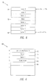
- Fig. 5 shows an example of a block structure 80 including a start-of-file location 84 and an end-of-file location 86 and a defective sector location 82, the latter of which is skipped over when writing to sectors 0 - 6.
- the information that was to be written to the defective sector is instead written to a location in a spare area in the system area.
- a defective sector/block can point to a spare location where it is replaced by the spare location. This requires that the defective sector/block have enough usable bytes where the location of the redirected sector can be saved.
- the controller should employ a unique method to guarantee the value saved in the spare location. This method can be programming the address in the defective sector in multiple locations and when accessed, the locations will be compared to validate the correct address.
- FIG. 6 An example 100 of another embodiment of the present invention will be explained with reference to Fig. 6.
- some of the data stored within certain locations of the one-time programmable nonvolatile memory may be corrupted.
- the system needs to recognize the occurrence of a power failure so that a file that includes corrupted data will be identified as an invalid file and following files will be stored at a valid location not adversely affected by power failures.
- the system verifies the error correction code (ECC) associated with the particular sector, if the ECC indicates that the particular sector or any portions thereof is corrupt, the next sector is read.
- ECC error correction code
- the system continues to check for an end-of-file identifier to determine whether or not the file has been properly written and that the ECC error is due to grown error(s) rather than power failure related errors. If there is no start-of-file identifier at a location following the corrupt sector or there is no end-of-file in the rest of the media, such location can be identified as a corrupt sector due to power failure and designated accordingly so as to prevent future storage of information therein.
- the next sector is read and if all of the data in the next sector is in a non-programmable state, i.e. all 0's or all 1's, and/or the ECC associated with the next sector indicates error, then it is determined that the end-of-file has been reached.
- the sector following the next sector is read and the same criteria is implemented, i.e. a determination is made as to whether all of the data in the sector is in a non-programmable state and/or the sector-associated ECC indicates an error and based upon the outcome, a determination is made as to whether or not the end-of-file is reached.
- the system when there are more than one power failures in a media, there may be more than one corrupted sector and thus the system must verify all locations and where new file locations are started and ended. In other words, the system can maintain a table of corrupted files in a spare area so that after power-up, the system can identify and map the corrupted files thereby preventing their use for future storage.
- the start-of-file is designated at sector 0 at 102 and remaining sectors of the file are stored in following sector locations, such as sector 1 104 and sector 2 106.
- sector 3 108 has been adversely affected or corrupted by a power failure, thus, a new file will be stored starting from 110.
- the embodiments of the invention relate to one time programmable non-volatile memories used for data such as camera images to allow data to be updated even though the memory medium cannot be overwritten.
- the embodiments provide one-time programmable memory for writing files in applications requiring re-writing of sector information, such as digital cameras, on a partial programmable basis, i.e. bit-by-bit, byte-by-byte or word-by-word basis, while maintaining backward compatibility with DOS-like or other known file systems.
- the above is achieved by comparing a sector that is being re-written by the host to the same sector that was previously written by the host and by identifying, on a bit-by-bit, byte-by-byte or word-by-word basis, which bits, bytes or words of the previously written sector have been modified since, typically, not all of the bits of a sector are modified each time it is re-written by the host. Once this identification has been made, one of the three methods can be performed.
- One method is to determine if the bits, bytes or words being modified, or identified to be modified, have even been programmed the first time around in the one-time programmable memory.
- a binary state of '1' in non-volatile memory, while meaning '1' or a high state, is nevertheless a non-programmed state because after initial manufacturing of the memory, all bits are programmed to '1'.
- the modified information is written to a spare area in a location that is within the same sector that is being re-written and in yet a third method, the modified information is written to a spare location outside of the sector being re-written, such as the spare locations discussed in the specification.
- a pointer is used to point to the spare area that now contains the modified bits, bytes or words for future reading of the re-written sector.
- This pointer is kept in the overhead portion of the sector in the one-time programmable memory.
- the pointer maintains track of the bits, bytes or words that are changed but it does so for the sector that it is presently a part thereof.
- sector X is stored along with its overhead in a particular location in the one-time programmable memory and if it is re-written by the host, the new version of the sector, along with its overhead, is written to a different area within the one-time memory with the pointer in the different area being a part of the overhead but reflecting the changed bits, bytes or words.
- the same area or location within the one-time memory is not occupied by the pointer reflecting a re-write of the sector, rather, a different location within the one-time memory is used to store the pointer reflecting the re-write.
- An alternative method is to simply write the modified bit, byte or words in the spare area altogether and to use a pointer to point to the spare location for future reading of the re-written sector.
- controller device 54 The operation of the controller device 54 is under the control of micro-processor 74 which operates in accordance with instructions defined by a computer program.
- An aspect of the present invention thus provides a storage medium storing processor implementable instructions for controlling a processor to carry out the method as hereinabove described.
- the computer program can be obtained in electronic form for example by downloading the code over a network such as the internet.
- an electrical signal carrying processor implementable instructions for controlling a processor to carry out the method as hereinbefore described.
Landscapes
- Engineering & Computer Science (AREA)
- Theoretical Computer Science (AREA)
- Human Computer Interaction (AREA)
- Physics & Mathematics (AREA)
- General Engineering & Computer Science (AREA)
- General Physics & Mathematics (AREA)
- Information Retrieval, Db Structures And Fs Structures Therefor (AREA)
- Techniques For Improving Reliability Of Storages (AREA)
- Signal Processing For Digital Recording And Reproducing (AREA)
- Read Only Memory (AREA)
Abstract
Description
Claims (28)
- A digital equipment system comprising:one-time-programmable nonvolatile memory for storing information organized into sectors based on commands received from the host and upon receiving commands from the host to re-write a sector, the controller device being operable for re-writing said sector on a bit-by-bit, byte-by-byte or word-for-word basis.a. a host for sending commands to read or write files having sectors of information, each sector being modifiable on a bit-by-bit, byte-by-byte or word-by-word basis, said host being operative to receive responses to said commands;b. a controller device responsive to said commands, and including,
- A digital equipment system as recited in claim 1 wherein said one-time-programmable nonvolatile memory includes a system area and a data area, said system area storing information pertaining to the organization of the information stored or to be stored in the data area.
- A digital equipment system as recited in claim 2 wherein said system area includes storage areas for including Original Engineering Manufacturer (OEM) identification/Bidirectional Input/Output System (BIOS), a File Allocation Table (FAT) 1, a FAT 2 and root disk directory information.
- A digital equipment system as recited in claim 1 wherein said controller device further includes a first buffer for storing a host-provided sector and a second buffer for storing sectors stored or to be stored in the one-time-programmable nonvolatile memory.
- A digital equipment system as recited in claim 4 further including a comparator coupled between said first and second buffer for comparing a sector to be modified or accessed by the host with those sectors to which information has been previously written.
- A digital equipment system as recited in claim 1 wherein during power-up, said controller device is operable for identifying the end-of-file, wherein the location following the location in which the end-of-file resides is identified as the location for the start-of-file of a new file to be stored.
- A digital equipment system as recited in claim 6 wherein said end-of-file is identified by the use of a flag.
- A digital equipment system as recited in claim 1 wherein said files are digital photographs.
- A digital equipment system as recited in claim 1 wherein said files are archives.
- A digital equipment system as recited in claim 1 wherein said controller device maintains a correlation between logical addresses and physical addresses for translating host-provided addresses to addresses recognized by the one-time-programmable nonvolatile memory.
- A digital equipment system as recited in claim 10 wherein said controller is operable for maintaining track of defective locations within the one-time-programmable nonvolatile memory.
- A digital equipment system comprising:one-time-programmable nonvolatile memory for storing information organized into sectors, based on commands received from the host, and upon commands from the host to re-write a sector, said one-time-programmable nonvolatile memory including a spare area, said controller being operable for mapping sectors being re-written to spare area.a. a host for sending commands to read or write files having sectors of information, said host being operative to receive responses to said commands;b. a controller device responsive to said commands, and including,
- A digital equipment system as recited in claim 12 wherein said one-time-programmable nonvolatile memory further includes a system area and a data area.
- A digital equipment system as recited in claim 13 wherein said controller device is operable for identifying a start-of-file location and an end-of-file location and a defective sector location within the one-time-programmable nonvolatile memory, the latter of which is skipped over when writing sectors.
- A digital equipment system as recited in claim 14 wherein the information that was to be written to the defective sector is instead written to the spare area location.
- A digital equipment system as recited in claim 12 wherein said controller is operable for determining if there is no start-of-file identifier at a location following a corrupted sector or there is no end-of-file in the rest of the one-time-programmable nonvolatile memory, such location identified as a corrupted sector due to power failure and designated accordingly so as to prevent future storage of information therein.
- A digital equipment system comprising:one-time-programmable nonvolatile memory for storing files and identifying the start-of-file and end-of-file for a file being stored within the one-time-programmable memory, wherein during power-up, said controller device for identifying the end-of-file of a stored file, the location following the location in which the end-of-file resides being identified as the location for the start-of-file of a new file to be stored.a. a host for sending commands to read or write files, said host being operative to receive responses to said commands;b. a controller device responsive to said commands, and including,
- A digital equipment system comprising:a. a host for sending commands to read or write files having sectors of information, said host being operative to receive responses to said commands;b. a controller device responsive to said commands, and including,
one-time-programmable nonvolatile memory having spare locations for storing sector information, said one-time-programmable nonvolatile memory for storing information organized into sectors based on commands received from the host and upon receiving a command from the host to re-write or update a sector, the controller device for writing the updated sector to a spare location. - A digital equipment system comprising:one-time-programmable nonvolatile memory for storing information organized into sectors, wherein said controller checks the ECC of a particular sector for a determination of whether or not the particular sector is corrupted and if so, reads the information stored within the next sector and determines if the next sector information is in a non-programmable state and if so or the ECC associated with the next sector indicates that the next sector information is corrupt, the controller device identifies an end-of-file.a. a host for sending commands to read or write files having sectors of information, each sector having associated therewith an error correction code (ECC) indicative of the corruption of sector information, said host being operative to receive responses to said commands;b. a controller device responsive to said commands, and including,
- A digital equipment system comprising:a. a host for sending commands to read or write files in portions corresponding to memory sectors, each sector being identifiable on a bit-by-bit, byte-by-byte or word-by-word basis, said host being operable for commanding to re-write a previously written sector; andb. a controller device responsive to the host commands and including, one-time-programmable non-volatile memory for storing information organized into sectors based on commands received from the host, said memory having stored therein the previously written sector and upon receiving a command from the host to re-write the previously written sector, the controller device being operable for performing partial programming of the previously written sector to write the sector to be re-written on a bit-by-bit, byte-by-byte or word-by-word basis.
- A digital equipment system, as recited in claim 20, wherein the controller device is operable for comparing the sector to be re-written to the previously written sector and for identifying which bits, bytes or words of the sector to be re-written are modified and, if said identified bits, bytes or words were not previously programmed in the previously written sector, programming the same.
- A digital equipment system, as recited in claim 20, wherein said memory includes spare locations and further wherein the controller device is operable for comparing the sector to be re-written to the previously written sector and for identifying which bits, bytes or words of the sector to be re-written are modified and writing said identified bits, bytes or words in said spare locations.
- A method of re-writing sectors to previously written sectors within a one-time-programmable memory comprising:a. receiving a command to re-write a previously written sector to a one-time-programmable memory, said previously written sector having bits, bytes or words;b. comparing a sector to be re-written to said previously written sector for modifications to the latter, said sector to be re-written having bits, bytes or words;c. identifying bits, bytes or words of the previously written sector that are modified;d. determining if the modified bits, bytes or words of the previously written sector have not programmed; ande. programming the determined modified bits, bytes or words of the previously written sector to make the previously written sector include the same information as the sector to be re-written.
- A method of re-writing sectors to previously written sectors within a one-time-programmable memory comprising:a. receiving a command to re-write a previously written sector to a one-time-programmable memory, said previously written sector having bits, bytes or words;b. comparing a sector to be re-written to said previously written sector for modifications to the latter, said sector to be re-written having bits, bytes or words;c. identifying bits, bytes or words of the previously written sector that are modified;d. determining if the modified bits, bytes or words of the previously written sector have not programmed; ande. writing the modified bits, bytes or words into a spare location within the one-time-programmable memory.
- A memory system comprising:an interface for receiving commands from a host for the writing of data to and reading of data from the memory system;a one-time programmable memory having a data area divided into physical sectors;a control device responsive to the commands and comprising means for emulating a re-programmable memory whereby logical addresses available to the host are presented to the host as being mapped to re-writable virtual sectors in the emulated memory and are actually mapped to physical addresses in the physical sectors in the one-time-programmable memory;the control device comprising a comparator responsive to a command to rewrite a virtual sector with new data by comparing the new data with contents of a physical sector in which existing data for the virtual sector was previously programmed to identify portions of said new data which are different from the existing data; andpartial programming means for programming only the identified portions of the new data into previously unprogrammed areas of the memory and for maintaining mapping of the logical addresses for the re-written virtual sector to locations in the memory containing the new data.
- A method of operating a memory system comprising a one-time programmable memory having a data area divided into physical sectors;:the method comprising:receiving commands from a host for the writing of data to and reading of data from the memory system;operating a control device responsive to the commands to emulate a re-programmable memory whereby logical addresses available to the host are presented to the host as being mapped to re-writable virtual sectors in the emulated memory and are actually mapped to physical addresses in the physical sectors in the one-time-programmable memory;the control device being responsive to a command to rewrite a virtual sector with new data by comparing the new data with contents of a physical sector in which existing data for the virtual sector was previously programmed to identify portions of said new data which are different from the existing data; andpartial programming the memory by programming only the identified portions of the new data into previously unprogrammed areas of the memory and maintaining mapping of the logical addresses for the re-written virtual sector to locations in the memory containing the new data.
- A storage medium storing processor implementable instructions for controlling a processor to carry out the method of any one of claims 23, 24, and 26.
- An electrical signal carrying processor implementable instructions for controlling a processor to carry out the method of any one of claims 23, 24 and 26.
Applications Claiming Priority (2)
| Application Number | Priority Date | Filing Date | Title |
|---|---|---|---|
| US54451 | 1987-05-26 | ||
| US10/054,451 US6957295B1 (en) | 2002-01-18 | 2002-01-18 | File management of one-time-programmable nonvolatile memory devices |
Publications (2)
| Publication Number | Publication Date |
|---|---|
| EP1331548A2 true EP1331548A2 (en) | 2003-07-30 |
| EP1331548A3 EP1331548A3 (en) | 2006-05-10 |
Family
ID=21991148
Family Applications (1)
| Application Number | Title | Priority Date | Filing Date |
|---|---|---|---|
| EP03250314A Withdrawn EP1331548A3 (en) | 2002-01-18 | 2003-01-17 | File management of one-time-programmable non volatile memory devices |
Country Status (3)
| Country | Link |
|---|---|
| US (1) | US6957295B1 (en) |
| EP (1) | EP1331548A3 (en) |
| JP (1) | JP4268396B2 (en) |
Cited By (9)
| Publication number | Priority date | Publication date | Assignee | Title |
|---|---|---|---|---|
| US6895490B1 (en) | 2001-04-09 | 2005-05-17 | Matrix Semiconductor, Inc. | Method for making a write-once memory device read compatible with a write-many file system |
| US6996660B1 (en) | 2001-04-09 | 2006-02-07 | Matrix Semiconductor, Inc. | Memory device and method for storing and reading data in a write-once memory array |
| US7003619B1 (en) | 2001-04-09 | 2006-02-21 | Matrix Semiconductor, Inc. | Memory device and method for storing and reading a file system structure in a write-once memory array |
| WO2006023196A2 (en) | 2004-08-24 | 2006-03-02 | Sandisk 3D Llc | Method and apparatus for using a one-time or few-time programmable memory with a host device designed for erasable/rewriteable memory |
| US7051251B2 (en) | 2002-12-20 | 2006-05-23 | Matrix Semiconductor, Inc. | Method for storing data in a write-once memory array using a write-many file system |
| US7062602B1 (en) | 2001-04-09 | 2006-06-13 | Matrix Semiconductor, Inc. | Method for reading data in a write-once memory device using a write-many file system |
| WO2013048485A1 (en) * | 2011-09-30 | 2013-04-04 | Intel Corporation | Autonomous initialization of non-volatile random access memory in a computer system |
| US9430372B2 (en) | 2011-09-30 | 2016-08-30 | Intel Corporation | Apparatus, method and system that stores bios in non-volatile random access memory |
| US9529708B2 (en) | 2011-09-30 | 2016-12-27 | Intel Corporation | Apparatus for configuring partitions within phase change memory of tablet computer with integrated memory controller emulating mass storage to storage driver based on request from software |
Families Citing this family (25)
| Publication number | Priority date | Publication date | Assignee | Title |
|---|---|---|---|---|
| US6728851B1 (en) * | 1995-07-31 | 2004-04-27 | Lexar Media, Inc. | Increasing the memory performance of flash memory devices by writing sectors simultaneously to multiple flash memory devices |
| US8171203B2 (en) | 1995-07-31 | 2012-05-01 | Micron Technology, Inc. | Faster write operations to nonvolatile memory using FSInfo sector manipulation |
| US5845313A (en) | 1995-07-31 | 1998-12-01 | Lexar | Direct logical block addressing flash memory mass storage architecture |
| US6978342B1 (en) | 1995-07-31 | 2005-12-20 | Lexar Media, Inc. | Moving sectors within a block of information in a flash memory mass storage architecture |
| US7102671B1 (en) | 2000-02-08 | 2006-09-05 | Lexar Media, Inc. | Enhanced compact flash memory card |
| US7167944B1 (en) | 2000-07-21 | 2007-01-23 | Lexar Media, Inc. | Block management for mass storage |
| GB0123417D0 (en) | 2001-09-28 | 2001-11-21 | Memquest Ltd | Improved data processing |
| GB0123416D0 (en) | 2001-09-28 | 2001-11-21 | Memquest Ltd | Non-volatile memory control |
| GB0123421D0 (en) | 2001-09-28 | 2001-11-21 | Memquest Ltd | Power management system |
| GB0123415D0 (en) | 2001-09-28 | 2001-11-21 | Memquest Ltd | Method of writing data to non-volatile memory |
| GB0123410D0 (en) | 2001-09-28 | 2001-11-21 | Memquest Ltd | Memory system for data storage and retrieval |
| US7231643B1 (en) | 2002-02-22 | 2007-06-12 | Lexar Media, Inc. | Image rescue system including direct communication between an application program and a device driver |
| WO2004063911A1 (en) * | 2003-01-16 | 2004-07-29 | Koninklijke Philips Electronics N.V. | Preventing distribution of modified or corrupted files |
| EP1695304A4 (en) | 2003-12-17 | 2011-09-28 | Lexar Media Inc | Electronic equipment point-of-sale activation to avoid theft |
| US7725628B1 (en) | 2004-04-20 | 2010-05-25 | Lexar Media, Inc. | Direct secondary device interface by a host |
| US7370166B1 (en) | 2004-04-30 | 2008-05-06 | Lexar Media, Inc. | Secure portable storage device |
| US7594063B1 (en) | 2004-08-27 | 2009-09-22 | Lexar Media, Inc. | Storage capacity status |
| US7464306B1 (en) | 2004-08-27 | 2008-12-09 | Lexar Media, Inc. | Status of overall health of nonvolatile memory |
| US7509526B2 (en) * | 2004-09-24 | 2009-03-24 | Seiko Epson Corporation | Method of correcting NAND memory blocks and to a printing device employing the method |
| US8429375B1 (en) * | 2006-06-16 | 2013-04-23 | Synopsys, Inc. | Memory management unit (MMU) to make only one time programmable (OTP) memory appear multiple times programmable (MTP) |
| US7650458B2 (en) * | 2006-06-23 | 2010-01-19 | Microsoft Corporation | Flash memory driver |
| US7783956B2 (en) * | 2006-07-12 | 2010-08-24 | Cronera Systems Incorporated | Data recorder |
| US20080027892A1 (en) * | 2006-07-27 | 2008-01-31 | Kestrelink Corporation | Dynamic stream file system network support |
| US8122322B2 (en) | 2007-07-31 | 2012-02-21 | Seagate Technology Llc | System and method of storing reliability data |
| US11099949B2 (en) * | 2018-08-03 | 2021-08-24 | Cirrus Logic, Inc. | Method apparatus for resuming and recovery checking from interrupted programming of one-time programmable memory device |
Family Cites Families (245)
| Publication number | Priority date | Publication date | Assignee | Title |
|---|---|---|---|---|
| JPS52130536A (en) | 1976-04-26 | 1977-11-01 | Toshiba Corp | Semiconductor memory unit |
| US4099069A (en) | 1976-10-08 | 1978-07-04 | Westinghouse Electric Corp. | Circuit producing a common clear signal for erasing selected arrays in a mnos memory system |
| US4398248A (en) | 1980-10-20 | 1983-08-09 | Mcdonnell Douglas Corporation | Adaptive WSI/MNOS solid state memory system |
| GB2020437B (en) | 1978-04-14 | 1982-08-04 | Seiko Instr & Electronics | Voltage detecting circuit |
| US4210959A (en) | 1978-05-10 | 1980-07-01 | Apple Computer, Inc. | Controller for magnetic disc, recorder, or the like |
| FR2426938A1 (en) | 1978-05-26 | 1979-12-21 | Cii Honeywell Bull | DEVICE FOR DETECTION OF DEFECTIVE SECTORS AND ALLOCATION OF REPLACEMENT SECTORS IN A DISK MEMORY |
| JPS559260A (en) | 1978-07-03 | 1980-01-23 | Nec Corp | Information processing system |
| US4532590A (en) | 1980-04-25 | 1985-07-30 | Data General Corporation | Data processing system having a unique address translation unit |
| US4355376A (en) | 1980-09-30 | 1982-10-19 | Burroughs Corporation | Apparatus and method for utilizing partially defective memory devices |
| JPS5764383A (en) | 1980-10-03 | 1982-04-19 | Toshiba Corp | Address converting method and its device |
| JPS57132256A (en) | 1981-02-09 | 1982-08-16 | Sony Corp | Memory device |
| JPS5877034A (en) | 1981-10-30 | 1983-05-10 | Hitachi Ltd | Recording method |
| US4473878A (en) | 1981-11-23 | 1984-09-25 | Motorola, Inc. | Memory management unit |
| US4476526A (en) | 1981-11-27 | 1984-10-09 | Storage Technology Corporation | Cache buffered memory subsystem |
| US4468730A (en) | 1981-11-27 | 1984-08-28 | Storage Technology Corporation | Detection of sequential data stream for improvements in cache data storage |
| US4450559A (en) | 1981-12-24 | 1984-05-22 | International Business Machines Corporation | Memory system with selective assignment of spare locations |
| JPS58215795A (en) | 1982-06-08 | 1983-12-15 | Toshiba Corp | Non-volatile memory device |
| JPS58215794A (en) | 1982-06-08 | 1983-12-15 | Toshiba Corp | Non-volatile memory device |
| US4498146A (en) | 1982-07-30 | 1985-02-05 | At&T Bell Laboratories | Management of defects in storage media |
| JPS5945695A (en) | 1982-09-07 | 1984-03-14 | Fujitsu Ltd | Ic memory |
| US4710871A (en) | 1982-11-01 | 1987-12-01 | Ncr Corporation | Data transmitting and receiving apparatus |
| JPS5992485U (en) | 1982-12-13 | 1984-06-22 | 日本ビクター株式会社 | tape cassette |
| JPS59162695A (en) | 1983-03-07 | 1984-09-13 | Nec Corp | Storage device |
| US4609833A (en) | 1983-08-12 | 1986-09-02 | Thomson Components-Mostek Corporation | Simple NMOS voltage reference circuit |
| JPS6074020A (en) * | 1983-09-30 | 1985-04-26 | Toshiba Corp | Storage device |
| US4896262A (en) | 1984-02-24 | 1990-01-23 | Kabushiki Kaisha Meidensha | Emulation device for converting magnetic disc memory mode signal from computer into semiconductor memory access mode signal for semiconductor memory |
| JPS60212900A (en) | 1984-04-09 | 1985-10-25 | Nec Corp | Semiconductor fixed memory |
| JPH0618018B2 (en) | 1984-05-22 | 1994-03-09 | キヤノン株式会社 | Portable information processing device |
| JPS618798A (en) | 1984-06-21 | 1986-01-16 | Nec Corp | Nonvolatile storage device |
| JPS6180597A (en) | 1984-09-26 | 1986-04-24 | Hitachi Ltd | semiconductor storage device |
| JPS6196598A (en) | 1984-10-17 | 1986-05-15 | Fuji Electric Co Ltd | Count data memory method of electric erasable p-rom |
| US4654847A (en) | 1984-12-28 | 1987-03-31 | International Business Machines | Apparatus for automatically correcting erroneous data and for storing the corrected data in a common pool alternate memory array |
| JPS61208673A (en) | 1985-03-12 | 1986-09-17 | Matsushita Electric Ind Co Ltd | Information recording and reproducing device |
| US4744062A (en) | 1985-04-23 | 1988-05-10 | Hitachi, Ltd. | Semiconductor integrated circuit with nonvolatile memory |
| US4829169A (en) | 1985-07-01 | 1989-05-09 | Toppan Moore Company, Inc. | IC card having state marker for record access |
| JPH0635227B2 (en) | 1985-07-31 | 1994-05-11 | トツパン・ム−ア株式会社 | IC card having means for reading update information and history information |
| JPS62102482A (en) | 1985-10-28 | 1987-05-12 | Matsushita Electric Ind Co Ltd | Information recording and reproducing device |
| US4800520A (en) | 1985-10-29 | 1989-01-24 | Kabushiki Kaisha Toshiba | Portable electronic device with garbage collection function |
| JP2664137B2 (en) | 1985-10-29 | 1997-10-15 | 凸版印刷株式会社 | IC card |
| US4746998A (en) | 1985-11-20 | 1988-05-24 | Seagate Technology, Inc. | Method for mapping around defective sectors in a disc drive |
| US4924331A (en) | 1985-11-20 | 1990-05-08 | Seagate Technology, Inc. | Method for mapping around defective sectors in a disc drive |
| DE3640238A1 (en) | 1985-11-30 | 1987-06-25 | Toshiba Kawasaki Kk | PORTABLE ELECTRONIC DEVICE |
| US4757474A (en) | 1986-01-28 | 1988-07-12 | Fujitsu Limited | Semiconductor memory device having redundancy circuit portion |
| JPH07114499B2 (en) | 1986-12-24 | 1995-12-06 | 株式会社日立製作所 | Data encoding method |
| JPS62283495A (en) | 1986-05-30 | 1987-12-09 | Ricoh Co Ltd | Read only memory |
| JPH07109717B2 (en) | 1986-05-31 | 1995-11-22 | キヤノン株式会社 | Memory write control method |
| JPH0784871B2 (en) | 1986-06-12 | 1995-09-13 | 株式会社日立製作所 | Vacuum exhaust device |
| SU1388877A1 (en) | 1986-09-16 | 1988-04-15 | Таганрогский радиотехнический институт им.В.Д.Калмыкова | Device for addressing storage units |
| SU1408439A1 (en) | 1986-10-20 | 1988-07-07 | Предприятие П/Я В-2129 | Addressing device for automatic configuration of computer memory |
| US4953122A (en) | 1986-10-31 | 1990-08-28 | Laserdrive Ltd. | Pseudo-erasable and rewritable write-once optical disk memory system |
| JPS63183700A (en) | 1987-01-26 | 1988-07-29 | Mitsubishi Electric Corp | Eeprom access method |
| JPH0636578Y2 (en) | 1987-04-10 | 1994-09-21 | 日本電気株式会社 | Semiconductor integrated circuit |
| JPS63198567U (en) | 1987-06-12 | 1988-12-21 | ||
| JPS6473430A (en) | 1987-09-14 | 1989-03-17 | Hudson Soft Co Ltd | Memory access control device |
| JPH081760B2 (en) | 1987-11-17 | 1996-01-10 | 三菱電機株式会社 | Semiconductor memory device |
| JP2696864B2 (en) | 1987-11-25 | 1998-01-14 | 日本電気株式会社 | Memory device |
| JPH01137817A (en) | 1987-11-25 | 1989-05-30 | Toshiba Corp | Delay circuit |
| SU1515164A1 (en) | 1988-01-12 | 1989-10-15 | Предприятие П/Я Г-4493 | Device for addressing a memory |
| SU1541619A1 (en) | 1988-05-30 | 1990-02-07 | Предприятие П/Я Г-4173 | Device for shaping address |
| US5198380A (en) | 1988-06-08 | 1993-03-30 | Sundisk Corporation | Method of highly compact EPROM and flash EEPROM devices |
| US5268870A (en) | 1988-06-08 | 1993-12-07 | Eliyahou Harari | Flash EEPROM system and intelligent programming and erasing methods therefor |
| US5293560A (en) | 1988-06-08 | 1994-03-08 | Eliyahou Harari | Multi-state flash EEPROM system using incremental programing and erasing methods |
| US5268318A (en) | 1988-06-08 | 1993-12-07 | Eliyahou Harari | Highly compact EPROM and flash EEPROM devices |
| US5268319A (en) | 1988-06-08 | 1993-12-07 | Eliyahou Harari | Highly compact EPROM and flash EEPROM devices |
| US5168465A (en) | 1988-06-08 | 1992-12-01 | Eliyahou Harari | Highly compact EPROM and flash EEPROM devices |
| US4914529A (en) | 1988-07-18 | 1990-04-03 | Western Digital Corp. | Data disk defect handling using relocation ID fields |
| US5070474A (en) | 1988-07-26 | 1991-12-03 | Disk Emulation Systems, Inc. | Disk emulation system |
| JPH064399Y2 (en) | 1988-08-10 | 1994-02-02 | 株式会社セガ・エンタープライゼス | Sound generator |
| US5253351A (en) | 1988-08-11 | 1993-10-12 | Hitachi, Ltd. | Memory controller with a cache memory and control method of cache memory including steps of determining memory access threshold values |
| SU1573458A2 (en) | 1988-09-26 | 1990-06-23 | Войсковая Часть 32103 | Addressing device |
| JPH0793499B2 (en) | 1989-01-10 | 1995-10-09 | キヤノン株式会社 | Hole drilling method using laser |
| US5535328A (en) | 1989-04-13 | 1996-07-09 | Sandisk Corporation | Non-volatile memory system card with flash erasable sectors of EEprom cells including a mechanism for substituting defective cells |
| EP1031992B1 (en) | 1989-04-13 | 2006-06-21 | SanDisk Corporation | Flash EEPROM system |
| US5226168A (en) | 1989-04-25 | 1993-07-06 | Seiko Epson Corporation | Semiconductor memory configured to emulate floppy and hard disk magnetic storage based upon a determined storage capacity of the semiconductor memory |
| GB2231419B (en) * | 1989-05-05 | 1993-09-22 | Technophone Ltd | Updating prom information. |
| JPH02308738A (en) | 1989-05-22 | 1990-12-21 | Masao Shiotani | Fish reef for lobster |
| US5200959A (en) | 1989-10-17 | 1993-04-06 | Sundisk Corporation | Device and method for defect handling in semi-conductor memory |
| SU1686449A2 (en) | 1989-10-23 | 1991-10-23 | Войсковая Часть 32103 | Addressing device |
| US5247658A (en) | 1989-10-31 | 1993-09-21 | Microsoft Corporation | Method and system for traversing linked list record based upon write-once predetermined bit value of secondary pointers |
| JPH03228377A (en) | 1990-02-02 | 1991-10-09 | Toshiba Corp | Semiconductor device |
| US5218695A (en) | 1990-02-05 | 1993-06-08 | Epoch Systems, Inc. | File server system having high-speed write execution |
| US5220518A (en) | 1990-06-07 | 1993-06-15 | Vlsi Technology, Inc. | Integrated circuit memory with non-binary array configuration |
| US5303198A (en) | 1990-09-28 | 1994-04-12 | Fuji Photo Film Co., Ltd. | Method of recording data in memory card having EEPROM and memory card system using the same |
| EP0489204B1 (en) | 1990-12-04 | 1995-08-16 | Hewlett-Packard Limited | Reprogrammable data storage device |
| JPH04216392A (en) | 1990-12-18 | 1992-08-06 | Mitsubishi Electric Corp | Semiconductor storage device provided with block write function |
| GB2251324B (en) | 1990-12-31 | 1995-05-10 | Intel Corp | File structure for a non-volatile semiconductor memory |
| JPH04268284A (en) | 1991-02-22 | 1992-09-24 | Fuji Photo Film Co Ltd | Memory card |
| JP3126396B2 (en) | 1991-02-06 | 2001-01-22 | 株式会社東芝 | Nonvolatile semiconductor memory device |
| JPH04278297A (en) | 1991-03-07 | 1992-10-02 | Toshiba Corp | Nonvolatile semiconductor memory |
| US5270979A (en) | 1991-03-15 | 1993-12-14 | Sundisk Corporation | Method for optimum erasing of EEPROM |
| US5396468A (en) | 1991-03-15 | 1995-03-07 | Sundisk Corporation | Streamlined write operation for EEPROM system |
| US5504760A (en) | 1991-03-15 | 1996-04-02 | Sandisk Corporation | Mixed data encoding EEPROM system |
| US5663901A (en) | 1991-04-11 | 1997-09-02 | Sandisk Corporation | Computer memory cards using flash EEPROM integrated circuit chips and memory-controller systems |
| JPH04332999A (en) | 1991-05-07 | 1992-11-19 | Hitachi Koki Co Ltd | Method of using memory |
| JP2582487B2 (en) | 1991-07-12 | 1997-02-19 | インターナショナル・ビジネス・マシーンズ・コーポレイション | External storage system using semiconductor memory and control method thereof |
| US5430859A (en) | 1991-07-26 | 1995-07-04 | Sundisk Corporation | Solid state memory system including plural memory chips and a serialized bus |
| DE69223099T2 (en) | 1991-08-09 | 1998-06-10 | Toshiba Ave Kk | Recording device for a memory card |
| JP3229345B2 (en) | 1991-09-11 | 2001-11-19 | ローム株式会社 | Non-volatile IC memory |
| US6230233B1 (en) | 1991-09-13 | 2001-05-08 | Sandisk Corporation | Wear leveling techniques for flash EEPROM systems |
| US5438573A (en) | 1991-09-13 | 1995-08-01 | Sundisk Corporation | Flash EEPROM array data and header file structure |
| US5357462A (en) | 1991-09-24 | 1994-10-18 | Kabushiki Kaisha Toshiba | Electrically erasable and programmable non-volatile semiconductor memory with automatic write-verify controller |
| US5778418A (en) | 1991-09-27 | 1998-07-07 | Sandisk Corporation | Mass computer storage system having both solid state and rotating disk types of memory |
| US5227714A (en) | 1991-10-07 | 1993-07-13 | Brooktree Corporation | Voltage regulator |
| US5640528A (en) | 1991-10-24 | 1997-06-17 | Intel Corporation | Method and apparatus for translating addresses using mask and replacement value registers |
| US5315558A (en) | 1991-10-25 | 1994-05-24 | Vlsi Technology, Inc. | Integrated circuit memory with non-binary array configuration |
| US5359569A (en) | 1991-10-29 | 1994-10-25 | Hitachi Ltd. | Semiconductor memory |
| JPH05128877A (en) | 1991-11-07 | 1993-05-25 | Mitsubishi Electric Corp | Nonvolatile semiconductor memory device |
| JPH05151097A (en) | 1991-11-28 | 1993-06-18 | Fujitsu Ltd | Data management method for rewritable memory |
| JP3171901B2 (en) | 1992-02-05 | 2001-06-04 | セイコーインスツルメンツ株式会社 | Rewriting method of nonvolatile memory card |
| JPH05233426A (en) | 1992-02-20 | 1993-09-10 | Fujitsu Ltd | Flash memory using method |
| DE69326370T2 (en) | 1992-03-05 | 2000-01-20 | Kabushiki Kaisha Toshiba, Kawasaki | Non-volatile semiconductor memory device |
| FR2688333B1 (en) | 1992-03-06 | 1994-04-29 | Sgc Thomson Microelectronics S | DEVICE AND METHOD FOR DELETING BY SECTORS OF A FLASH EPROM MEMORY. |
| TW231343B (en) | 1992-03-17 | 1994-10-01 | Hitachi Seisakusyo Kk | |
| JP2830594B2 (en) | 1992-03-26 | 1998-12-02 | 日本電気株式会社 | Semiconductor memory device |
| JP3485938B2 (en) | 1992-03-31 | 2004-01-13 | 株式会社東芝 | Nonvolatile semiconductor memory device |
| US5267218A (en) | 1992-03-31 | 1993-11-30 | Intel Corporation | Nonvolatile memory card with a single power supply input |
| JP3323869B2 (en) | 1992-03-31 | 2002-09-09 | 株式会社東芝 | Nonvolatile semiconductor memory device |
| US5532962A (en) | 1992-05-20 | 1996-07-02 | Sandisk Corporation | Soft errors handling in EEPROM devices |
| US5381539A (en) | 1992-06-04 | 1995-01-10 | Emc Corporation | System and method for dynamically controlling cache management |
| DE4219145C1 (en) | 1992-06-11 | 1994-03-17 | Emitec Emissionstechnologie | Method and device for soldering a metallic honeycomb body |
| JP3328321B2 (en) | 1992-06-22 | 2002-09-24 | 株式会社日立製作所 | Semiconductor storage device |
| JPH0612863A (en) | 1992-06-26 | 1994-01-21 | Toshiba Corp | Dual port DRAM |
| US5592415A (en) | 1992-07-06 | 1997-01-07 | Hitachi, Ltd. | Non-volatile semiconductor memory |
| US5315541A (en) | 1992-07-24 | 1994-05-24 | Sundisk Corporation | Segmented column memory array |
| JP2768618B2 (en) | 1992-08-28 | 1998-06-25 | シャープ株式会社 | Semiconductor disk device |
| JPH06103748A (en) | 1992-09-16 | 1994-04-15 | Mitsubishi Electric Corp | Power control circuit for IC memory card |
| US5428621A (en) | 1992-09-21 | 1995-06-27 | Sundisk Corporation | Latent defect handling in EEPROM devices |
| JPH06131889A (en) | 1992-10-14 | 1994-05-13 | Toshiba Corp | Semiconductor filing device |
| JP3177015B2 (en) | 1992-10-14 | 2001-06-18 | 株式会社東芝 | Control method of semiconductor memory device |
| JPH06132747A (en) | 1992-10-20 | 1994-05-13 | Fujitsu Ltd | Semiconductor device |
| US5337275A (en) | 1992-10-30 | 1994-08-09 | Intel Corporation | Method for releasing space in flash EEPROM memory array to allow the storage of compressed data |
| US5357475A (en) | 1992-10-30 | 1994-10-18 | Intel Corporation | Method for detaching sectors in a flash EEPROM memory array |
| US5341330A (en) | 1992-10-30 | 1994-08-23 | Intel Corporation | Method for writing to a flash memory array during erase suspend intervals |
| US5341339A (en) | 1992-10-30 | 1994-08-23 | Intel Corporation | Method for wear leveling in a flash EEPROM memory |
| US5822781A (en) | 1992-10-30 | 1998-10-13 | Intel Corporation | Sector-based storage device emulator having variable-sized sector |
| US5734567A (en) | 1992-11-06 | 1998-03-31 | Siemens Aktiengesellschaft | Diagnosis system for a plant |
| JPH06149395A (en) | 1992-11-12 | 1994-05-27 | Nec Corp | Semiconductor device |
| US5581723A (en) | 1993-02-19 | 1996-12-03 | Intel Corporation | Method and apparatus for retaining flash block structure data during erase operations in a flash EEPROM memory array |
| JP2856621B2 (en) | 1993-02-24 | 1999-02-10 | インターナショナル・ビジネス・マシーンズ・コーポレイション | Batch erase nonvolatile memory and semiconductor disk device using the same |
| EP0613151A3 (en) | 1993-02-26 | 1995-03-22 | Tokyo Shibaura Electric Co | Semiconductor memory system including a flash EEPROM. |
| JP3594626B2 (en) | 1993-03-04 | 2004-12-02 | 株式会社ルネサステクノロジ | Non-volatile memory device |
| US5404485A (en) | 1993-03-08 | 1995-04-04 | M-Systems Flash Disk Pioneers Ltd. | Flash file system |
| JPH06266596A (en) | 1993-03-11 | 1994-09-22 | Hitachi Ltd | Flash memory file storage device and information processor |
| JP3477781B2 (en) | 1993-03-23 | 2003-12-10 | セイコーエプソン株式会社 | IC card |
| US5479638A (en) | 1993-03-26 | 1995-12-26 | Cirrus Logic, Inc. | Flash memory mass storage architecture incorporation wear leveling technique |
| US5485595A (en) | 1993-03-26 | 1996-01-16 | Cirrus Logic, Inc. | Flash memory mass storage architecture incorporating wear leveling technique without using cam cells |
| US5388083A (en) | 1993-03-26 | 1995-02-07 | Cirrus Logic, Inc. | Flash memory mass storage architecture |
| KR970008188B1 (en) | 1993-04-08 | 1997-05-21 | 가부시끼가이샤 히다찌세이사꾸쇼 | Flash memory control method and information processing device using the same |
| JP3330187B2 (en) | 1993-05-13 | 2002-09-30 | 株式会社リコー | Memory card |
| US5544355A (en) | 1993-06-14 | 1996-08-06 | Hewlett-Packard Company | Method and apparatus for query optimization in a relational database system having foreign functions |
| US5519847A (en) | 1993-06-30 | 1996-05-21 | Intel Corporation | Method of pipelining sequential writes in a flash memory |
| US5353256A (en) | 1993-06-30 | 1994-10-04 | Intel Corporation | Block specific status information in a memory device |
| US5329491A (en) | 1993-06-30 | 1994-07-12 | Intel Corporation | Nonvolatile memory card with automatic power supply configuration |
| US5422842A (en) | 1993-07-08 | 1995-06-06 | Sundisk Corporation | Method and circuit for simultaneously programming and verifying the programming of selected EEPROM cells |
| US5465338A (en) | 1993-08-24 | 1995-11-07 | Conner Peripherals, Inc. | Disk drive system interface architecture employing state machines |
| US5566314A (en) | 1993-08-30 | 1996-10-15 | Lucent Technologies Inc. | Flash memory device employing unused cell arrays to update files |
| JP2922116B2 (en) | 1993-09-02 | 1999-07-19 | 株式会社東芝 | Semiconductor storage device |
| JP3683915B2 (en) | 1993-09-24 | 2005-08-17 | 株式会社東芝 | Semiconductor memory device |
| JP3215237B2 (en) | 1993-10-01 | 2001-10-02 | 富士通株式会社 | Storage device and method for writing / erasing storage device |
| US5365127A (en) | 1993-10-18 | 1994-11-15 | Hewlett-Packard Company | Circuit for conversion from CMOS voltage levels to shifted ECL voltage levels with process compensation |
| US5430662A (en) | 1993-10-22 | 1995-07-04 | Sepa -- Group Ltd. | Laser projection system for truss manufacturing |
| JPH07141258A (en) | 1993-11-15 | 1995-06-02 | Toshiba Corp | Data recording / reproducing device |
| JPH07235193A (en) | 1993-12-28 | 1995-09-05 | Toshiba Corp | Semiconductor memory device |
| SG45399A1 (en) | 1994-01-12 | 1998-01-16 | Sun Microsystems Inc | Logically addressable physical memory for a virtual memory computer system that support multiple page sizes |
| US5473765A (en) | 1994-01-24 | 1995-12-05 | 3Com Corporation | Apparatus for using flash memory as a floppy disk emulator in a computer system |
| US6026027A (en) | 1994-01-31 | 2000-02-15 | Norand Corporation | Flash memory system having memory cache |
| US5661053A (en) | 1994-05-25 | 1997-08-26 | Sandisk Corporation | Method of making dense flash EEPROM cell array and peripheral supporting circuits formed in deposited field oxide with the use of spacers |
| US5603001A (en) | 1994-05-09 | 1997-02-11 | Kabushiki Kaisha Toshiba | Semiconductor disk system having a plurality of flash memories |
| JPH07311708A (en) | 1994-05-18 | 1995-11-28 | Fuji Film Micro Device Kk | Memory card |
| JP3092449B2 (en) | 1994-06-06 | 2000-09-25 | ヤマハ株式会社 | Semiconductor storage device |
| JPH0869696A (en) | 1994-08-31 | 1996-03-12 | Toshiba Corp | Semiconductor memory device |
| US5809558A (en) | 1994-09-29 | 1998-09-15 | Intel Corporation | Method and data storage system for storing data in blocks without file reallocation before erasure |
| US5508971A (en) | 1994-10-17 | 1996-04-16 | Sandisk Corporation | Programmable power generation circuit for flash EEPROM memory systems |
| JP2669365B2 (en) | 1994-11-24 | 1997-10-27 | 日本電気株式会社 | Rewritable ROM file device |
| US5537077A (en) | 1994-12-23 | 1996-07-16 | Advanced Micro Devices, Inc. | Power supply dependent method of controlling a charge pump |
| US5847552A (en) | 1995-01-24 | 1998-12-08 | Dell Usa, L.P. | Integrated circuit with determinate power source control |
| JPH08263361A (en) | 1995-03-23 | 1996-10-11 | Mitsubishi Electric Corp | Flash memory card |
| US5572465A (en) | 1995-05-25 | 1996-11-05 | Intel Corporation | Power supply configured sensing scheme for flash EEPROM |
| US6072796A (en) | 1995-06-14 | 2000-06-06 | Avid Technology, Inc. | Apparatus and method for accessing memory in a TDM network |
| US5723990A (en) | 1995-06-21 | 1998-03-03 | Micron Quantum Devices, Inc. | Integrated circuit having high voltage detection circuit |
| US5552698A (en) | 1995-06-29 | 1996-09-03 | United Microelectronics Corp. | Voltage supply system for IC chips |
| US5627416A (en) | 1995-07-21 | 1997-05-06 | Itt Corporation | Multi-voltage IC card host |
| US5930815A (en) | 1995-07-31 | 1999-07-27 | Lexar Media, Inc. | Moving sequential sectors within a block of information in a flash memory mass storage architecture |
| US5845313A (en) | 1995-07-31 | 1998-12-01 | Lexar | Direct logical block addressing flash memory mass storage architecture |
| US5907856A (en) | 1995-07-31 | 1999-05-25 | Lexar Media, Inc. | Moving sectors within a block of information in a flash memory mass storage architecture |
| US5838614A (en) | 1995-07-31 | 1998-11-17 | Lexar Microsystems, Inc. | Identification and verification of a sector within a block of mass storage flash memory |
| US6081878A (en) | 1997-03-31 | 2000-06-27 | Lexar Media, Inc. | Increasing the memory performance of flash memory devices by writing sectors simultaneously to multiple flash memory devices |
| JPH0969295A (en) | 1995-08-31 | 1997-03-11 | Sanyo Electric Co Ltd | Non-volatile multi-value memory device |
| US6125435A (en) | 1995-09-13 | 2000-09-26 | Lexar Media, Inc. | Alignment of cluster address to block addresses within a semiconductor non-volatile mass storage memory |
| US5835935A (en) | 1995-09-13 | 1998-11-10 | Lexar Media, Inc. | Method of and architecture for controlling system data with automatic wear leveling in a semiconductor non-volatile mass storage memory |
| US5809560A (en) | 1995-10-13 | 1998-09-15 | Compaq Computer Corporation | Adaptive read-ahead disk cache |
| KR100253868B1 (en) | 1995-11-13 | 2000-05-01 | 니시무로 타이죠 | Non-volatile semiconductor memory device |
| JP4299883B2 (en) | 1995-11-13 | 2009-07-22 | レクサー・メディア・インコーポレーテッド | Automatic voltage detection when multiple voltages are applied |
| JPH09147581A (en) | 1995-11-21 | 1997-06-06 | Hitachi Ltd | Semiconductor memory device and data processing device |
| US5799168A (en) | 1996-01-05 | 1998-08-25 | M-Systems Flash Disk Pioneers Ltd. | Standardized flash controller |
| JPH09212411A (en) | 1996-02-06 | 1997-08-15 | Tokyo Electron Ltd | Memory system |
| US5724303A (en) | 1996-02-15 | 1998-03-03 | Nexcom Technology, Inc. | Non-volatile programmable memory having an SRAM capability |
| US5787445A (en) | 1996-03-07 | 1998-07-28 | Norris Communications Corporation | Operating system including improved file management for use in devices utilizing flash memory as main memory |
| US5822252A (en) | 1996-03-29 | 1998-10-13 | Aplus Integrated Circuits, Inc. | Flash memory wordline decoder with overerase repair |
| US5991849A (en) | 1996-04-10 | 1999-11-23 | Sanyo Electric Co., Ltd | Rewriting protection of a size varying first region of a reprogrammable non-volatile memory |
| JP3493096B2 (en) | 1996-06-07 | 2004-02-03 | 株式会社東芝 | Semiconductor integrated circuit, IC card, and IC card system |
| US5959926A (en) | 1996-06-07 | 1999-09-28 | Dallas Semiconductor Corp. | Programmable power supply systems and methods providing a write protected memory having multiple interface capability |
| US5758100A (en) | 1996-07-01 | 1998-05-26 | Sun Microsystems, Inc. | Dual voltage module interconnect |
| US5757712A (en) | 1996-07-12 | 1998-05-26 | International Business Machines Corporation | Memory modules with voltage regulation and level translation |
| JP3761635B2 (en) | 1996-07-12 | 2006-03-29 | 株式会社ダックス | Memory board, memory access method, and memory access device |
| US5787484A (en) | 1996-08-08 | 1998-07-28 | Micron Technology, Inc. | System and method which compares data preread from memory cells to data to be written to the cells |
| US6021408A (en) | 1996-09-12 | 2000-02-01 | Veritas Software Corp. | Methods for operating a log device |
| US5920884A (en) | 1996-09-24 | 1999-07-06 | Hyundai Electronics America, Inc. | Nonvolatile memory interface protocol which selects a memory device, transmits an address, deselects the device, subsequently reselects the device and accesses data |
| US5860124A (en) | 1996-09-30 | 1999-01-12 | Intel Corporation | Method for performing a continuous over-write of a file in nonvolatile memory |
| US5754567A (en) | 1996-10-15 | 1998-05-19 | Micron Quantum Devices, Inc. | Write reduction in flash memory systems through ECC usage |
| US6047352A (en) | 1996-10-29 | 2000-04-04 | Micron Technology, Inc. | Memory system, method and predecoding circuit operable in different modes for selectively accessing multiple blocks of memory cells for simultaneous writing or erasure |
| US5890192A (en) | 1996-11-05 | 1999-03-30 | Sandisk Corporation | Concurrent write of multiple chunks of data into multiple subarrays of flash EEPROM |
| US5909586A (en) | 1996-11-06 | 1999-06-01 | The Foxboro Company | Methods and systems for interfacing with an interface powered I/O device |
| US5745418A (en) | 1996-11-25 | 1998-04-28 | Macronix International Co., Ltd. | Flash memory mass storage system |
| US5956473A (en) | 1996-11-25 | 1999-09-21 | Macronix International Co., Ltd. | Method and system for managing a flash memory mass storage system |
| JPH10154101A (en) | 1996-11-26 | 1998-06-09 | Toshiba Corp | Data storage system and cache control method applied to the system |
| JPH10177797A (en) | 1996-12-17 | 1998-06-30 | Toshiba Corp | Semiconductor storage device |
| JPH10187505A (en) | 1996-12-24 | 1998-07-21 | Toshiba Corp | Information storage system and data arrangement method applied to the system |
| US5901086A (en) | 1996-12-26 | 1999-05-04 | Motorola, Inc. | Pipelined fast-access floating gate memory architecture and method of operation |
| US6279069B1 (en) | 1996-12-26 | 2001-08-21 | Intel Corporation | Interface for flash EEPROM memory arrays |
| US5928370A (en) | 1997-02-05 | 1999-07-27 | Lexar Media, Inc. | Method and apparatus for verifying erasure of memory blocks within a non-volatile memory structure |
| US5822245A (en) | 1997-03-26 | 1998-10-13 | Atmel Corporation | Dual buffer flash memory architecture with multiple operating modes |
| US6122195A (en) | 1997-03-31 | 2000-09-19 | Lexar Media, Inc. | Method and apparatus for decreasing block write operation times performed on nonvolatile memory |
| US6034897A (en) | 1999-04-01 | 2000-03-07 | Lexar Media, Inc. | Space management for managing high capacity nonvolatile memory |
| US5953737A (en) | 1997-03-31 | 1999-09-14 | Lexar Media, Inc. | Method and apparatus for performing erase operations transparent to a solid state storage system |
| US6411546B1 (en) | 1997-03-31 | 2002-06-25 | Lexar Media, Inc. | Nonvolatile memory using flexible erasing methods and method and system for using same |
| US5831929A (en) | 1997-04-04 | 1998-11-03 | Micron Technology, Inc. | Memory device with staggered data paths |
| JP3592887B2 (en) | 1997-04-30 | 2004-11-24 | 株式会社東芝 | Nonvolatile semiconductor memory device |
| US6011322A (en) | 1997-07-28 | 2000-01-04 | Sony Corporation | Apparatus and method for providing power to circuitry implementing two different power sources |
| US6226708B1 (en) | 1997-08-18 | 2001-05-01 | Texas Instruments Incorporated | Method and system for efficiently programming non-volatile memory |
| US6011323A (en) | 1997-09-30 | 2000-01-04 | International Business Machines Corporation | Apparatus, method and article of manufacture providing for auxiliary battery conservation in adapters |
| US5937425A (en) | 1997-10-16 | 1999-08-10 | M-Systems Flash Disk Pioneers Ltd. | Flash file system optimized for page-mode flash technologies |
| JPH11224492A (en) | 1997-11-06 | 1999-08-17 | Toshiba Corp | Semiconductor storage device, nonvolatile semiconductor storage device, and flash memory |
| US5969986A (en) | 1998-06-23 | 1999-10-19 | Invox Technology | High-bandwidth read and write architectures for non-volatile memories |
| US6182162B1 (en) | 1998-03-02 | 2001-01-30 | Lexar Media, Inc. | Externally coupled compact flash memory card that configures itself one of a plurality of appropriate operating protocol modes of a host computer |
| US6040997A (en) | 1998-03-25 | 2000-03-21 | Lexar Media, Inc. | Flash memory leveling architecture having no external latch |
| US6055184A (en) | 1998-09-02 | 2000-04-25 | Texas Instruments Incorporated | Semiconductor memory device having programmable parallel erase operation |
| US6279114B1 (en) | 1998-11-04 | 2001-08-21 | Sandisk Corporation | Voltage negotiation in a single host multiple cards system |
| US6374337B1 (en) | 1998-11-17 | 2002-04-16 | Lexar Media, Inc. | Data pipelining method and apparatus for memory control circuit |
| JP3948692B2 (en) * | 1999-03-26 | 2007-07-25 | シャープ株式会社 | Semiconductor memory device |
| DE60030876T2 (en) | 1999-04-01 | 2007-05-03 | Lexar Media, Inc., Fremont | Scope management of a high-capacity non-volatile memory |
| US6141249A (en) | 1999-04-01 | 2000-10-31 | Lexar Media, Inc. | Organization of blocks within a nonvolatile memory unit to effectively decrease sector write operation time |
| US6181118B1 (en) | 1999-06-24 | 2001-01-30 | Analog Devices, Inc. | Control circuit for controlling a semi-conductor switch for selectively outputting an output voltage at two voltage levels |
| US6426893B1 (en) * | 2000-02-17 | 2002-07-30 | Sandisk Corporation | Flash eeprom system with simultaneous multiple data sector programming and storage of physical block characteristics in other designated blocks |
| TW539946B (en) | 2001-08-07 | 2003-07-01 | Solid State System Company Ltd | Window-based flash memory storage system, and the management method and the access method thereof |
-
2002
- 2002-01-18 US US10/054,451 patent/US6957295B1/en not_active Expired - Lifetime
- 2002-10-18 JP JP2002305005A patent/JP4268396B2/en not_active Expired - Lifetime
-
2003
- 2003-01-17 EP EP03250314A patent/EP1331548A3/en not_active Withdrawn
Cited By (19)
| Publication number | Priority date | Publication date | Assignee | Title |
|---|---|---|---|---|
| US7062602B1 (en) | 2001-04-09 | 2006-06-13 | Matrix Semiconductor, Inc. | Method for reading data in a write-once memory device using a write-many file system |
| US6996660B1 (en) | 2001-04-09 | 2006-02-07 | Matrix Semiconductor, Inc. | Memory device and method for storing and reading data in a write-once memory array |
| US7003619B1 (en) | 2001-04-09 | 2006-02-21 | Matrix Semiconductor, Inc. | Memory device and method for storing and reading a file system structure in a write-once memory array |
| US6895490B1 (en) | 2001-04-09 | 2005-05-17 | Matrix Semiconductor, Inc. | Method for making a write-once memory device read compatible with a write-many file system |
| US7051251B2 (en) | 2002-12-20 | 2006-05-23 | Matrix Semiconductor, Inc. | Method for storing data in a write-once memory array using a write-many file system |
| EP1782209A4 (en) * | 2004-08-24 | 2009-04-22 | Sandisk 3D Llc | METHOD AND APPARATUS FOR USING A PROGRAMMABLE MEMORY ONLY OR ONCE WITH A HOST DEVICE FOR ERASABLE / REINSCRIBIBLE MEMORY |
| US8209476B2 (en) | 2004-08-24 | 2012-06-26 | Sandisk 3D Llc | Method and apparatus for using a one-time or few-time programmable memory with a host device designed for erasable-rewriteable memory |
| US7398348B2 (en) | 2004-08-24 | 2008-07-08 | Sandisk 3D Llc | Method and apparatus for using a one-time or few-time programmable memory with a host device designed for erasable/rewritable memory |
| WO2006023196A2 (en) | 2004-08-24 | 2006-03-02 | Sandisk 3D Llc | Method and apparatus for using a one-time or few-time programmable memory with a host device designed for erasable/rewriteable memory |
| US7689805B2 (en) | 2004-08-24 | 2010-03-30 | Sandisk 3D Llc | Method and apparatus for using a one-time or few-time programmable memory with a host device designed for erasable/rewriteable memory |
| US7861058B2 (en) | 2004-08-24 | 2010-12-28 | Sandisk 3D Llc | Method and apparatus for using a one-time or few-time programmable memory with a host device designed for erasable/rewriteable memory |
| JP4852548B2 (en) * | 2004-08-24 | 2012-01-11 | サンディスク スリーディー エルエルシー. | Method and apparatus for using memory programmable once or several times in a host device designed for erasable / rewritable memory |
| JP2008511072A (en) * | 2004-08-24 | 2008-04-10 | サンディスク スリーディー エルエルシー. | Method and apparatus for using memory programmable once or several times in a host device designed for erasable / rewritable memory |
| WO2013048485A1 (en) * | 2011-09-30 | 2013-04-04 | Intel Corporation | Autonomous initialization of non-volatile random access memory in a computer system |
| US9378133B2 (en) | 2011-09-30 | 2016-06-28 | Intel Corporation | Autonomous initialization of non-volatile random access memory in a computer system |
| US9430372B2 (en) | 2011-09-30 | 2016-08-30 | Intel Corporation | Apparatus, method and system that stores bios in non-volatile random access memory |
| US9529708B2 (en) | 2011-09-30 | 2016-12-27 | Intel Corporation | Apparatus for configuring partitions within phase change memory of tablet computer with integrated memory controller emulating mass storage to storage driver based on request from software |
| US10001953B2 (en) | 2011-09-30 | 2018-06-19 | Intel Corporation | System for configuring partitions within non-volatile random access memory (NVRAM) as a replacement for traditional mass storage |
| US10055353B2 (en) | 2011-09-30 | 2018-08-21 | Intel Corporation | Apparatus, method and system that stores bios in non-volatile random access memory |
Also Published As
| Publication number | Publication date |
|---|---|
| JP4268396B2 (en) | 2009-05-27 |
| JP2003257132A (en) | 2003-09-12 |
| US6957295B1 (en) | 2005-10-18 |
| EP1331548A3 (en) | 2006-05-10 |
Similar Documents
| Publication | Publication Date | Title |
|---|---|---|
| US6957295B1 (en) | File management of one-time-programmable nonvolatile memory devices | |
| US6950918B1 (en) | File management of one-time-programmable nonvolatile memory devices | |
| JP4037605B2 (en) | Nonvolatile memory unit controller, memory system having the controller, and nonvolatile memory unit control method | |
| KR101004876B1 (en) | Power Management Blocks for Use in Nonvolatile Memory Systems | |
| US6823417B2 (en) | Memory controller for memory card manages file allocation table | |
| US5832493A (en) | Flash file management system | |
| US7877569B2 (en) | Reduction of fragmentation in nonvolatile memory using alternate address mapping | |
| US7610434B2 (en) | File recording apparatus | |
| US5611067A (en) | Nonvolatile semiconductor memory device having means for selective transfer of memory block contents and for chaining together unused memory blocks | |
| JP4633802B2 (en) | Nonvolatile storage device, data read method, and management table creation method | |
| US6820185B2 (en) | Method for identifying memory cells storing replacement data on a memory device | |
| US8185705B2 (en) | Information recording medium, information recording medium accessing apparatus and accessing method | |
| EP1548599A2 (en) | Faster write operations to nonvolatile memory by manipulation of frequently accessed sectors | |
| US6839798B1 (en) | Flash memory capable of storing frequently rewritten data | |
| US20100169556A1 (en) | Nonvolatile storage device, information recording system, and information recording method | |
| US20120084494A1 (en) | Memory for accessing multiple sectors of information substantially concurrently | |
| JP2002508862A (en) | Moving sectors in blocks in flash memory | |
| KR20000048766A (en) | Method for performing a continuous over-write of a file in a nonvolatile memory | |
| JP2009199625A (en) | Memory card, and method for controlling memory card and method for controlling nonvolatile semiconductor memory | |
| CN102239477A (en) | Continuous address space in non-volatile-memories (nvm) using efficient management methods for array deficiencies | |
| JPH10124384A (en) | Control method for nonvolatile semiconductor memory | |
| JP2010267290A (en) | Method and apparatus for resolving physical blocks associated with a common logical block | |
| US20050278480A1 (en) | Method of writing data into flash memory | |
| EP1359500B1 (en) | File management of one-time-programmable nonvolatile memory devices | |
| JP3784844B2 (en) | Semiconductor memory device |
Legal Events
| Date | Code | Title | Description |
|---|---|---|---|
| PUAI | Public reference made under article 153(3) epc to a published international application that has entered the european phase |
Free format text: ORIGINAL CODE: 0009012 |
|
| AK | Designated contracting states |
Designated state(s): AT BE BG CH CY CZ DE DK EE ES FI FR GB GR HU IE IT LI LU MC NL PT SE SI SK TR |
|
| AX | Request for extension of the european patent |
Extension state: AL LT LV MK RO |
|
| PUAL | Search report despatched |
Free format text: ORIGINAL CODE: 0009013 |
|
| AK | Designated contracting states |
Kind code of ref document: A3 Designated state(s): AT BE BG CH CY CZ DE DK EE ES FI FR GB GR HU IE IT LI LU MC NL PT SE SI SK TR |
|
| AX | Request for extension of the european patent |
Extension state: AL LT LV MK RO |
|
| RIC1 | Information provided on ipc code assigned before grant |
Ipc: G06F 12/06 20060101ALI20060317BHEP Ipc: G06F 12/02 20060101ALI20060317BHEP Ipc: G06F 3/06 20060101AFI20030430BHEP |
|
| 17P | Request for examination filed |
Effective date: 20061102 |
|
| AKX | Designation fees paid |
Designated state(s): DE FR GB IT |
|
| 17Q | First examination report despatched |
Effective date: 20070112 |
|
| STAA | Information on the status of an ep patent application or granted ep patent |
Free format text: STATUS: THE APPLICATION HAS BEEN WITHDRAWN |
|
| 18W | Application withdrawn |
Effective date: 20131112 |