EP1293588B1 - Plasma cvd apparatus and method - Google Patents
Plasma cvd apparatus and method Download PDFInfo
- Publication number
- EP1293588B1 EP1293588B1 EP01932112A EP01932112A EP1293588B1 EP 1293588 B1 EP1293588 B1 EP 1293588B1 EP 01932112 A EP01932112 A EP 01932112A EP 01932112 A EP01932112 A EP 01932112A EP 1293588 B1 EP1293588 B1 EP 1293588B1
- Authority
- EP
- European Patent Office
- Prior art keywords
- electrode
- feeding
- plasma cvd
- frequency power
- high frequency
- Prior art date
- Legal status (The legal status is an assumption and is not a legal conclusion. Google has not performed a legal analysis and makes no representation as to the accuracy of the status listed.)
- Expired - Lifetime
Links
- 238000000034 method Methods 0.000 title abstract description 20
- 239000000758 substrate Substances 0.000 claims abstract description 63
- 238000005268 plasma chemical vapour deposition Methods 0.000 claims abstract description 56
- 239000010409 thin film Substances 0.000 claims abstract description 33
- 238000006243 chemical reaction Methods 0.000 claims abstract description 19
- 239000010408 film Substances 0.000 description 74
- 238000000151 deposition Methods 0.000 description 32
- 238000009826 distribution Methods 0.000 description 31
- 230000008021 deposition Effects 0.000 description 30
- 239000007789 gas Substances 0.000 description 13
- 229920006362 Teflon® Polymers 0.000 description 11
- 239000004809 Teflon Substances 0.000 description 10
- 230000003247 decreasing effect Effects 0.000 description 9
- 230000015572 biosynthetic process Effects 0.000 description 8
- 238000005755 formation reaction Methods 0.000 description 8
- 229910021417 amorphous silicon Inorganic materials 0.000 description 6
- 238000004140 cleaning Methods 0.000 description 6
- 230000005284 excitation Effects 0.000 description 6
- 238000010586 diagram Methods 0.000 description 4
- 229910001220 stainless steel Inorganic materials 0.000 description 4
- 239000010935 stainless steel Substances 0.000 description 4
- 230000007423 decrease Effects 0.000 description 3
- 230000000694 effects Effects 0.000 description 3
- 238000011835 investigation Methods 0.000 description 3
- 238000012423 maintenance Methods 0.000 description 3
- 239000000463 material Substances 0.000 description 3
- BLRPTPMANUNPDV-UHFFFAOYSA-N Silane Chemical compound [SiH4] BLRPTPMANUNPDV-UHFFFAOYSA-N 0.000 description 2
- 238000005452 bending Methods 0.000 description 2
- 238000000265 homogenisation Methods 0.000 description 2
- 230000003993 interaction Effects 0.000 description 2
- 230000002452 interceptive effect Effects 0.000 description 2
- 229910052782 aluminium Inorganic materials 0.000 description 1
- PNEYBMLMFCGWSK-UHFFFAOYSA-N aluminium oxide Inorganic materials [O-2].[O-2].[O-2].[Al+3].[Al+3] PNEYBMLMFCGWSK-UHFFFAOYSA-N 0.000 description 1
- 230000008859 change Effects 0.000 description 1
- 239000004020 conductor Substances 0.000 description 1
- 229910052802 copper Inorganic materials 0.000 description 1
- 239000003989 dielectric material Substances 0.000 description 1
- 238000002474 experimental method Methods 0.000 description 1
- 239000011521 glass Substances 0.000 description 1
- 229910010272 inorganic material Inorganic materials 0.000 description 1
- 239000011147 inorganic material Substances 0.000 description 1
- 239000012212 insulator Substances 0.000 description 1
- 230000007246 mechanism Effects 0.000 description 1
- 239000002184 metal Substances 0.000 description 1
- 229910052751 metal Inorganic materials 0.000 description 1
- 239000011368 organic material Substances 0.000 description 1
- 230000008569 process Effects 0.000 description 1
- 239000010453 quartz Substances 0.000 description 1
- 230000009467 reduction Effects 0.000 description 1
- VYPSYNLAJGMNEJ-UHFFFAOYSA-N silicon dioxide Inorganic materials O=[Si]=O VYPSYNLAJGMNEJ-UHFFFAOYSA-N 0.000 description 1
- 238000000427 thin-film deposition Methods 0.000 description 1
- 238000011282 treatment Methods 0.000 description 1
Images


Classifications
-
- H—ELECTRICITY
- H01—ELECTRIC ELEMENTS
- H01J—ELECTRIC DISCHARGE TUBES OR DISCHARGE LAMPS
- H01J37/00—Discharge tubes with provision for introducing objects or material to be exposed to the discharge, e.g. for the purpose of examination or processing thereof
- H01J37/32—Gas-filled discharge tubes
- H01J37/32009—Arrangements for generation of plasma specially adapted for examination or treatment of objects, e.g. plasma sources
- H01J37/32082—Radio frequency generated discharge
- H01J37/321—Radio frequency generated discharge the radio frequency energy being inductively coupled to the plasma
-
- C—CHEMISTRY; METALLURGY
- C23—COATING METALLIC MATERIAL; COATING MATERIAL WITH METALLIC MATERIAL; CHEMICAL SURFACE TREATMENT; DIFFUSION TREATMENT OF METALLIC MATERIAL; COATING BY VACUUM EVAPORATION, BY SPUTTERING, BY ION IMPLANTATION OR BY CHEMICAL VAPOUR DEPOSITION, IN GENERAL; INHIBITING CORROSION OF METALLIC MATERIAL OR INCRUSTATION IN GENERAL
- C23C—COATING METALLIC MATERIAL; COATING MATERIAL WITH METALLIC MATERIAL; SURFACE TREATMENT OF METALLIC MATERIAL BY DIFFUSION INTO THE SURFACE, BY CHEMICAL CONVERSION OR SUBSTITUTION; COATING BY VACUUM EVAPORATION, BY SPUTTERING, BY ION IMPLANTATION OR BY CHEMICAL VAPOUR DEPOSITION, IN GENERAL
- C23C16/00—Chemical coating by decomposition of gaseous compounds, without leaving reaction products of surface material in the coating, i.e. chemical vapour deposition [CVD] processes
- C23C16/44—Chemical coating by decomposition of gaseous compounds, without leaving reaction products of surface material in the coating, i.e. chemical vapour deposition [CVD] processes characterised by the method of coating
- C23C16/50—Chemical coating by decomposition of gaseous compounds, without leaving reaction products of surface material in the coating, i.e. chemical vapour deposition [CVD] processes characterised by the method of coating using electric discharges
- C23C16/505—Chemical coating by decomposition of gaseous compounds, without leaving reaction products of surface material in the coating, i.e. chemical vapour deposition [CVD] processes characterised by the method of coating using electric discharges using radio frequency discharges
- C23C16/509—Chemical coating by decomposition of gaseous compounds, without leaving reaction products of surface material in the coating, i.e. chemical vapour deposition [CVD] processes characterised by the method of coating using electric discharges using radio frequency discharges using internal electrodes
-
- H—ELECTRICITY
- H01—ELECTRIC ELEMENTS
- H01J—ELECTRIC DISCHARGE TUBES OR DISCHARGE LAMPS
- H01J37/00—Discharge tubes with provision for introducing objects or material to be exposed to the discharge, e.g. for the purpose of examination or processing thereof
- H01J37/32—Gas-filled discharge tubes
- H01J37/32009—Arrangements for generation of plasma specially adapted for examination or treatment of objects, e.g. plasma sources
- H01J37/32082—Radio frequency generated discharge
- H01J37/321—Radio frequency generated discharge the radio frequency energy being inductively coupled to the plasma
- H01J37/3211—Antennas, e.g. particular shapes of coils
-
- H—ELECTRICITY
- H01—ELECTRIC ELEMENTS
- H01J—ELECTRIC DISCHARGE TUBES OR DISCHARGE LAMPS
- H01J37/00—Discharge tubes with provision for introducing objects or material to be exposed to the discharge, e.g. for the purpose of examination or processing thereof
- H01J37/32—Gas-filled discharge tubes
- H01J37/32009—Arrangements for generation of plasma specially adapted for examination or treatment of objects, e.g. plasma sources
- H01J37/32082—Radio frequency generated discharge
- H01J37/321—Radio frequency generated discharge the radio frequency energy being inductively coupled to the plasma
- H01J37/32119—Windows
-
- H—ELECTRICITY
- H01—ELECTRIC ELEMENTS
- H01J—ELECTRIC DISCHARGE TUBES OR DISCHARGE LAMPS
- H01J37/00—Discharge tubes with provision for introducing objects or material to be exposed to the discharge, e.g. for the purpose of examination or processing thereof
- H01J37/32—Gas-filled discharge tubes
- H01J37/32009—Arrangements for generation of plasma specially adapted for examination or treatment of objects, e.g. plasma sources
- H01J37/32082—Radio frequency generated discharge
- H01J37/32128—Radio frequency generated discharge using particular waveforms, e.g. polarised waves
-
- H—ELECTRICITY
- H01—ELECTRIC ELEMENTS
- H01J—ELECTRIC DISCHARGE TUBES OR DISCHARGE LAMPS
- H01J37/00—Discharge tubes with provision for introducing objects or material to be exposed to the discharge, e.g. for the purpose of examination or processing thereof
- H01J37/32—Gas-filled discharge tubes
- H01J37/32009—Arrangements for generation of plasma specially adapted for examination or treatment of objects, e.g. plasma sources
- H01J37/32082—Radio frequency generated discharge
- H01J37/32137—Radio frequency generated discharge controlling of the discharge by modulation of energy
- H01J37/32146—Amplitude modulation, includes pulsing
-
- H—ELECTRICITY
- H01—ELECTRIC ELEMENTS
- H01J—ELECTRIC DISCHARGE TUBES OR DISCHARGE LAMPS
- H01J37/00—Discharge tubes with provision for introducing objects or material to be exposed to the discharge, e.g. for the purpose of examination or processing thereof
- H01J37/32—Gas-filled discharge tubes
- H01J37/32009—Arrangements for generation of plasma specially adapted for examination or treatment of objects, e.g. plasma sources
- H01J37/32082—Radio frequency generated discharge
- H01J37/32137—Radio frequency generated discharge controlling of the discharge by modulation of energy
- H01J37/32155—Frequency modulation
- H01J37/32165—Plural frequencies
-
- H—ELECTRICITY
- H01—ELECTRIC ELEMENTS
- H01J—ELECTRIC DISCHARGE TUBES OR DISCHARGE LAMPS
- H01J37/00—Discharge tubes with provision for introducing objects or material to be exposed to the discharge, e.g. for the purpose of examination or processing thereof
- H01J37/32—Gas-filled discharge tubes
- H01J37/32009—Arrangements for generation of plasma specially adapted for examination or treatment of objects, e.g. plasma sources
- H01J37/32082—Radio frequency generated discharge
- H01J37/32174—Circuits specially adapted for controlling the RF discharge
- H01J37/32183—Matching circuits
-
- H—ELECTRICITY
- H01—ELECTRIC ELEMENTS
- H01J—ELECTRIC DISCHARGE TUBES OR DISCHARGE LAMPS
- H01J37/00—Discharge tubes with provision for introducing objects or material to be exposed to the discharge, e.g. for the purpose of examination or processing thereof
- H01J37/32—Gas-filled discharge tubes
- H01J37/32431—Constructional details of the reactor
- H01J37/32532—Electrodes
- H01J37/32541—Shape
-
- H—ELECTRICITY
- H01—ELECTRIC ELEMENTS
- H01J—ELECTRIC DISCHARGE TUBES OR DISCHARGE LAMPS
- H01J37/00—Discharge tubes with provision for introducing objects or material to be exposed to the discharge, e.g. for the purpose of examination or processing thereof
- H01J37/32—Gas-filled discharge tubes
- H01J37/32431—Constructional details of the reactor
- H01J37/32532—Electrodes
- H01J37/32559—Protection means, e.g. coatings
Definitions
- the present invention relates to a plasma CVD apparatus and method and, more particularly, to the plasma CVD apparatus and method for depositing thin films having excellent film thickness uniformity by using, inductively coupled electrodes.
- a parallel-plate (or capacitively coupled type plasma CVD apparatus has been widely used.
- the film can be formed on only the surface of one substrate facing the electrode plate.
- the film can be formed at most on both substrates by arranging two electrodes in the chamber forming two discharge regions.
- multi-zone deposition system where the number of discharge regions is further increased.
- it is practically very difficult to realize this system because the system has disadvantages due to its complex structure and low maintainability.
- this system requires a precise arrangement of two electrode plates with a prescribed distance all over the electrodes to generate plasma with uniform density, which is practically difficult as the substrate becomes large.
- the upper limit of the substrate size has been thought to be, for example, 0.3m x 0.3m when the high frequency of 80MHz is employed ( U. Kroll et al. and Mat. Res. Soc. Symp. Proc. Vol. 557 (1999), p121-126 ).
- the present inventors have found that as the inductively coupled electrodes such as the ladder-shaped or zigzag-folded electrodes become larger, the current flowing on the electrodes tends to vary with the positions and standing waves appear at unexpected positions. In short, it was found difficult to create uniform plasma to cope with the large area substrates so far as the electrode structures of the prior art are employed.
- the present inventors carried out fundamental investigations on the plasma homogenization using the inductively coupled electrodes and developed several electrode structures that positively utilize the standing waves which caused the uniformity to deteriorate in the prior art inductively coupled electrodes.
- a U-shaped electrode was used, which had a power feeding portion at one end and a grounded portion at the other end.
- the distance from the turning portion to the feeding portion and the grounded portion were set to be a half wavelength of the high-frequency wave to establish the standing wave at predetermined position over the electrode (Japanese Patent Application No. 11- 255219 equivalent to EP1130948A , constituting prior art under article 54(3) EPC.
- the film thickness distribution obtained was such that the film thickness decreased from the feeding portion toward the turning portion, then increased to show a maximum, decreased again.
- This distribution is thought to originate in the interaction of the attenuation of high frequency power and the effect of standing waves. Since this film thickness distribution is reproducible, the idea is to obtain thin films with uniform thickness distribution by using only the region with desired uniformity of film thickness of about the same size as the substrate.
- this film forming method utilizes the portion of the electrode where the uniform plasma density is generated, the electrode becomes longer than the substrate, and thus the apparatus itself becomes larger. On the other hand, a smaller apparatus is strongly requested from the viewpoints of the floor space to be installed, the maintainability, and the cost. Accordingly, the electrode structure and apparatus that can generate the uniform plasma in longer region along the electrode are inevitable to comply with the requests.
- the present invention aims at providing a plasma CVD apparatus and method which can form high quality thin films having an excellent film thickness uniformity on larger substrates. That is, the objective of this invention is to provide the electrode structure and the power supply method which make it possible to expand the uniform plasma region in the longitudinal direction of the electrode, and thereby, to realize a plasma CVD apparatus and method which enable to form thin films having an excellent uniformity on a larger substrate using the same size apparatus as that of prior art. Another object of the invention is to provide a plasma CVD apparatus and method that make it possible to form such thin films at a high throughput. Still another object of the invention is to provide a high-productive plasma CVD apparatus and method by suppressing the film deposited, such as on the inner wall of apparatus, to extend cleaning cycle.
- the present inventors have made various examination about the power supply method of high frequency power, electrode structures, film formation conditions and the like in order to expand the uniform plasma density region and found that the discharge region is expanded or shrinked, depending on the diameter of the U-shaped electrode, and that the plasma density near the power feeding portion is relatively changed.
- the experiments using an electrode whose diameter is partially varied showed that the plasma density has a tendency to vary along the electrode depending on the diameter.
- the U-shaped electrode was covered with a dielectric, a peculiar dependence of the film thickness distribution on the manner of covering was observed.
- the present invention has been accomplished by further examination on the plasma homogeneity and film thickness uniformity on the basis of such information.
- a plasma CVD apparatus can comprise, in a reaction chamber, an inductively coupled electrode which is straight line or folded back at the center and has a feeding portion at the first end and a grounded portion at the second end, wherein the electrode has a diameter of 10 mm or less at least partially between the feeding portion and grounded portion, and whereby high frequency power is fed to the feeding portion so as to establish a standing wave of a half wavelength or natural number multiple of a half wavelength between the feeding portion and grounded portion or between the feeding and grounded portions and the turning portion.
- the plasma can be stably generated and maintained, and, in addition, the plasma with uniform density can be formed over a prescribed region of electrode.
- the glow discharge region can be expanded in the direction along the electrode with less power, which makes it possible to deal with a larger substrate.
- the plasma density near the feeding portion relatively becomes low, the amount of film deposited on the inner wall near the feeding portion will decrease. As a result, a cleaning cycle will be extended.
- there is especially no limit on electrode diameter so far as it is less than 10 mm; however, the diameter of 1 mm - 10mm is preferable from a viewpoint of handling and easy attachment.
- the diameter can be changed along the electrode.
- ⁇ is different from ⁇ 0 in the vacuum that is determined by an excitation frequency f and the propagation velocity c in the vacuum.
- ⁇ is given by ⁇ 0 to first approximation, but is changed by dielectric constants, the geometric configuration, and the like of the dielectric and the plasma surrounding the electrode, the geometric configuration, and the like.
- a plasma CVD apparatus of this invention comprises, in a reaction chamber, an inductively coupled electrode which is folded back at the center and has a feeding portion at the first end and a grounded portion at the second end, wherein the diameter of the electrode is varied, and whereby high frequency power is fed to the feeding portion so as to establish a standing wave of a half wavelength or natural number multiple of a half wavelength between the feeding portion and the grounded portion or between the feeding and grounded portions and the turning portion.
- the plasma intensity is inclined to vary depending thereon. Therefore, uniform plasma density can be attained by partially varying the diameter corresponding to the plasma density distribution produced when the electrode of the constant diameter is used. Further in this case, the glow discharge region is expanded and the plasma is made uniform by setting the electrode diameter to 10mm or less, Therefore, it becomes possible to form thin films having an excellent thickness uniformity on larger substrates.
- a plasma CVD apparatus comprises, in a reaction chamber, an inductively coupled electrode which is straight line or folded back at the center and has a feeding portion at the first end and a grounded portion at the second end, wherein the electrode surface is at least partially covered with a dielectric, and whereby high frequency power is fed to the feeding portion so as to establish a standing wave of a half wavelength or natural number multiple of a half wavelength between the feeding portion and the grounded portion or between the feeding and grounded portions and the turning portion.
- the plasma density distribution can be homogenized in the longitudinal direction of the electrode. That is, the same effect is acquired as the case where the electrode diameter is varied, and it becomes possible to form thin films having a uniform thickness distribution on a larger substrate using the apparatus of the same dimension. That is, the apparatus can be made compact.
- the dielectrics is preferably made thick near the feeding portion, and made gradually thinner along the electrode.
- the dielectric may be wound around the electrode to yield a helix. Thereby, the plasma density distribution is flattened at the dielectric edge, and thus is made more uniform along the electrode.
- a plasma CVD apparatus comprises a plurality of the inductively coupled electrodes which are arranged in parallel in a common plane.
- the phases of power supplied to respective feeding portions should have a prescribed relation.
- the film thickness distribution tends to become non-uniform and irreproducible in the substrate widthwise direction.
- the film thickness uniformity is further improved. That is, the film thickness uniformity is remarkably improved not only in the substrate widthwise direction but also in the longitudinal direction of the electrode by the interaction of the high frequency power between adjacent electrodes.
- a plasma CVD apparatus in a preferred embodiment of this invention is characterized in that the inductively coupled electrodes are arranged in a plurality of layers, and substrates are arranged on both sides of each layer.
- the inductively coupled electrodes unlike the capacitively coupled electrode system, the so-called "multi-zone deposition system" can be adopted without inviting the enlargement of the apparatus or difficulties for maintenance.
- a film deposition apparatus which forms thin films simultaneously on a number of substrates, can be constructed. As a result, the throughput can be drastically improved to reduce the cost of, for example, solar cells.
- a plasma CVD apparatus is characterized in that a plurality of inductively coupled electrodes, each of which is folded back at the center and has a feeding portion at the first end and a grounded portion at the second end, are arranged in parallel to each other in a reaction chamber, wherein the phase of high frequency power is made in anti-phase between the feeding portions of adjacent electrodes, and whereby high frequency power is fed to the feeding portions so as to establish standing waves of a half wavelength or natural number multiple of a half wavelength between the feeding portions and the grounded portions or between the feeding and grounded portions and the turning portions.
- the supply of anti-phase power is also effective when the electrode is not covered with a dielectric and can prevent the thick film region near the electrode center.
- a plasma CVD method can comprise, arranging, in a reaction chamber, an inductively coupled electrode which is straight line or folded back at the center and has a feeding portion at the first, end and a grounded portion at the second end, the electrode having a diameter of 10 mm or less at least partially between the feeding portion and grounded portion, or having a varying diameter, and feeding a high frequency power to the feeding portion so as to establish a standing wave of a half wavelength or natural number multiple of a half wavelength between the feeding portion and the grounded portion or between the feeding and grounded portions and the turning portion to generate a plasma of reactive gas introduced in the reaction chamber to form a thin film including at least one element constituting the reactive gas.
- a plasma CVD method comprises, arranging, in a reaction chamber, an inductively coupled electrode which is folded back at the center and has a feeding portion at the first end and a grounded portion at the second end, the electrode being at least partially covered with a dielectric, and feeding high frequency power to the feeding portion so as to establish a standing wave of a half wavelength or natural number multiple of a half wavelength between the feeding portion and the grounded portion or between the feeding and grounded portions and the turning portion to generate a plasma of reactive gas introduced in the reaction chamber to form a thin film including at least one element constituting the reactive gas.
- a plasma CVD method comprises arranging a plurality of inductively coupled electrodes, each of which is folded back at the center and has a feeding portion at the first end and a grounded portion at the second end, in parallel in a deposition chamber, and feeding a high frequency power to the feeding portions to establish a standing wave of a half wavelength or natural number multiple of a half wavelength between the feeding portions and the grounded portions or between the feeding and grounded portions and the turning portions to generate a plasma of reactive gas introduced in the reaction chamber to form a thin film including at least one element constituting the reactive gas, wherein the phase of the high-frequency power is made in anti-phase between the adjacent feeding portions of the electrodes.
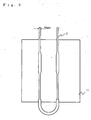
- Fig. 1 is a schematic sectional view showing a plasma CVD apparatus.
- a plurality of inductively coupled electrode 2 folded into U-shape with a diameter of 10mm or less, is placed in a deposition chamber 1 having a gas inlet 5 and an exhaust port 6.
- One end of electrode, a power feeding portion 9, is connected to a high-frequency power source 7 by a coaxial cable 8, and the other end, the grounded portion 10,
- the grounded portion 10 is connected to the wall of the deposition.
- the distance from the feeding portion 9 and grounded portion 10 to the turning portion 4 is preferably set to be nearly n/2 times (n: a natural number) of the excitation wavelength of the high-frequency power.
- n a natural number
- the turning portion is the semicircular portion having a curvature in the case of the U-shape electrode shown in Fig.1 .
- the inductively coupled electrode of this apparatus exemplified by Fig. 1 is constructed, for example, by bending a conductive rod or pipe having an outer diameter of 10 mm or less, made of stainless steel, Al, Cu or the like, into the U-shape.
- the electrode having a turning portion in a rectangular shape is also available. Moreover, the whole of electrode is not necessarily conductive. Therefore, the structure in which an insulator is covered with a conductor, for example, is also available.
- the electrode of center-folded shape in this invention is not limited to one that is constructed by bending, e.g., single rod or pipe. That is, the electrode having a structure in which two straight line electrodes are jointed and fixed with a metal plate or the like is also employed.
- the turning portion in the case of the rectangular shape is exemplified by a straight portion between the two straight line electrodes.
- the diameter of the electrode is partially 10 mm or less, between the feeding portion and the turning portion, the diameter of the rest of the electrode can be larger than 10mm. Therefore, the diameter may be constant over the entire electrode, or may be varied in the longitudinal direction; for example, the diameter can be gradually increased from the feeding portion toward the turning portion.
- the electrode diameter There is no limitation in the lower limit of the electrode diameter. So far as the electrode will not be broken down, enduring supplied power and stable discharge can be maintained, an extremely thin electrode can be employed. However, the electrode having a diameter of 1 - 10 mm is preferably employed from a viewpoint of handling and easy attachment.
- the glow discharge region can be expanded toward the end (or the turning portion) with smaller power by making the feeding side of the electrode thinner than 10mm. Consequently, a larger film formation region can be prepared, which makes film deposition on a large-sized substrate possible.
- the plasma density near the feeding portion is relatively decreased. That is, since the ratio of plasma density in the vicinity of power feeding portion to the film formation region becomes small, the energy is efficiently used for film formation, and therefore the amount of film deposited on inner wall near the power feeding portion will be decreased. Thus, since the repetition number of film deposition increases until the film deposited on the inner wall becomes so thick as to start peeling off, the maintenance cycle is remarkably extended and overall productivity is improved.
- reactive gases for deposition are introduced at a predetermined flow rate into deposition chamber 1 through gas inlet 5, and the pressure inside the deposition chamber is set to a predetermined value by adjusting the main valve (not shown) disposed in exhaust port 6.
- high frequency power is fed to power feeding portions 9 from high frequency power source 7.
- the frequency of high frequency is adjusted to establish a standing wave, resulting in the generation of the plasma along electrode 2.
- the plasma is expanded toward the electrode end (or the turning portion) along electrode 2 from the feeding portion and grounded portion.
- the reactive gases are decomposed and activated by the plasma to form a thin film with an excellent uniformity of film thickness on substrate 11 disposed in the position facing the electrodes 2.
- the electric discharge is further expanded toward the electrode end with smaller power by using the electrode whose diameter on power feeding side is 10 mm or less. Moreover, when the same power is fed, higher deposition rate is obtained for thinner electrode. Furthermore, since the plasma density near the power feeding portion becomes low, the amount of the film deposited on the inner wall will decrease.
- electrodes having a diameter of 10 mm or less on the power feeding side have been described.
- electrodes having a diameter more than 10 mm can also be employed if the diameter is varied in the longitudinal direction. That is, although the light and dark non-uniformities are partially observed in the plasma distribution when the electrode having a constant diameter and a center-folded shape is employed, the ratio of light and dark part of the plasma can be reduced to improve the uniformity of film thickness by varying the diameter, corresponding to the light and dark plasma position.
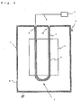
- Fig. 3 is a schematic sectional view showing the 2nd embodiment of the plasma CVD apparatus of this invention.
- the apparatus configuration is the same as that in Fig. 1 , except for the inductively coupled electrode 2.
- the surface of the electrode is covered with a dielectric 3 such as Teflon.
- the dielectric may be formed on entire surface of the electrode as shown in Fig. 3 , or partially. In any case, the film thickness uniformity can be improved. The position and shape of the dielectric are determined according to the pattern of plasma density distribution (or film thickness distribution).
- the peak in the film thickness distribution is reduced in intensity, which is considered to appear as a result of the interactive effect between the attenuation of high frequency power with propagation and the standing wave, and therefore the area having a prescribed uniformity of film thickness is expanded. Furthermore, the film thickness uniformity of the thin film can be further improved by changing the thickness of dielectric in the longitudinal direction of the electrode.
- the dielectric can be formed only on the power feeding side of the electrode as shown in Fig. 4 (a) , instead of the entire surface of electrode. In this configuration, the increase of the plasma density is suppressed on the power feeding portion side, which homogenizes the plasma density over the whole electrode to improve the film thickness uniformity.
- the electrode is provided with the dielectric only on the positions corresponding to high plasma density, more uniform film can be deposited in the longitudinal direction of the electrode.
- the dielectric When the dielectric becomes too thick, the plasma density may increase at the edge of dielectric, resulting in peak of the film thickness at the corresponding position of substrate.
- the dielectric preferably has a tapered edge in the cross-section, as shown in Fig. 4 (b) . That is, the thickness of dielectric is gradually decreased towards the end of dielectric. The uniformity of film thickness is further improved since the peak is prevented from generating at the position on the substrate corresponding to the edge.
- the dielectric may be wounded spirally around the longitudinal direction of the electrode as shown in Fig. 4 (c) , which averages the plasma density in the dielectric edge region and improves similarly the film thickness distribution.
- the thickness of dielectric is suitably determined, depending on the dielectric constant of material and the degree of plasma density distribution (film thickness distribution). In the case of, for example, Teflon, the preferable thickness is 0.1 mm or more.
- the dielectric any material that is stable to plasma and heat is employed. That is, organic materials such as Teflon or inorganic materials such as alumina and quartz are employed. However, the material having a large dielectric loss should be avoided.
- a straight line electrode can also be employed in stead of the electrode which is folded back shown in Fig. 1 .
- the power feeding portion and the grounded portion are fixed to the walls of the deposition chamber, facing to each other.
- n is a natural number.
- the electrode having a diameter of 10 mm or less partially or entirely between the power feeding portion and the grounded portion 2) the electrode having a varying diameter, and 3) the electrode covered with a dielectric.
- the 3rd embodiment of the plasma CVD apparatus of this invention is shown in Fig. 5 .
- a numeral 12 denotes a substrate holder.
- the phase of each electrode is not controlled, the film thickness distribution in the substrate widthwise direction is apt not to be uniform or reproducible. Furthermore, it is preferable to make anti-phase (that is, phase difference of 180 degrees) between adjacent electrodes. By reversing the phase of high frequency between adjacent electrodes, the thin film having a uniform thickness and characteristic can be formed over the entire substrate.
- the distance between the feeding portion and the turning portion (the distance between the feeding portion and the grounded portion for the straight line electrode) of alternate electrode may be elongated by a half wavelength of the high-frequency wave, and placing the feeding portions outside of the deposition chamber.
- coaxial cables equivalent to the half wavelength may be added to the feeding portions of alternate electrodes.
- a phase shifter may also be equipped to a high frequency power source to feed the high frequency power shifted by a half-wavelength to the feeling portions of the adjacent electrodes.
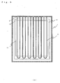
- FIG. 6 A preferred embodiment of the plasma CVD apparatus of this invention is shown in Fig. 6 .
- a plasma CVD apparatus of this embodiment further is characterized by arranging the electrode array, the plurality of electrodes arranged so as to cover substrate width as shown in Fig. 5 , in a plurality of layers with a predetermined interval, and that substrates are arranged on both sides of each layer.
- the simultaneous film formation on a number of substrates that is, six substrates in the case of drawing
- the distance between the electrode array and the substrate can be made as small as about 30 to 60 mm, it is possible to realize a thin film deposition apparatus which has a high throughput per floor space of the apparatus.
- the high frequency power source in a 30 - 300 MHz of VHF band is preferably employed.
- stainless steel or Cu rods or pipes having an outer diameter of 1, 4, 6 and 10mm were bent into U shape or folded into rectangular shape so as to have a distance of 30 mm between centers of rods or pipes and a length of 1570 mm.
- the feeding side surface of each electrode was covered with Teflons tube as shown in Fig. 4 (a) .
- Six electrodes were arranged to have a distance between center of rods or pipes of 30 mm in a common plane as shown in Fig. 5 .
- a substrate 11 of 1200mm x 500 mm was placed 40 mm apart from the electrode surface.
- the power feeding portions of the electrodes were connected to the connecting points of the feed through inside the deposition chamber and the grounded portions were connected to the inner wall of the chamber.
- the high frequency power was fed so that the phase was made in anti-phase between adjacent electrodes.
- the frequency was adjusted to establish a standing wave, and a-Si thin film was deposited on substrate 11.
- the electrode having an outer diameter of 1 mm was fabricated using a Cu wire and 2 mm thick Teflon. Stainless steel rods were employed and covered with 1 mm thick Teflon for fabricating electrodes having outer diameters of 4, 6, and 10 mm.
- the U-shape configuration was adopted for 1 mm and 10 mm electrodes, and the rectangularly folded shape was adopted for 4 mm and 6 mm electrodes.
- the discharge region was visibly observed for each electrode system with a variety of power supplied, which is shown in Table 1.
- the film thickness distributions were exemplified in Fig. 7 , which were measured in the longitudinal direction of the electrode at the central part of substrate.
- Fig. 7 shows the deposition rates when electrodes having a variety of diameters were used. In Fig. 7 , power supplied to each electrode was 25W for the 6 mm and 10 mm electrode, and the power was 13.75 W for the 4 mm electrode. As is apparent from the film thickness distribution of Fig.
- the uniform film thickness distribution can be obtained over a wide range by using an electrode having a diameter of 10mm or less and by feeding a predetermined power. Moreover, it has been found that higher deposition rate is obtained with the thinner electrode when the same power is supplied. It is likely from this point that the energy efficiency becomes higher as the electrode becomes thinner.
- the film thickness distribution is changed by covering the electrode with dielectric and by the power supply method, which will be described in this example.
- a-Si The film formation of a-Si was made on glass substrates using the plasma CVD apparatus shown in Fig. 5 .
- a stainless steel pipe having a diameter of 10mm was bent into U shape to have a distance of 30 mm between centers of the pipes and a length of 1570 mm, and the entire surface was then covered with Teflon tube of 1 mm in thickness.
- Six electrodes were arranged to have a distance between the center of the pipes of 30 mm in a common plane as shown in Fig. 5 .
- a substrate 11 of 1200mm x 500 mm was placed 40 mm apart from the electrode surface.
- the film thickness distributions were measured in the longitudinal direction of the electrode along the central part of substrate, which are shown in Fig. 8 .
- the film formations using electrodes which were not covered with dielectric were also carried out for comparison. These are also shown in Fig. 8 .
- the high frequency supply method and the electrode configuration shown in the diagram are as follows; (a) in-phase without dielectric, (b) anti-phase without dielectric, (c) in- phase with Teflon, and (d) anti-phase with Teflon.
- the horizontal axis denotes the position on the substrate in the longitudinal direction, and the vertical axis denotes the normalized film thickness.
- the film thickness distribution is greatly improved as compared with the prior art. Furthermore, it becomes possible to form a more uniform thin film even on a large-sized substrate having a size of 1200 mm or more by varying the thickness of dielectric in the longitudinal direction of the electrode, or by partially covering the electrode with a dielectric.
- the electric discharge region can be expanded in the longitudinal direction of electrode to form thin films on a larger substrate by a plasma CVD method of this invention; i.e., by supplying high frequency power on an inductively coupled electrode which has a diameter of 10 mm or less partially or entirely between the power feeding portion and the grounded portion and by generating the plasma so that a standing wave is established.
- the plasma is maintained with smaller power by employing thinner electrode.
- thinner electrode When the same power is supplied, higher deposition rate is obtained with thinner electrodes.
- the film deposition is decreased on the apparatus inner wall near power feeding portions, which greatly decreases cleaning frequency.
- the plasma density distribution can be partially adjusted in the longitudinal direction of the electrode, which makes it possible to form thin films with an excellent uniformity of film thickness.
- the arrangement of inductively coupled electrodes of this invention in a plurality of layers, with substrates on both sides of each layer can provide a plasma CVD apparatus and method of a high throughput.
Landscapes
- Chemical & Material Sciences (AREA)
- Engineering & Computer Science (AREA)
- Physics & Mathematics (AREA)
- Plasma & Fusion (AREA)
- Analytical Chemistry (AREA)
- Chemical Kinetics & Catalysis (AREA)
- General Chemical & Material Sciences (AREA)
- Materials Engineering (AREA)
- Mechanical Engineering (AREA)
- Metallurgy (AREA)
- Organic Chemistry (AREA)
- Plasma Technology (AREA)
- Chemical Vapour Deposition (AREA)
- Crystals, And After-Treatments Of Crystals (AREA)
- Fuel Cell (AREA)
Applications Claiming Priority (5)
| Application Number | Priority Date | Filing Date | Title |
|---|---|---|---|
| JP2000145645 | 2000-05-17 | ||
| JP2000145645 | 2000-05-17 | ||
| JP2000239221 | 2000-08-07 | ||
| JP2000239221 | 2000-08-07 | ||
| PCT/JP2001/004113 WO2001088221A1 (fr) | 2000-05-17 | 2001-05-17 | Appareil de depot chimique en phase vapeur (cvd) au plasma et procede associe |
Publications (4)
| Publication Number | Publication Date |
|---|---|
| EP1293588A1 EP1293588A1 (en) | 2003-03-19 |
| EP1293588A9 EP1293588A9 (en) | 2003-05-28 |
| EP1293588A4 EP1293588A4 (en) | 2007-03-28 |
| EP1293588B1 true EP1293588B1 (en) | 2009-12-16 |
Family
ID=26592083
Family Applications (1)
| Application Number | Title | Priority Date | Filing Date |
|---|---|---|---|
| EP01932112A Expired - Lifetime EP1293588B1 (en) | 2000-05-17 | 2001-05-17 | Plasma cvd apparatus and method |
Country Status (8)
| Country | Link |
|---|---|
| US (3) | US20040020432A1 (es) |
| EP (1) | EP1293588B1 (es) |
| JP (2) | JP4867124B2 (es) |
| KR (1) | KR100797423B1 (es) |
| AT (1) | ATE452219T1 (es) |
| DE (1) | DE60140803D1 (es) |
| ES (1) | ES2336303T3 (es) |
| WO (1) | WO2001088221A1 (es) |
Families Citing this family (26)
| Publication number | Priority date | Publication date | Assignee | Title |
|---|---|---|---|---|
| JP4509337B2 (ja) * | 2000-09-04 | 2010-07-21 | 株式会社Ihi | 薄膜形成方法及び薄膜形成装置 |
| JP4770029B2 (ja) * | 2001-01-22 | 2011-09-07 | 株式会社Ihi | プラズマcvd装置及び太陽電池の製造方法 |
| JP3820188B2 (ja) * | 2002-06-19 | 2006-09-13 | 三菱重工業株式会社 | プラズマ処理装置及びプラズマ処理方法 |
| JP2004055600A (ja) * | 2002-07-16 | 2004-02-19 | Tokyo Electron Ltd | プラズマ処理装置 |
| JP4120546B2 (ja) * | 2002-10-04 | 2008-07-16 | 株式会社Ihi | 薄膜形成方法及び装置並びに太陽電池の製造方法及び装置並びに太陽電池 |
| JP4741845B2 (ja) * | 2004-01-13 | 2011-08-10 | 株式会社 セルバック | 誘導結合プラズマ処理装置 |
| KR100858102B1 (ko) | 2004-03-26 | 2008-09-10 | 닛신덴키 가부시키 가이샤 | 플라즈마발생장치 |
| WO2007129568A1 (ja) * | 2006-05-01 | 2007-11-15 | Hitachi Kokusai Electric Inc. | 基板処理装置 |
| US7845310B2 (en) * | 2006-12-06 | 2010-12-07 | Axcelis Technologies, Inc. | Wide area radio frequency plasma apparatus for processing multiple substrates |
| WO2011137371A2 (en) * | 2010-04-30 | 2011-11-03 | Applied Materials, Inc. | Vertical inline cvd system |
| TW201233253A (en) * | 2011-01-26 | 2012-08-01 | Bing-Li Lai | Plasma reaction method and apparatus |
| WO2012176242A1 (ja) * | 2011-06-24 | 2012-12-27 | 日新電機株式会社 | プラズマ処理装置 |
| JP5780023B2 (ja) * | 2011-07-07 | 2015-09-16 | 株式会社Ihi | プラズマcvd装置およびプラズマcvd装置を用いた成膜方法 |
| GB2489761B (en) | 2011-09-07 | 2015-03-04 | Europlasma Nv | Surface coatings |
| JP5018994B1 (ja) | 2011-11-09 | 2012-09-05 | 日新電機株式会社 | プラズマ処理装置 |
| JP2013214445A (ja) * | 2012-04-03 | 2013-10-17 | Ihi Corp | プラズマ処理装置 |
| TWI502096B (zh) | 2013-06-17 | 2015-10-01 | Ind Tech Res Inst | 用於化學氣相沉積的反應裝置及反應製程 |
| FR3035881B1 (fr) * | 2015-05-04 | 2019-09-27 | Sidel Participations | Installation pour le traitement de recipients par plasma micro-ondes, comprenant un generateur a etat solide |
| JP6561725B2 (ja) * | 2015-09-25 | 2019-08-21 | 日新電機株式会社 | アンテナ及びプラズマ処理装置 |
| JP6870408B2 (ja) * | 2017-03-21 | 2021-05-12 | 日新電機株式会社 | プラズマ処理装置 |
| US11424104B2 (en) * | 2017-04-24 | 2022-08-23 | Applied Materials, Inc. | Plasma reactor with electrode filaments extending from ceiling |
| US11355321B2 (en) | 2017-06-22 | 2022-06-07 | Applied Materials, Inc. | Plasma reactor with electrode assembly for moving substrate |
| US11114284B2 (en) | 2017-06-22 | 2021-09-07 | Applied Materials, Inc. | Plasma reactor with electrode array in ceiling |
| US10510515B2 (en) | 2017-06-22 | 2019-12-17 | Applied Materials, Inc. | Processing tool with electrically switched electrode assembly |
| TWI788390B (zh) | 2017-08-10 | 2023-01-01 | 美商應用材料股份有限公司 | 用於電漿處理的分佈式電極陣列 |
| CN110364408A (zh) * | 2018-04-11 | 2019-10-22 | 北京北方华创微电子装备有限公司 | 电感耦合装置和等离子体处理设备 |
Family Cites Families (42)
| Publication number | Priority date | Publication date | Assignee | Title |
|---|---|---|---|---|
| JPS63276222A (ja) | 1987-05-08 | 1988-11-14 | Mitsubishi Electric Corp | 薄膜成長装置 |
| JPH0313578A (ja) | 1989-06-09 | 1991-01-22 | Mitsubishi Electric Corp | 薄膜形成装置 |
| US6068784A (en) * | 1989-10-03 | 2000-05-30 | Applied Materials, Inc. | Process used in an RF coupled plasma reactor |
| JPH03122274A (ja) | 1989-10-05 | 1991-05-24 | Asahi Glass Co Ltd | 薄膜製造方法および装置 |
| EP0428161B1 (en) * | 1989-11-15 | 1999-02-17 | Kokusai Electric Co., Ltd. | Dry process system |
| NL9000809A (nl) * | 1990-04-06 | 1991-11-01 | Philips Nv | Plasmagenerator. |
| JP2785442B2 (ja) | 1990-05-15 | 1998-08-13 | 三菱重工業株式会社 | プラズマcvd装置 |
| JP2989279B2 (ja) | 1991-01-21 | 1999-12-13 | 三菱重工業株式会社 | プラズマcvd装置 |
| US5324360A (en) * | 1991-05-21 | 1994-06-28 | Canon Kabushiki Kaisha | Method for producing non-monocrystalline semiconductor device and apparatus therefor |
| DE4136297A1 (de) | 1991-11-04 | 1993-05-06 | Plasma Electronic Gmbh, 7024 Filderstadt, De | Vorrichtung zur lokalen erzeugung eines plasmas in einer behandlungskammer mittels mikrowellenanregung |
| US5824158A (en) * | 1993-06-30 | 1998-10-20 | Kabushiki Kaisha Kobe Seiko Sho | Chemical vapor deposition using inductively coupled plasma and system therefor |
| JP3290777B2 (ja) * | 1993-09-10 | 2002-06-10 | 株式会社東芝 | 誘導結合型高周波放電方法および誘導結合型高周波放電装置 |
| JPH0794421A (ja) | 1993-09-21 | 1995-04-07 | Anelva Corp | アモルファスシリコン薄膜の製造方法 |
| US5571366A (en) * | 1993-10-20 | 1996-11-05 | Tokyo Electron Limited | Plasma processing apparatus |
| TW293983B (es) * | 1993-12-17 | 1996-12-21 | Tokyo Electron Co Ltd | |
| JP3424867B2 (ja) * | 1994-12-06 | 2003-07-07 | 富士通株式会社 | プラズマ処理装置及びプラズマ処理方法 |
| DE19503205C1 (de) | 1995-02-02 | 1996-07-11 | Muegge Electronic Gmbh | Vorrichtung zur Erzeugung von Plasma |
| JPH09106899A (ja) * | 1995-10-11 | 1997-04-22 | Anelva Corp | プラズマcvd装置及び方法並びにドライエッチング装置及び方法 |
| JP3268965B2 (ja) | 1995-10-13 | 2002-03-25 | 三洋電機株式会社 | 基板上に半導体膜を形成するための装置および方法 |
| US5965034A (en) * | 1995-12-04 | 1999-10-12 | Mc Electronics Co., Ltd. | High frequency plasma process wherein the plasma is executed by an inductive structure in which the phase and anti-phase portion of the capacitive currents between the inductive structure and the plasma are balanced |
| KR970064327A (ko) * | 1996-02-27 | 1997-09-12 | 모리시다 요이치 | 고주파 전력 인가장치, 플라즈마 발생장치, 플라즈마 처리장치, 고주파 전력 인가방법, 플라즈마 발생방법 및 플라즈마 처리방법 |
| JPH09268370A (ja) * | 1996-04-03 | 1997-10-14 | Canon Inc | プラズマcvd装置及びプラズマcvdによる堆積膜形成方法 |
| JP3544076B2 (ja) | 1996-08-22 | 2004-07-21 | キヤノン株式会社 | プラズマcvd装置およびプラズマcvdによる堆積膜形成方法 |
| JP3907087B2 (ja) * | 1996-10-28 | 2007-04-18 | キヤノンアネルバ株式会社 | プラズマ処理装置 |
| JPH11131244A (ja) | 1997-10-28 | 1999-05-18 | Canon Inc | プラズマ発生用高周波電極と、該電極により構成されたプラズマcvd装置及びプラズマcvd法 |
| JPH10265212A (ja) | 1997-03-26 | 1998-10-06 | Nippon Telegr & Teleph Corp <Ntt> | 微結晶および多結晶シリコン薄膜の製造方法 |
| EP1209721B1 (en) | 1997-10-10 | 2007-12-05 | European Community | Inductive type plasma processing chamber |
| EP0908921A1 (en) | 1997-10-10 | 1999-04-14 | European Community | Process chamber for plasma enhanced chemical vapour deposition and apparatus employing said process chamber |
| JP3501668B2 (ja) * | 1997-12-10 | 2004-03-02 | キヤノン株式会社 | プラズマcvd方法及びプラズマcvd装置 |
| WO1999031013A1 (en) * | 1997-12-15 | 1999-06-24 | Advanced Silicon Materials, Inc. | Chemical vapor deposition system for polycrystalline silicon rod production |
| DE19801366B4 (de) | 1998-01-16 | 2008-07-03 | Applied Materials Gmbh & Co. Kg | Vorrichtung zur Erzeugung von Plasma |
| JPH11317299A (ja) * | 1998-02-17 | 1999-11-16 | Toshiba Corp | 高周波放電方法及びその装置並びに高周波処理装置 |
| AU726151B2 (en) * | 1998-04-08 | 2000-11-02 | Mitsubishi Heavy Industries, Ltd. | Plasma CVD apparatus |
| JP3844274B2 (ja) | 1998-06-25 | 2006-11-08 | 独立行政法人産業技術総合研究所 | プラズマcvd装置及びプラズマcvd方法 |
| JP3572204B2 (ja) * | 1998-08-26 | 2004-09-29 | 三菱重工業株式会社 | プラズマcvd装置及び薄膜電子デバイス製造方法 |
| JP2000091236A (ja) * | 1998-09-08 | 2000-03-31 | Mitsubishi Heavy Ind Ltd | プラズマcvd装置 |
| JP2000232070A (ja) * | 1999-02-09 | 2000-08-22 | Canon Inc | 高周波プラズマcvd法 |
| JP2000345351A (ja) * | 1999-05-31 | 2000-12-12 | Anelva Corp | プラズマcvd装置 |
| JP3836636B2 (ja) | 1999-07-27 | 2006-10-25 | 独立行政法人科学技術振興機構 | プラズマ発生装置 |
| WO2001019144A1 (fr) * | 1999-09-09 | 2001-03-15 | Anelva Corporation | Dispositif de traitement au plasma a electrode interieure et procede associe |
| DE60134081D1 (de) * | 2000-04-13 | 2008-07-03 | Ihi Corp | Herstellungsverfahren von Dünnschichten, Gerät zur Herstellung von Dünnschichten und Sonnenzelle |
| JP4770029B2 (ja) * | 2001-01-22 | 2011-09-07 | 株式会社Ihi | プラズマcvd装置及び太陽電池の製造方法 |
-
2001
- 2001-05-17 ES ES01932112T patent/ES2336303T3/es not_active Expired - Lifetime
- 2001-05-17 US US10/276,371 patent/US20040020432A1/en not_active Abandoned
- 2001-05-17 KR KR1020027015416A patent/KR100797423B1/ko active IP Right Grant
- 2001-05-17 WO PCT/JP2001/004113 patent/WO2001088221A1/ja active Application Filing
- 2001-05-17 DE DE60140803T patent/DE60140803D1/de not_active Expired - Lifetime
- 2001-05-17 JP JP2001584602A patent/JP4867124B2/ja not_active Expired - Fee Related
- 2001-05-17 EP EP01932112A patent/EP1293588B1/en not_active Expired - Lifetime
- 2001-05-17 AT AT01932112T patent/ATE452219T1/de not_active IP Right Cessation
-
2009
- 2009-02-10 US US12/368,740 patent/US20090148624A1/en not_active Abandoned
-
2010
- 2010-08-13 US US12/855,809 patent/US9165748B2/en not_active Expired - Fee Related
-
2011
- 2011-07-08 JP JP2011151674A patent/JP5287944B2/ja not_active Expired - Lifetime
Also Published As
| Publication number | Publication date |
|---|---|
| KR20030032956A (ko) | 2003-04-26 |
| JP2012007239A (ja) | 2012-01-12 |
| WO2001088221A1 (fr) | 2001-11-22 |
| US20040020432A1 (en) | 2004-02-05 |
| JP5287944B2 (ja) | 2013-09-11 |
| US20090148624A1 (en) | 2009-06-11 |
| EP1293588A9 (en) | 2003-05-28 |
| US9165748B2 (en) | 2015-10-20 |
| EP1293588A4 (en) | 2007-03-28 |
| EP1293588A1 (en) | 2003-03-19 |
| JP4867124B2 (ja) | 2012-02-01 |
| KR100797423B1 (ko) | 2008-01-23 |
| ATE452219T1 (de) | 2010-01-15 |
| DE60140803D1 (de) | 2010-01-28 |
| US20100316815A1 (en) | 2010-12-16 |
| ES2336303T3 (es) | 2010-04-12 |
Similar Documents
| Publication | Publication Date | Title |
|---|---|---|
| US9165748B2 (en) | Plasma CVD method | |
| US6719876B1 (en) | Internal electrode type plasma processing apparatus and plasma processing method | |
| US4566403A (en) | Apparatus for microwave glow discharge deposition | |
| JP3332857B2 (ja) | 高周波プラズマ発生装置及び給電方法 | |
| KR100189311B1 (ko) | 플라즈마 발생용 마이크로파 플라즈마 토치 및 플라즈마 발생방법 | |
| KR100984659B1 (ko) | 플라즈마 처리 장치 | |
| US7976674B2 (en) | Embedded multi-inductive large area plasma source | |
| KR100757717B1 (ko) | 박막 형성 방법, 박막 형성 장치 및 태양전지 | |
| JP5017762B2 (ja) | 放電装置、プラズマ処理方法 | |
| WO2004031443A1 (ja) | 薄膜形成方法およびその装置 | |
| JP4474363B2 (ja) | マイクロ波プラズマ処理装置及びそのプラズマヘッド | |
| JP2004055600A (ja) | プラズマ処理装置 | |
| JP3907087B2 (ja) | プラズマ処理装置 | |
| US20090152243A1 (en) | Plasma processing apparatus and method thereof | |
| JP2000345351A (ja) | プラズマcvd装置 | |
| JP2002069653A (ja) | 薄膜形成方法、薄膜形成装置及び太陽電池 | |
| US20040163595A1 (en) | Plasma processing apparatus | |
| WO2009119241A1 (ja) | プラズマ処理装置 | |
| US7582185B2 (en) | Plasma-processing apparatus | |
| JP2001115265A (ja) | 高周波プラズマcvd法および高周波プラズマcvd装置 | |
| JP2004235380A (ja) | 表面処理装置および表面処理方法 | |
| JP4462461B2 (ja) | 薄膜形成方法、薄膜形成装置及び太陽電池 | |
| JP2004221571A (ja) | プラズマ処理装置 | |
| JPH10214700A (ja) | リニアプラズマ生成装置 |
Legal Events
| Date | Code | Title | Description |
|---|---|---|---|
| PUAI | Public reference made under article 153(3) epc to a published international application that has entered the european phase |
Free format text: ORIGINAL CODE: 0009012 |
|
| 17P | Request for examination filed |
Effective date: 20021129 |
|
| AK | Designated contracting states |
Kind code of ref document: A1 Designated state(s): AT BE CH CY DE DK ES FI FR GB GR IE IT LI LU MC NL PT SE TR |
|
| RAP1 | Party data changed (applicant data changed or rights of an application transferred) |
Owner name: ANELVA CORPORATION Owner name: ISHIKAWAJIMA-HARIMA HEAVY INDUSTRIES CO., LTD. |
|
| RIN1 | Information on inventor provided before grant (corrected) |
Inventor name: TAKAGI, TOMOKOC/O ISHIKAWAJIMA-HARIMA HEAVY IND. Inventor name: UEDA, HITOSHIC/O ISHIKAWAJIMA-HARIMA HEAVY IND. |
|
| RAP1 | Party data changed (applicant data changed or rights of an application transferred) |
Owner name: ISHIKAWAJIMA-HARIMA HEAVY INDUSTRIES CO., LTD. |
|
| RIN1 | Information on inventor provided before grant (corrected) |
Inventor name: UEDA, MASASHIC/O ISHIKAWAJIMA-HARIMA HEAVY IND. Inventor name: TAKAGI, TOMOKOC/O ISHIKAWAJIMA-HARIMA HEAVY IND. |
|
| RIN1 | Information on inventor provided before grant (corrected) |
Inventor name: TAKAGI, TOMOKOC/O ISHIKAWAJIMA-HARIMA HEAVY IND. Inventor name: UEDA, MASASHIC/O ISHIKAWAJIMA-HARIMA HEAVY IND. |
|
| A4 | Supplementary search report drawn up and despatched |
Effective date: 20070227 |
|
| 17Q | First examination report despatched |
Effective date: 20071001 |
|
| RAP1 | Party data changed (applicant data changed or rights of an application transferred) |
Owner name: IHI CORPORATION |
|
| GRAP | Despatch of communication of intention to grant a patent |
Free format text: ORIGINAL CODE: EPIDOSNIGR1 |
|
| GRAS | Grant fee paid |
Free format text: ORIGINAL CODE: EPIDOSNIGR3 |
|
| GRAA | (expected) grant |
Free format text: ORIGINAL CODE: 0009210 |
|
| AK | Designated contracting states |
Kind code of ref document: B1 Designated state(s): AT BE CH CY DE DK ES FI FR GB GR IE IT LI LU MC NL PT SE TR |
|
| REG | Reference to a national code |
Ref country code: GB Ref legal event code: FG4D |
|
| REG | Reference to a national code |
Ref country code: CH Ref legal event code: EP |
|
| REG | Reference to a national code |
Ref country code: IE Ref legal event code: FG4D |
|
| REF | Corresponds to: |
Ref document number: 60140803 Country of ref document: DE Date of ref document: 20100128 Kind code of ref document: P |
|
| REG | Reference to a national code |
Ref country code: ES Ref legal event code: FG2A Ref document number: 2336303 Country of ref document: ES Kind code of ref document: T3 |
|
| PG25 | Lapsed in a contracting state [announced via postgrant information from national office to epo] |
Ref country code: FI Free format text: LAPSE BECAUSE OF FAILURE TO SUBMIT A TRANSLATION OF THE DESCRIPTION OR TO PAY THE FEE WITHIN THE PRESCRIBED TIME-LIMIT Effective date: 20091216 Ref country code: SE Free format text: LAPSE BECAUSE OF FAILURE TO SUBMIT A TRANSLATION OF THE DESCRIPTION OR TO PAY THE FEE WITHIN THE PRESCRIBED TIME-LIMIT Effective date: 20091216 |
|
| PG25 | Lapsed in a contracting state [announced via postgrant information from national office to epo] |
Ref country code: AT Free format text: LAPSE BECAUSE OF FAILURE TO SUBMIT A TRANSLATION OF THE DESCRIPTION OR TO PAY THE FEE WITHIN THE PRESCRIBED TIME-LIMIT Effective date: 20091216 |
|
| PG25 | Lapsed in a contracting state [announced via postgrant information from national office to epo] |
Ref country code: PT Free format text: LAPSE BECAUSE OF FAILURE TO SUBMIT A TRANSLATION OF THE DESCRIPTION OR TO PAY THE FEE WITHIN THE PRESCRIBED TIME-LIMIT Effective date: 20100416 |
|
| PG25 | Lapsed in a contracting state [announced via postgrant information from national office to epo] |
Ref country code: BE Free format text: LAPSE BECAUSE OF FAILURE TO SUBMIT A TRANSLATION OF THE DESCRIPTION OR TO PAY THE FEE WITHIN THE PRESCRIBED TIME-LIMIT Effective date: 20091216 |
|
| PLBE | No opposition filed within time limit |
Free format text: ORIGINAL CODE: 0009261 |
|
| STAA | Information on the status of an ep patent application or granted ep patent |
Free format text: STATUS: NO OPPOSITION FILED WITHIN TIME LIMIT |
|
| PG25 | Lapsed in a contracting state [announced via postgrant information from national office to epo] |
Ref country code: GR Free format text: LAPSE BECAUSE OF FAILURE TO SUBMIT A TRANSLATION OF THE DESCRIPTION OR TO PAY THE FEE WITHIN THE PRESCRIBED TIME-LIMIT Effective date: 20100317 Ref country code: CY Free format text: LAPSE BECAUSE OF FAILURE TO SUBMIT A TRANSLATION OF THE DESCRIPTION OR TO PAY THE FEE WITHIN THE PRESCRIBED TIME-LIMIT Effective date: 20091216 |
|
| 26N | No opposition filed |
Effective date: 20100917 |
|
| PG25 | Lapsed in a contracting state [announced via postgrant information from national office to epo] |
Ref country code: MC Free format text: LAPSE BECAUSE OF NON-PAYMENT OF DUE FEES Effective date: 20100531 |
|
| PG25 | Lapsed in a contracting state [announced via postgrant information from national office to epo] |
Ref country code: DK Free format text: LAPSE BECAUSE OF FAILURE TO SUBMIT A TRANSLATION OF THE DESCRIPTION OR TO PAY THE FEE WITHIN THE PRESCRIBED TIME-LIMIT Effective date: 20091216 |
|
| PG25 | Lapsed in a contracting state [announced via postgrant information from national office to epo] |
Ref country code: IE Free format text: LAPSE BECAUSE OF NON-PAYMENT OF DUE FEES Effective date: 20100517 |
|
| PG25 | Lapsed in a contracting state [announced via postgrant information from national office to epo] |
Ref country code: LU Free format text: LAPSE BECAUSE OF NON-PAYMENT OF DUE FEES Effective date: 20100517 |
|
| PG25 | Lapsed in a contracting state [announced via postgrant information from national office to epo] |
Ref country code: TR Free format text: LAPSE BECAUSE OF FAILURE TO SUBMIT A TRANSLATION OF THE DESCRIPTION OR TO PAY THE FEE WITHIN THE PRESCRIBED TIME-LIMIT Effective date: 20091216 |
|
| REG | Reference to a national code |
Ref country code: DE Ref legal event code: R082 Ref document number: 60140803 Country of ref document: DE Representative=s name: MAI DOERR BESIER EUROPEAN PATENT ATTORNEYS - E, DE Ref country code: DE Ref legal event code: R082 Ref document number: 60140803 Country of ref document: DE Representative=s name: MAI DOERR BESIER PATENTANWAELTE, DE |
|
| REG | Reference to a national code |
Ref country code: FR Ref legal event code: PLFP Year of fee payment: 16 |
|
| REG | Reference to a national code |
Ref country code: FR Ref legal event code: PLFP Year of fee payment: 17 |
|
| REG | Reference to a national code |
Ref country code: FR Ref legal event code: PLFP Year of fee payment: 18 |
|
| PGFP | Annual fee paid to national office [announced via postgrant information from national office to epo] |
Ref country code: CH Payment date: 20200515 Year of fee payment: 20 Ref country code: ES Payment date: 20200601 Year of fee payment: 20 Ref country code: NL Payment date: 20200417 Year of fee payment: 20 Ref country code: FR Payment date: 20200414 Year of fee payment: 20 Ref country code: DE Payment date: 20200506 Year of fee payment: 20 |
|
| PGFP | Annual fee paid to national office [announced via postgrant information from national office to epo] |
Ref country code: GB Payment date: 20200506 Year of fee payment: 20 Ref country code: IT Payment date: 20200414 Year of fee payment: 20 |
|
| REG | Reference to a national code |
Ref country code: DE Ref legal event code: R071 Ref document number: 60140803 Country of ref document: DE |
|
| REG | Reference to a national code |
Ref country code: NL Ref legal event code: MK Effective date: 20210516 |
|
| REG | Reference to a national code |
Ref country code: CH Ref legal event code: PL |
|
| REG | Reference to a national code |
Ref country code: GB Ref legal event code: PE20 Expiry date: 20210516 |
|
| PG25 | Lapsed in a contracting state [announced via postgrant information from national office to epo] |
Ref country code: GB Free format text: LAPSE BECAUSE OF EXPIRATION OF PROTECTION Effective date: 20210516 |
|
| REG | Reference to a national code |
Ref country code: ES Ref legal event code: FD2A Effective date: 20220107 |
|
| PG25 | Lapsed in a contracting state [announced via postgrant information from national office to epo] |
Ref country code: ES Free format text: LAPSE BECAUSE OF EXPIRATION OF PROTECTION Effective date: 20210518 |