EP1253619B1 - Charged particle beam exposure apparatus and device manufacturing method using same - Google Patents
Charged particle beam exposure apparatus and device manufacturing method using same Download PDFInfo
- Publication number
- EP1253619B1 EP1253619B1 EP02252818A EP02252818A EP1253619B1 EP 1253619 B1 EP1253619 B1 EP 1253619B1 EP 02252818 A EP02252818 A EP 02252818A EP 02252818 A EP02252818 A EP 02252818A EP 1253619 B1 EP1253619 B1 EP 1253619B1
- Authority
- EP
- European Patent Office
- Prior art keywords
- charged particle
- electron
- array
- electron optical
- particle beam
- Prior art date
- Legal status (The legal status is an assumption and is not a legal conclusion. Google has not performed a legal analysis and makes no representation as to the accuracy of the status listed.)
- Expired - Lifetime
Links
- 239000002245 particle Substances 0.000 title claims description 36
- 238000004519 manufacturing process Methods 0.000 title claims description 13
- 230000003287 optical effect Effects 0.000 claims description 52
- 230000009467 reduction Effects 0.000 claims description 24
- 239000000758 substrate Substances 0.000 claims description 18
- 238000012937 correction Methods 0.000 claims description 14
- 101150111160 ALA1 gene Proteins 0.000 claims description 6
- 101150118692 ALS5 gene Proteins 0.000 claims description 6
- 101100177443 Spinacia oleracea HEMB gene Proteins 0.000 claims description 6
- 239000000463 material Substances 0.000 claims description 4
- 238000010894 electron beam technology Methods 0.000 description 58
- 238000000034 method Methods 0.000 description 17
- 230000004075 alteration Effects 0.000 description 11
- 239000004065 semiconductor Substances 0.000 description 8
- 230000008569 process Effects 0.000 description 6
- 238000007689 inspection Methods 0.000 description 4
- 201000009310 astigmatism Diseases 0.000 description 3
- 230000006870 function Effects 0.000 description 3
- 241000030538 Thecla Species 0.000 description 2
- 230000008901 benefit Effects 0.000 description 2
- 238000005530 etching Methods 0.000 description 2
- 150000002500 ions Chemical class 0.000 description 2
- 238000005259 measurement Methods 0.000 description 2
- 229910052710 silicon Inorganic materials 0.000 description 2
- 239000010703 silicon Substances 0.000 description 2
- 238000012360 testing method Methods 0.000 description 2
- 238000003491 array Methods 0.000 description 1
- 239000003795 chemical substances by application Substances 0.000 description 1
- 238000012790 confirmation Methods 0.000 description 1
- 239000013078 crystal Substances 0.000 description 1
- 230000007547 defect Effects 0.000 description 1
- 230000001419 dependent effect Effects 0.000 description 1
- 238000013461 design Methods 0.000 description 1
- 238000001514 detection method Methods 0.000 description 1
- 238000011161 development Methods 0.000 description 1
- 230000018109 developmental process Effects 0.000 description 1
- 238000010586 diagram Methods 0.000 description 1
- 238000006073 displacement reaction Methods 0.000 description 1
- 238000005538 encapsulation Methods 0.000 description 1
- 239000010408 film Substances 0.000 description 1
- 239000007943 implant Substances 0.000 description 1
- 239000012212 insulator Substances 0.000 description 1
- 230000010354 integration Effects 0.000 description 1
- 238000010884 ion-beam technique Methods 0.000 description 1
- 239000004973 liquid crystal related substance Substances 0.000 description 1
- 238000001459 lithography Methods 0.000 description 1
- 230000003647 oxidation Effects 0.000 description 1
- 238000007254 oxidation reaction Methods 0.000 description 1
- 238000012858 packaging process Methods 0.000 description 1
- 239000011295 pitch Substances 0.000 description 1
- 238000012545 processing Methods 0.000 description 1
- 238000012827 research and development Methods 0.000 description 1
- 239000003826 tablet Substances 0.000 description 1
- 239000010409 thin film Substances 0.000 description 1
- 238000007740 vapor deposition Methods 0.000 description 1
Images


Classifications
-
- H—ELECTRICITY
- H01—ELECTRIC ELEMENTS
- H01L—SEMICONDUCTOR DEVICES NOT COVERED BY CLASS H10
- H01L21/00—Processes or apparatus adapted for the manufacture or treatment of semiconductor or solid state devices or of parts thereof
- H01L21/02—Manufacture or treatment of semiconductor devices or of parts thereof
- H01L21/027—Making masks on semiconductor bodies for further photolithographic processing not provided for in group H01L21/18 or H01L21/34
-
- H—ELECTRICITY
- H01—ELECTRIC ELEMENTS
- H01J—ELECTRIC DISCHARGE TUBES OR DISCHARGE LAMPS
- H01J37/00—Discharge tubes with provision for introducing objects or material to be exposed to the discharge, e.g. for the purpose of examination or processing thereof
- H01J37/30—Electron-beam or ion-beam tubes for localised treatment of objects
- H01J37/317—Electron-beam or ion-beam tubes for localised treatment of objects for changing properties of the objects or for applying thin layers thereon, e.g. for ion implantation
- H01J37/3174—Particle-beam lithography, e.g. electron beam lithography
- H01J37/3177—Multi-beam, e.g. fly's eye, comb probe
-
- B—PERFORMING OPERATIONS; TRANSPORTING
- B82—NANOTECHNOLOGY
- B82Y—SPECIFIC USES OR APPLICATIONS OF NANOSTRUCTURES; MEASUREMENT OR ANALYSIS OF NANOSTRUCTURES; MANUFACTURE OR TREATMENT OF NANOSTRUCTURES
- B82Y10/00—Nanotechnology for information processing, storage or transmission, e.g. quantum computing or single electron logic
-
- B—PERFORMING OPERATIONS; TRANSPORTING
- B82—NANOTECHNOLOGY
- B82Y—SPECIFIC USES OR APPLICATIONS OF NANOSTRUCTURES; MEASUREMENT OR ANALYSIS OF NANOSTRUCTURES; MANUFACTURE OR TREATMENT OF NANOSTRUCTURES
- B82Y40/00—Manufacture or treatment of nanostructures
-
- H—ELECTRICITY
- H01—ELECTRIC ELEMENTS
- H01J—ELECTRIC DISCHARGE TUBES OR DISCHARGE LAMPS
- H01J37/00—Discharge tubes with provision for introducing objects or material to be exposed to the discharge, e.g. for the purpose of examination or processing thereof
- H01J37/02—Details
- H01J37/04—Arrangements of electrodes and associated parts for generating or controlling the discharge, e.g. electron-optical arrangement or ion-optical arrangement
- H01J37/045—Beam blanking or chopping, i.e. arrangements for momentarily interrupting exposure to the discharge
-
- H—ELECTRICITY
- H01—ELECTRIC ELEMENTS
- H01J—ELECTRIC DISCHARGE TUBES OR DISCHARGE LAMPS
- H01J2237/00—Discharge tubes exposing object to beam, e.g. for analysis treatment, etching, imaging
- H01J2237/04—Means for controlling the discharge
- H01J2237/043—Beam blanking
- H01J2237/0435—Multi-aperture
- H01J2237/0437—Semiconductor substrate
-
- H—ELECTRICITY
- H01—ELECTRIC ELEMENTS
- H01J—ELECTRIC DISCHARGE TUBES OR DISCHARGE LAMPS
- H01J2237/00—Discharge tubes exposing object to beam, e.g. for analysis treatment, etching, imaging
- H01J2237/30—Electron or ion beam tubes for processing objects
- H01J2237/317—Processing objects on a microscale
- H01J2237/3175—Lithography
- H01J2237/31774—Multi-beam
Definitions
- the present invention relates to a charged particle beam exposure apparatus, a device manufacturing method, and, more particularly, to a charged particle beam exposure apparatus for drawing a pattern on a substrate by using a plurality of charged particle beams, and a device manufacturing method using the same
- An example of an electron beam exposure apparatus includes, e.g., a point beam type apparatus which uses an electron beam formed into a spot, a variable shaped beam type apparatus which uses an electron beam formed into a variable-size rectangle, and a stencil mask type apparatus with which a stencil mask having a beam passing hole with a desired shape is formed in advance and which uses a beam formed into a desired shape with the stencil.
- the point beam type apparatus is suitable for forming a micropattern, it is used only for research and development as its throughput is very low.
- the variable shaped beam type apparatus has a throughput higher than that of the point beam type apparatus by one or two orders of magnitude. This throughput, however, is still low to draw a pattern in which micropatterns of about 100 nm are packed at a high integration degree.
- An example of a method that can draw any pattern includes an exposure method using a two-dimensional blanking aperture array (e.g., see Japanese Utility Model Publication No. 56-19402 ).
- a plurality of apertures for passing beams through them are two-dimensionally arranged in a large number in a semiconductor crystal substrate made of silicon or the like.
- a pair of blanking electrodes are formed on the two ends of each aperture, and whether to apply a voltage across the electrodes is controlled in accordance with pattern data.
- whether to cause the plurality of beams respectively passing through the plurality of apertures to travel linearly or to deflect them is controlled individually, thereby individually controlling whether the plurality of beams are to irradiate a sample.
- each aperture when one of the electrodes on the two ends of each aperture is grounded and a voltage is applied to the other electrode, the beam passing through this aperture is deflected. This beam is shielded by an aperture stop set under the blanking aperture array and does not irradiate the sample. If the voltage is not applied to the other electrode, the electron beam passing through the aperture is not deflected. This, the beam is not shielded by the aperture stop set under the blanking aperture array, and irradiates the sample surface.
- Fig. 9 schematically shows the arrangement of the two-dimensional blanking aperture array.
- a plurality of apertures (AP) are two-dimensionally arranged, and each aperture has a pair of electrodes (EL).
- the two-dimensional blanking array aperture has wiring lines and elements for individually controlling voltages to be applied to the electrodes of the plurality of apertures in accordance with pattern data.
- the apertures (AP) have diameters of 20 ⁇ m and are arranged with pitches of 100 ⁇ m.
- Each electrode (EL) has a thickness of 10 ⁇ m, a width of 10 ⁇ m, and a length (in the direction of depth) of about 50 ⁇ m.
- the spot size of the electron beam on the spot must be 25 nm or less.
- the sizes of the apertures of the blanker array are limited to 10 ⁇ m x 10 ⁇ m at minimum due to limitations in the manufacture.
- the reduction electron optical system To reduce the spot size of the electron beam, the shape of which is defined by such an aperture, with a reduction electron optical system to 25 nm or less, the reduction electron optical system must have a reduction magnification of 400 times, which is actually difficult to achieve.
- Document US-A-6 104 035 discloses an electron-beam exposure apparatus and method.
- the multi electron-beam exposure apparatus deflects a plurality of electron beams on an exposed surface, and upon each deflection, respectively controls irradiation of the respective electron beams.
- the apparatus writes a pattern by sequentially writing pattern parts of the pattern on subfields each composed of a plurality of elementary exposure fields, by simultaneously writing patterns on the respective elementary exposure fields.
- Pattern data of the pattern written on the exposed surface is divided in units of subfields, and as a control method for exposure of each subfield, a first control method to deflect the plurality of electron beams by a predetermined deflection width and set the electron beams, or a second control method to deflect the plurality of electron beams without setting the electron beams at positions where all the electron beams are cut off, is selected based on the divided pattern data for the subfield.
- a corresponding electron beam exposure apparatus having a source for emitting an electron beam and a reduction electron optical system for reducing and projecting, on a target exposure surface, an image of the source, includes a correction electron optical system which is arranged between the source and the reduction electron optical system to form a plurality of intermediate images of the source along a direction perpendicular to the optical axis of the reduction electron optical system, and corrects in advance aberrations generated when the intermediate images are reduced and projected on the target exposure surface by the reduction electron optical system
- the present invention has been made in view of the above situation, and one of its objects is to realize micropattern drawing without increasing the performance of a reduction electron optical system.
- An electron beam exposure apparatus will be shown as an example of an exposure apparatus that utilizes a charged particle beam. Note that the present invention is not limited to an exposure apparatus that uses an electron beam but can be similarly applied to, e.g., an exposure apparatus that uses an ion beam.
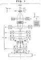
- Fig. 1 is a view showing the schematic arrangement of an electron beam exposure apparatus-according to a preferred embodiment of the present invention.
- This electron beam exposure apparatus adopts an electron gun 1 as a charged particle beam source.
- the electron gun 1 is constituted by a cathode 1a, grid 1b, and anode 1c. Electrons emitted from the cathode 1a form a cross-over image between the grid 1b and anode 1c. In the following description, this cross-over image is called an electron source ES.
- An electron beam emitted from the electron source ES is formed by a condenser lens optical system 2 into a substantially parallel electron beam, which then irradiates a multi-beam forming optical system 3.
- the condenser lens 2 is comprised of an electron lens (unipotential lens) made up of three aperture electrodes.
- the multi-beam forming optical system 3 is comprised of an aperture array AA, deflector array DA, lens array LA, blanker array BA, and correction lens array CLA sequentially arranged from the electron gun 1 side along an optical axis AX.
- the detailed arrangement of the multi-beam forming optical system 3 will be described later.
- the multi-beam forming optical system 3 forms a plurality of intermediate images of the electron source ES.
- the respective intermediate images are reduced and projected by a reduction electron optical system 4 -(to be described later) onto a wafer (sample) 5.
- the images of the electron source ES are formed on the wafer 5.
- the reduction electron optical system 4 is comprised of symmetric magnetic tablets constituted by a first projection lens 41 (43) and second projection lens 42 (44).
- the distance between the two lenses 41 and 42 is f1 + f2 where f1 is the focal length of the first projection lens 41 (43) and f2 is the focal length of the second projection lens 42 (44).
- the object point on the optical axis AX is located at the focal position of the first projection lens 41 (43), and the image point thereof is located at the focal position of the second projection lens 42 (44).
- the image is reduced to -f2/f1.
- Seidel aberrations excluding five aberrations i.e., spherical aberration, isotropic astigmatism, isotropic comatic aberration, curvature of field, and on-axis chromatic aberration, and chromatic aberrations concerning rotation and magnification are canceled.
- a deflector 6 deflects the plurality of electron beams from the multi-beam forming optical system 3 to displace the plurality of images of the electron source ES in the X and Y directions on the wafer 5 by substantially the same displacement amounts.
- the deflector 6 is comprised of a main deflector used when the deflection width is large, and a subdeflector used when the deflection width is small.
- the main deflector is typically an electromagnetic deflector
- the subdeflector is typically an electrostatic deflector.
- a dynamic focus coil 7 corrects an error in focal position of the image of the electron source ES which is caused by deflection aberration occurs when the deflector 6 is operated.
- a dynamic stigmatic coil 8 corrects astigmatism of the deflection aberration caused by deflection.
- a ⁇ -Z stage 9 places the wafer 5 on it and moves in the direction of the optical axis AX (Z-axis) and a rotational direction about the Z-axis.
- a stage reference plate 10 is fixed to the ⁇ -Z stage 9.
- An X-Y stage 11 moves the ⁇ -Z stage 9 in X and Y directions perpendicular to the optical axis AX (Z-axis).
- a reflected electron detector 12 detects reflected electrons produced when a mark on the stage reference plate 10 is irradiated with the electron beam.
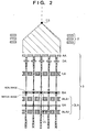
- the multi-beam forming optical system 3 mounted on the electron beam exposure apparatus shown in Fig. 1 will be described with reference to Fig. 2 .
- the multi-beam forming optical system 3 is typically comprised of the aperture array AA, deflector array DA, lens array LA, blanker array BA, and correction lens array CLA.
- the aperture array AA is formed of a substrate with a plurality of apertures.
- One electron beam which is made by the condenser lens 2 to be almost parallel is divided into a plurality of electron beams when it passes through the plurality of apertures.
- the deflector array DA is obtained by forming a plurality of deflectors, that individually deflect the plurality of electron beams divided by the aperture array AA, on one substrate.
- This substrate has a plurality of apertures.
- This substrate also has four pairs of electrodes arranged to sandwich the corresponding apertures. Namely, the apertures have eight deflection electrodes with deflecting functions.
- This substrate also has wiring lines for individually operating the deflection electrodes.
- the lens array LA is basically comprised of three substrates each having a plurality of aperture electrodes.
- One upper aperture electrode, one intermediate aperture electrode, and one lower aperture electrode form one electron lens (a so-called unipotential lens).
- the lens array LA has a plurality of electron lenses arrayed two-dimensionally. The same potential is applied to the upper, intermediate, and lower aperture electrodes so the plurality of electron lenses have the same optical characteristics (e.g., focal length).
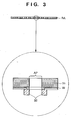
- the blanker array BA is obtained by forming a plurality of deflectors that individually deflect the plurality of electron beams on one substrate.
- Fig. 3 shows one of these deflectors in detail.
- a substrate 31 has apertures AP and pairs of deflection electrodes 32 each sandwiching the corresponding aperture AP.
- the substrate 31 also has wiring lines (W) for individually controlling the plurality of deflection electrodes 32, thereby individually controlling deflection of the plurality of electron beams.
- the correction lens array CLA is comprised of first and second electron lens arrays ALA1 and ALA2, each of which is an electron lens array formed by arranging a plurality of electron lenses two-dimensionally within one plane, and the stopper array SA.
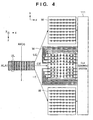
- Fig. 4 is a view for explaining the first electron optical system array ALA1.
- the first electron lens array ALA1 has three electrodes, i.e., upper, intermediate, and lower electrode plates UE, CE, and LE, each having a plurality of annular electrodes arranged in rows to correspond to the plurality of apertures.
- the three electrode plates are overlaid on each other through insulators.
- the annular electrodes with the same X and Y coordinates on the upper, intermediate, and lower electrode plates serve as one electron lens (a so-called unipotential lens) UL.
- All the annular electrodes of the upper and lower electrode plates of the respective electron lenses UL are connected to a CLA control circuit 111 through common wring lines (W), and are set at the same potential.
- W common wring lines
- the potentials of the upper and lower annular electrodes serve as electron beam accelerating potentials.
- the annular electrodes of the intermediate electrode plates of the respective electron lenses are connected to the CLA control circuit 111 through the individual wiring lines (W), and are set to desired potentials.
- the electron optical power (focal length) of each electron lens UL can be set to a desired value.
- the second electron lens array ALA2 has the same structure and function as those of the first electron lens array ALA1.
- the stopper array SA has the same structure as that of the aperture array AA.
- the function of the multi-beam forming optical system 3 will be described with reference to Fig. 2 .
- the substantially parallel electron beam passing through the condenser lens 2 is divided into a plurality of electron beams by the aperture array AA.
- the plurality of divided electron beams form a plurality of intermediate images of the electron source ES on the blanker array BA through the plurality of corresponding electron lenses of the lens array LA.
- the intermediate images depend not on the sizes of the apertures of the aperture array AA or of the apertures of the deflector array DA, but on the size of the electron source (cross-over image) ES.
- the size of the image of the electron source ES to be formed on the wafer 5 can be reduced to, e.g., 25 nm or less. Therefore, a micropattern with a line width of, e.g., 100 nm or less, can be drawn.
- the plurality of electron lenses of the lens array LA form the plurality of intermediate images (real images) of the electron source ES on substantially one plane (i.e., within or in the vicinity of the plane).
- the blanker array BA is arranged such that its deflection points are located on this plane.
- the plurality of electron beams passing through the plurality of apertures of the blanker array BA become incident on the reduction electron optical system 4 through the plurality of electron lenses of the correction lens array CLA corresponding to them.
- the respective electron lenses UL arranged in the correction lens array CLA form the virtual images of the plurality of intermediate images of the electron source ES formed within the plane of the blanker array BA. More specifically, the intermediate images of the electron source ES are formed at positions other than the front focal positions of the respective electron lenses UL each comprised of two lenses.
- the focal lengths of the two lenses that form each electron lens UL are adjusted such that the virtual images of the intermediate images (real images) are formed at positions where they cancel the curvature of field that occurs when the electron beams pass through the reduction electron optical system 4.
- the electron beams deflected by the blanker array BA are shielded by the stopper array SA formed in the correction lens array CLA and thus do not irradiate the wafer 5.
- the electron beams not deflected by the blanker array BA are not shielded by the stopper array SA formed in the correction lens array CLA and thus irradiate the wafer 5.
- the plurality of intermediate images are formed on substantially one plane and the blanker array BA is arranged such that its deflection points are located on this plane. Therefore, assuming that the stopper array SA does not exist, the electron beams deflected by the blanker array BA irradiate the positions on the wafer which are substantially same to the positions irradiated with the electron beams not deflected by the blanker array BA.
- Such a feature provides an advantage that the electron beams do not irradiate the undesirable portion on the wafer during ON/OFF-control of the election beams by the blanker array BA.
- a DA control circuit 110 individually controls the plurality of deflectors (deflection electrodes) that form the deflector array DA.
- the CLA control circuit 111 individually controls the focal lengths of the plurality of electron lenses UL that form the correction lens array CLA.
- the BA control circuit 112 individually controls ON/OFF of the plurality of blanking electrodes that form the blanker array BA.
- a D_STIG control circuit 113 controls the dynamic stigmatic coil 8 to control the astigmatism of the reduction electron optical system 4.
- a D_FOCUS control circuit 114 controls the dynamic focus coil 7 to control the focus of the reduction electron optical system 4.
- a deflection control circuit 115 controls the deflector 6.
- An optical characteristic control circuit 116 adjusts the optical characteristics (magnification, distortion) of the reduction electron optical system 4.
- a reflected electron detection circuit 117 calculates the amount of reflected electrons from a signal sent from the reflected electron detector 12.
- a stage drive control circuit 118 drive-controls the ⁇ -Z stage 9 and, in cooperation with a laser interferometer LIM that detects the position of the X-Y stage 11, the X-Y stage 11.
- a control system 120 reads out exposure control data from a memory 121 which stores it (e.g., including drawing pattern data), and controls the plurality of control circuits described above on the basis of the exposure control data.
- the control system 120 is controlled by a CPU 123 which controls the entire electron beam exposure apparatus through an interface 122.
- the control system 120 instructs the deflection control circuit 115 to deflect the plurality of electron beams with the deflector 6.
- the control system 120 also instructs the BA control circuit 112 to turn on/off the plurality of blanking electrodes of the blanker array BA individually in accordance with a pattern (drawing pattern data) to be drawn on the wafer 5.
- the X-Y stage 11 continuously moves in the Y direction.
- the plurality of electron beams are deflected by the deflector 6 to follow the movement of the X-Y stage 11.
- the electron beams scan and expose the corresponding element exposure regions (EF) on the wafer 5, as shown in Fig. 6 .
- the element exposure regions (EF) of the respective electron beams are adjacent to each other two-dimensionally. Consequently, a subfield (SF) constituted by the plurality of element exposure regions (EF) which are set to be exposed simultaneously is exposed simultaneously.
- SF subfield
- the control system 120 instructs the deflection control circuit 115 to deflect the plurality of electron beams by the deflector 6 in a direction (X direction) perpendicular to the stage scanning direction (Y direction), so that the next subfield (SF2) is exposed.
- the control system 120 instructs the BA control circuit 112, D_STIG control circuit 113, and D_FOCUS control circuit 114 to adjust the blanker array BA, dynamic stigmatic coil 8, and dynamic focus coil 7 so as to correct the changed aberration.
- the respective electron beams expose the corresponding element exposure regions (EF), thereby exposing the subfield 2 (SF2).
- subfields (SF1 to SF6) are sequentially exposed to expose a pattern onto the wafer 5.
- a main field (MF) constituted by the subfields (SF1 to SF6) arranged in a direction (X direction) perpendicular to the stage scanning direction (Y direction) is exposed on the wafer 5.
- the control system 120 instructs the deflection control circuit 115 to sequentially deflect the plurality of electron beams toward main fields (MF2, MF3, MF4,...) arranged in the stage scanning direction (Y direction), thus exposing them.
- a stripe (STRIPE1) constituted by the main fields (MF2, MF3, MF4,...) is exposed.
- the X-Y stage 11 is stepped in the X direction to expose the next stripe (STRIPE2).
- a device manufacturing method using the exposure apparatus according to the present invention represented by the electron beam exposure apparatus described above, will be described.
- Fig. 7 shows the flow of manufacture of a microdevice (a semiconductor chip such as an IC or LSI, a liquid crystal panel, a CCD, a thin film magnetic head, a micromachine, or the like).
- a semiconductor device circuit is designed.
- step 2 form exposure control data
- the exposure control data of the exposure apparatus is formed on the basis of the designed circuit pattern.
- step 3 manufactured by using a material such as silicon.
- step 4 wafer process
- a pre-process an actual circuit is formed on the wafer by lithography using the exposure apparatus, to which the prepared exposure control data has been input, and the wafer.
- step 5 assembly
- step 6 inspection
- step 7 inspections such as the operation confirmation test and durability test of the semiconductor device manufactured in step 5 are conducted. After these steps, the semiconductor device is completed, and shipped (step 7).
- Fig. 8 shows the detailed flow of the wafer process.
- step 11 oxidation
- step 12 CVD
- step 13 form electrode
- step 14 implant ion
- ions are implanted in the wafer.
- step 15 resist processing
- step 16 exposure
- step 18 etching
- step 19 etching
- Another application field of the present invention includes a charged particle beam applied apparatus, e.g., a length measurement apparatus for measuring the size of a pattern formed on a semiconductor substrate by using a plurality of charged particle beams generated by the arrangement as shown in Fig. 2 , a microscope apparatus for observing the pattern state, or an inspection apparatus for inspecting a pattern defect.
- a charged particle beam applied apparatus e.g., a length measurement apparatus for measuring the size of a pattern formed on a semiconductor substrate by using a plurality of charged particle beams generated by the arrangement as shown in Fig. 2 , a microscope apparatus for observing the pattern state, or an inspection apparatus for inspecting a pattern defect.
- a charged particle beam drawing apparatus that can draw a micropattern without increasing the performance of, e.g., a reduction electron optical system, can be provided. If a device is manufactured by using this apparatus, a device with higher precision than that with the prior art can be manufactured.
- length measurement, observation, and inspection can be performed within a short period of time with the plurality of generated charged particle beams.
Landscapes
- Engineering & Computer Science (AREA)
- Chemical & Material Sciences (AREA)
- Nanotechnology (AREA)
- Physics & Mathematics (AREA)
- Analytical Chemistry (AREA)
- Crystallography & Structural Chemistry (AREA)
- General Physics & Mathematics (AREA)
- Manufacturing & Machinery (AREA)
- Condensed Matter Physics & Semiconductors (AREA)
- Mathematical Physics (AREA)
- Theoretical Computer Science (AREA)
- Computer Hardware Design (AREA)
- Microelectronics & Electronic Packaging (AREA)
- Power Engineering (AREA)
- Electron Beam Exposure (AREA)
- Exposure And Positioning Against Photoresist Photosensitive Materials (AREA)
Applications Claiming Priority (2)
| Application Number | Priority Date | Filing Date | Title |
|---|---|---|---|
| JP2001124758 | 2001-04-23 | ||
| JP2001124758A JP4647820B2 (ja) | 2001-04-23 | 2001-04-23 | 荷電粒子線描画装置、および、デバイスの製造方法 |
Publications (3)
| Publication Number | Publication Date |
|---|---|
| EP1253619A2 EP1253619A2 (en) | 2002-10-30 |
| EP1253619A3 EP1253619A3 (en) | 2007-11-14 |
| EP1253619B1 true EP1253619B1 (en) | 2009-10-14 |
Family
ID=18974092
Family Applications (1)
| Application Number | Title | Priority Date | Filing Date |
|---|---|---|---|
| EP02252818A Expired - Lifetime EP1253619B1 (en) | 2001-04-23 | 2002-04-22 | Charged particle beam exposure apparatus and device manufacturing method using same |
Country Status (6)
| Country | Link |
|---|---|
| US (1) | US6903353B2 (ja) |
| EP (1) | EP1253619B1 (ja) |
| JP (1) | JP4647820B2 (ja) |
| KR (1) | KR100495651B1 (ja) |
| DE (1) | DE60233994D1 (ja) |
| TW (1) | TW559883B (ja) |
Families Citing this family (64)
| Publication number | Priority date | Publication date | Assignee | Title |
|---|---|---|---|---|
| JP3996267B2 (ja) * | 1998-05-12 | 2007-10-24 | エルピーダメモリ株式会社 | 半導体記憶装置 |
| JP2001284230A (ja) | 2000-03-31 | 2001-10-12 | Canon Inc | 電子光学系アレイ、これを用いた荷電粒子線露光装置ならびにデバイス製造方法 |
| JP2001283756A (ja) * | 2000-03-31 | 2001-10-12 | Canon Inc | 電子光学系アレイ、これを用いた荷電粒子線露光装置ならびにデバイス製造方法 |
| JP4947841B2 (ja) * | 2000-03-31 | 2012-06-06 | キヤノン株式会社 | 荷電粒子線露光装置 |
| JP4947842B2 (ja) * | 2000-03-31 | 2012-06-06 | キヤノン株式会社 | 荷電粒子線露光装置 |
| JP4585661B2 (ja) | 2000-03-31 | 2010-11-24 | キヤノン株式会社 | 電子光学系アレイ、荷電粒子線露光装置およびデバイス製造方法 |
| US6768125B2 (en) * | 2002-01-17 | 2004-07-27 | Ims Nanofabrication, Gmbh | Maskless particle-beam system for exposing a pattern on a substrate |
| US6953938B2 (en) * | 2002-10-03 | 2005-10-11 | Canon Kabushiki Kaisha | Deflector, method of manufacturing deflector, and charged particle beam exposure apparatus |
| US7098468B2 (en) * | 2002-11-07 | 2006-08-29 | Applied Materials, Inc. | Raster frame beam system for electron beam lithography |
| EP2293316B1 (en) * | 2003-02-14 | 2012-04-04 | Mapper Lithography IP B.V. | Dispenser cathode |
| JP4421836B2 (ja) * | 2003-03-28 | 2010-02-24 | キヤノン株式会社 | 露光装置及びデバイス製造方法 |
| CN100543920C (zh) * | 2003-05-28 | 2009-09-23 | 迈普尔平版印刷Ip有限公司 | 带电粒子小射束曝光系统 |
| JP4738723B2 (ja) * | 2003-08-06 | 2011-08-03 | キヤノン株式会社 | マルチ荷電粒子線描画装置、荷電粒子線の電流の測定方法及びデバイス製造方法 |
| EP1668662B1 (en) * | 2003-09-05 | 2012-10-31 | Carl Zeiss SMT GmbH | Particle-optical systems and arrangements and particle-optical components for such systems and arrangements |
| JP4313145B2 (ja) | 2003-10-07 | 2009-08-12 | 株式会社日立ハイテクノロジーズ | 荷電粒子ビーム描画方法及び荷電粒子ビーム描画装置 |
| DE10351059B4 (de) | 2003-10-31 | 2007-03-01 | Roth & Rau Ag | Verfahren und Vorrichtung zur Ionenstrahlbearbeitung von Oberflächen |
| GB2414111B (en) * | 2004-04-30 | 2010-01-27 | Ims Nanofabrication Gmbh | Advanced pattern definition for particle-beam processing |
| JP4477436B2 (ja) * | 2004-06-30 | 2010-06-09 | キヤノン株式会社 | 荷電粒子線露光装置 |
| JP4634076B2 (ja) * | 2004-06-30 | 2011-02-16 | キヤノン株式会社 | 荷電粒子線露光装置及びデバイス製造方法 |
| DE102004052995A1 (de) * | 2004-11-03 | 2006-05-11 | Leica Microsystems Lithography Gmbh | Vorrichtung zur Strukturierung eines Partikelstrahls |
| JP4657740B2 (ja) * | 2005-01-26 | 2011-03-23 | キヤノン株式会社 | 荷電粒子線光学系用収差測定装置、該収差測定装置を具備する荷電粒子線露光装置及び該装置を用いたデバイス製造方法 |
| WO2006084298A1 (en) * | 2005-02-11 | 2006-08-17 | Ims Nanofabrication Ag | Charged-particle exposure apparatus with electrostatic zone plate |
| JP4171479B2 (ja) | 2005-06-28 | 2008-10-22 | 株式会社日立ハイテクノロジーズ | 荷電粒子線応用装置及び荷電粒子線応用方法 |
| EP1941528B9 (en) * | 2005-09-06 | 2011-09-28 | Carl Zeiss SMT GmbH | Particle-optical arrangement with particle-optical component |
| EP2050118A1 (en) * | 2006-07-25 | 2009-04-22 | Mapper Lithography IP B.V. | A multiple beam charged particle optical system |
| US8134135B2 (en) * | 2006-07-25 | 2012-03-13 | Mapper Lithography Ip B.V. | Multiple beam charged particle optical system |
| EP2019415B1 (en) * | 2007-07-24 | 2016-05-11 | IMS Nanofabrication AG | Multi-beam source |
| JP5619629B2 (ja) * | 2008-02-26 | 2014-11-05 | マッパー・リソグラフィー・アイピー・ビー.ブイ. | 投影レンズ構成体 |
| JP5486163B2 (ja) * | 2008-03-19 | 2014-05-07 | 株式会社ニューフレアテクノロジー | 描画システム及び描画装置のパラメータ監視方法 |
| JP5587299B2 (ja) * | 2008-05-23 | 2014-09-10 | マッパー・リソグラフィー・アイピー・ビー.ブイ. | 結像システム |
| JP5634052B2 (ja) | 2009-01-09 | 2014-12-03 | キヤノン株式会社 | 荷電粒子線描画装置およびデバイス製造方法 |
| KR101714005B1 (ko) | 2010-07-13 | 2017-03-09 | 삼성전자 주식회사 | 광학 소자 및 이를 포함하는 노광 장치 |
| JP5463429B2 (ja) * | 2013-05-08 | 2014-04-09 | 株式会社ニューフレアテクノロジー | 荷電粒子描画システム及び荷電粒子描画装置のパラメータ監視方法 |
| CN106463347B (zh) * | 2014-06-13 | 2020-09-15 | 英特尔公司 | 即时电子束对准 |
| JP6553973B2 (ja) * | 2014-09-01 | 2019-07-31 | 株式会社ニューフレアテクノロジー | マルチ荷電粒子ビーム用のブランキング装置及びマルチ荷電粒子ビーム描画装置 |
| DE102015202172B4 (de) | 2015-02-06 | 2017-01-19 | Carl Zeiss Microscopy Gmbh | Teilchenstrahlsystem und Verfahren zur teilchenoptischen Untersuchung eines Objekts |
| JP6703092B2 (ja) | 2015-07-22 | 2020-06-03 | エーエスエムエル ネザーランズ ビー.ブイ. | 複数荷電粒子ビームの装置 |
| US11302511B2 (en) * | 2016-02-04 | 2022-04-12 | Kla Corporation | Field curvature correction for multi-beam inspection systems |
| US10418324B2 (en) | 2016-10-27 | 2019-09-17 | Asml Netherlands B.V. | Fabricating unique chips using a charged particle multi-beamlet lithography system |
| EP3559752A4 (en) * | 2016-12-23 | 2020-08-19 | ASML Netherlands B.V. | PRODUCTION OF UNIQUE CHIPS WITH A LITHOGRAPHY SYSTEM WITH MULTIPLE CARRIER PART JETS |
| US11062874B2 (en) * | 2016-12-30 | 2021-07-13 | Asml Netherlands B.V. | Apparatus using multiple charged particle beams |
| TWI742223B (zh) * | 2017-01-14 | 2021-10-11 | 美商克萊譚克公司 | 電子束系統及方法,以及掃描電子顯微鏡 |
| US10242839B2 (en) * | 2017-05-05 | 2019-03-26 | Kla-Tencor Corporation | Reduced Coulomb interactions in a multi-beam column |
| US10347460B2 (en) * | 2017-03-01 | 2019-07-09 | Dongfang Jingyuan Electron Limited | Patterned substrate imaging using multiple electron beams |
| US10176965B1 (en) * | 2017-07-05 | 2019-01-08 | ICT Integrated Circuit Testing Gesellschaft für Halbleiterprüftechnik mbH | Aberration-corrected multibeam source, charged particle beam device and method of imaging or illuminating a specimen with an array of primary charged particle beamlets |
| JP7286630B2 (ja) * | 2017-10-02 | 2023-06-05 | エーエスエムエル ネザーランズ ビー.ブイ. | 荷電粒子ビームを用いた装置 |
| JP6977528B2 (ja) | 2017-12-14 | 2021-12-08 | 株式会社ニューフレアテクノロジー | マルチビーム用アパーチャセット |
| DE102018202428B3 (de) | 2018-02-16 | 2019-05-09 | Carl Zeiss Microscopy Gmbh | Vielstrahl-Teilchenmikroskop |
| DE102018202421B3 (de) | 2018-02-16 | 2019-07-11 | Carl Zeiss Microscopy Gmbh | Vielstrahl-Teilchenstrahlsystem |
| WO2019166331A2 (en) | 2018-02-27 | 2019-09-06 | Carl Zeiss Microscopy Gmbh | Charged particle beam system and method |
| US10811215B2 (en) | 2018-05-21 | 2020-10-20 | Carl Zeiss Multisem Gmbh | Charged particle beam system |
| DE102018007455B4 (de) | 2018-09-21 | 2020-07-09 | Carl Zeiss Multisem Gmbh | Verfahren zum Detektorabgleich bei der Abbildung von Objekten mittels eines Mehrstrahl-Teilchenmikroskops, System sowie Computerprogrammprodukt |
| DE102018007652B4 (de) | 2018-09-27 | 2021-03-25 | Carl Zeiss Multisem Gmbh | Teilchenstrahl-System sowie Verfahren zur Stromregulierung von Einzel-Teilchenstrahlen |
| DE102018124044B3 (de) | 2018-09-28 | 2020-02-06 | Carl Zeiss Microscopy Gmbh | Verfahren zum Betreiben eines Vielstrahl-Teilchenstrahlmikroskops und Vielstrahl-Teilchenstrahlsystem |
| US11145485B2 (en) * | 2018-12-26 | 2021-10-12 | Nuflare Technology, Inc. | Multiple electron beams irradiation apparatus |
| KR102596926B1 (ko) * | 2018-12-31 | 2023-11-01 | 에이에스엠엘 네델란즈 비.브이. | 다중 빔 검사 장치 |
| TWI743626B (zh) | 2019-01-24 | 2021-10-21 | 德商卡爾蔡司多重掃描電子顯微鏡有限公司 | 包含多束粒子顯微鏡的系統、對3d樣本逐層成像之方法及電腦程式產品 |
| CN111477530B (zh) | 2019-01-24 | 2023-05-05 | 卡尔蔡司MultiSEM有限责任公司 | 利用多束粒子显微镜对3d样本成像的方法 |
| JP6954943B2 (ja) * | 2019-03-15 | 2021-10-27 | 日本電子株式会社 | 荷電粒子線装置 |
| DE102019005362A1 (de) | 2019-07-31 | 2021-02-04 | Carl Zeiss Multisem Gmbh | Verfahren zum Betreiben eines Vielzahl-Teilchenstrahlsystems unter Veränderung der numerischen Apertur, zugehöriges Computerprogrammprodukt und Vielzahl-Teilchenstrahlsystem |
| CA3163655A1 (en) | 2020-01-06 | 2021-07-15 | Marco Jan-Jaco Wieland | Charged particle assessment tool, inspection method |
| JP7409946B2 (ja) * | 2020-04-13 | 2024-01-09 | 株式会社ニューフレアテクノロジー | マルチ荷電粒子ビーム照射装置及びマルチ荷電粒子ビーム検査装置 |
| WO2024156469A1 (en) | 2023-01-25 | 2024-08-02 | Carl Zeiss Multisem Gmbh | Multi-beam particle microscope with improved multi-beam generator for field curvature correction and multi-beam generator |
| DE102023101774A1 (de) | 2023-01-25 | 2024-07-25 | Carl Zeiss Multisem Gmbh | Verfahren zum Auslegen eines Vielstrahl-Teilchenstrahlsystems mit monolithischen Bahnverlaufskorrekturplatten, Computerprogrammprodukt und Vielstrahl-Teilchenstrahlsystem |
Family Cites Families (24)
| Publication number | Priority date | Publication date | Assignee | Title |
|---|---|---|---|---|
| SE421832B (sv) | 1979-04-18 | 1982-02-01 | Pharos Ab | Anordning for att registrera topografin hos den chargerade massan i en masugn |
| JPH01295419A (ja) * | 1988-05-24 | 1989-11-29 | Fujitsu Ltd | 電子ビーム露光方法及びその装置 |
| US5830612A (en) * | 1996-01-24 | 1998-11-03 | Fujitsu Limited | Method of detecting a deficiency in a charged-particle-beam exposure mask |
| US5834783A (en) * | 1996-03-04 | 1998-11-10 | Canon Kabushiki Kaisha | Electron beam exposure apparatus and method, and device manufacturing method |
| JP3647128B2 (ja) * | 1996-03-04 | 2005-05-11 | キヤノン株式会社 | 電子ビーム露光装置とその露光方法 |
| JPH09320960A (ja) * | 1996-03-25 | 1997-12-12 | Nikon Corp | 荷電粒子線転写装置 |
| JP3927620B2 (ja) | 1996-06-12 | 2007-06-13 | キヤノン株式会社 | 電子ビーム露光方法及びそれを用いたデバイス製造方法 |
| US5929454A (en) | 1996-06-12 | 1999-07-27 | Canon Kabushiki Kaisha | Position detection apparatus, electron beam exposure apparatus, and methods associated with them |
| JP3796317B2 (ja) | 1996-06-12 | 2006-07-12 | キヤノン株式会社 | 電子ビーム露光方法及びそれを用いたデバイス製造方法 |
| JP3728015B2 (ja) | 1996-06-12 | 2005-12-21 | キヤノン株式会社 | 電子ビーム露光システム及びそれを用いたデバイス製造方法 |
| US5981954A (en) | 1997-01-16 | 1999-11-09 | Canon Kabushiki Kaisha | Electron beam exposure apparatus |
| JP3689516B2 (ja) | 1997-01-29 | 2005-08-31 | キヤノン株式会社 | 電子ビーム露光装置 |
| JPH10214779A (ja) | 1997-01-31 | 1998-08-11 | Canon Inc | 電子ビーム露光方法及び該方法を用いたデバイス製造方法 |
| US6107636A (en) | 1997-02-07 | 2000-08-22 | Canon Kabushiki Kaisha | Electron beam exposure apparatus and its control method |
| US6104035A (en) | 1997-06-02 | 2000-08-15 | Canon Kabushiki Kaisha | Electron-beam exposure apparatus and method |
| JPH10335223A (ja) * | 1997-06-02 | 1998-12-18 | Canon Inc | 電子ビーム露光方法及び電子ビーム露光装置 |
| JP3787417B2 (ja) | 1997-06-11 | 2006-06-21 | キヤノン株式会社 | 電子ビーム露光方法及び電子ビーム露光装置 |
| JPH11195590A (ja) * | 1998-01-05 | 1999-07-21 | Canon Inc | マルチ電子ビーム露光方法及び装置、ならびにデバイス製造方法 |
| US6157039A (en) * | 1998-05-07 | 2000-12-05 | Etec Systems, Inc. | Charged particle beam illumination of blanking aperture array |
| JP2000049071A (ja) | 1998-07-28 | 2000-02-18 | Canon Inc | 電子ビーム露光装置及び方法、ならびにデバイス製造方法 |
| JP2000093825A (ja) | 1998-09-21 | 2000-04-04 | Oomiya Seisakusho:Kk | 籾殻粉砕機 |
| JP2000251827A (ja) * | 1999-03-03 | 2000-09-14 | Nikon Corp | 照明光学系 |
| JP3859404B2 (ja) * | 1999-09-27 | 2006-12-20 | 株式会社東芝 | 荷電ビーム描画装置およびパターン描画方法並びに記録媒体 |
| US6566664B2 (en) * | 2000-03-17 | 2003-05-20 | Canon Kabushiki Kaisha | Charged-particle beam exposure apparatus and device manufacturing method |
-
2001
- 2001-04-23 JP JP2001124758A patent/JP4647820B2/ja not_active Expired - Fee Related
-
2002
- 2002-04-19 US US10/125,439 patent/US6903353B2/en not_active Expired - Lifetime
- 2002-04-22 TW TW091108248A patent/TW559883B/zh not_active IP Right Cessation
- 2002-04-22 DE DE60233994T patent/DE60233994D1/de not_active Expired - Lifetime
- 2002-04-22 KR KR10-2002-0021943A patent/KR100495651B1/ko not_active IP Right Cessation
- 2002-04-22 EP EP02252818A patent/EP1253619B1/en not_active Expired - Lifetime
Also Published As
| Publication number | Publication date |
|---|---|
| KR20020082769A (ko) | 2002-10-31 |
| US6903353B2 (en) | 2005-06-07 |
| JP4647820B2 (ja) | 2011-03-09 |
| EP1253619A3 (en) | 2007-11-14 |
| EP1253619A2 (en) | 2002-10-30 |
| JP2002319532A (ja) | 2002-10-31 |
| US20020160311A1 (en) | 2002-10-31 |
| TW559883B (en) | 2003-11-01 |
| KR100495651B1 (ko) | 2005-06-16 |
| DE60233994D1 (de) | 2009-11-26 |
Similar Documents
| Publication | Publication Date | Title |
|---|---|---|
| EP1253619B1 (en) | Charged particle beam exposure apparatus and device manufacturing method using same | |
| US6472672B1 (en) | Electron beam exposure apparatus and its control method | |
| US7005658B2 (en) | Charged particle beam exposure apparatus and method | |
| EP0794552B1 (en) | Electron beam exposure apparatus and method, and device manufacturing method | |
| US6137113A (en) | Electron beam exposure method and apparatus | |
| US6515409B2 (en) | Charged-particle beam exposure apparatus, exposure system, control method therefor, and device manufacturing method | |
| US6552353B1 (en) | Multi-electron beam exposure method and apparatus and device manufacturing method | |
| JPH1064812A (ja) | 電子ビーム露光方法及びそれを用いたデバイス製造方法 | |
| US6903352B2 (en) | Charged-particle beam exposure apparatus, charged-particle beam exposure method, control data determination method, and device manufacturing method using this method | |
| US6657210B1 (en) | Electron beam exposure method, a method of constructing exposure control data, and a computer-readable medium | |
| JPH1187206A (ja) | 電子ビーム露光装置及び該装置を用いたデバイス製造方法 | |
| JP5159035B2 (ja) | レンズアレイ及び該レンズアレイを含む荷電粒子線露光装置 | |
| US7049610B2 (en) | Charged particle beam exposure method, charged particle beam exposure apparatus, and device manufacturing method | |
| JP4018197B2 (ja) | 電子ビーム露光方法及び電子ビーム露光装置 | |
| US7005659B2 (en) | Charged particle beam exposure apparatus, charged particle beam exposure method, and device manufacturing method using the same apparatus | |
| JP4143204B2 (ja) | 荷電粒子線露光装置及び該装置を用いたデバイス製造方法 | |
| JPH09330870A (ja) | 電子ビーム露光装置及びその露光方法 | |
| JP3728315B2 (ja) | 電子ビーム露光装置、電子ビーム露光方法、および、デバイス製造方法 | |
| JP4006054B2 (ja) | 電子ビーム露光装置 | |
| JP2005032480A (ja) | 荷電粒子線露光装置および該装置を用いたデバイス製造方法 | |
| JPH10321509A (ja) | 電子ビーム露光方法及び電子ビーム露光装置 | |
| JP2007329221A (ja) | 荷電粒子線レンズアレイ、露光装置及びデバイス製造方法 | |
| JPH09330868A (ja) | 電子ビーム露光方法及びそれを用いたデバイス製造方法 | |
| JPH10214778A (ja) | 電子ビーム露光装置及び電子ビーム露光方法 | |
| JPH10321508A (ja) | 電子ビーム露光方法及び電子ビーム露光装置 |
Legal Events
| Date | Code | Title | Description |
|---|---|---|---|
| PUAI | Public reference made under article 153(3) epc to a published international application that has entered the european phase |
Free format text: ORIGINAL CODE: 0009012 |
|
| AK | Designated contracting states |
Kind code of ref document: A2 Designated state(s): AT BE CH CY DE DK ES FI FR GB GR IE IT LI LU MC NL PT SE TR |
|
| AX | Request for extension of the european patent |
Free format text: AL;LT;LV;MK;RO;SI |
|
| PUAL | Search report despatched |
Free format text: ORIGINAL CODE: 0009013 |
|
| AK | Designated contracting states |
Kind code of ref document: A3 Designated state(s): AT BE CH CY DE DK ES FI FR GB GR IE IT LI LU MC NL PT SE TR |
|
| AX | Request for extension of the european patent |
Extension state: AL LT LV MK RO SI |
|
| 17P | Request for examination filed |
Effective date: 20080328 |
|
| 17Q | First examination report despatched |
Effective date: 20080513 |
|
| AKX | Designation fees paid |
Designated state(s): DE GB NL |
|
| GRAP | Despatch of communication of intention to grant a patent |
Free format text: ORIGINAL CODE: EPIDOSNIGR1 |
|
| GRAS | Grant fee paid |
Free format text: ORIGINAL CODE: EPIDOSNIGR3 |
|
| GRAA | (expected) grant |
Free format text: ORIGINAL CODE: 0009210 |
|
| RIN1 | Information on inventor provided before grant (corrected) |
Inventor name: HASHIMOTO, SHINICHI Inventor name: SOHDA, YASUNARI, HITACHI, LTD., I.P.G Inventor name: MURAKI, MASATO |
|
| AK | Designated contracting states |
Kind code of ref document: B1 Designated state(s): DE GB NL |
|
| REG | Reference to a national code |
Ref country code: GB Ref legal event code: FG4D |
|
| REF | Corresponds to: |
Ref document number: 60233994 Country of ref document: DE Date of ref document: 20091126 Kind code of ref document: P |
|
| PLBE | No opposition filed within time limit |
Free format text: ORIGINAL CODE: 0009261 |
|
| STAA | Information on the status of an ep patent application or granted ep patent |
Free format text: STATUS: NO OPPOSITION FILED WITHIN TIME LIMIT |
|
| 26N | No opposition filed |
Effective date: 20100715 |
|
| GBPC | Gb: european patent ceased through non-payment of renewal fee |
Effective date: 20100422 |
|
| PG25 | Lapsed in a contracting state [announced via postgrant information from national office to epo] |
Ref country code: GB Free format text: LAPSE BECAUSE OF NON-PAYMENT OF DUE FEES Effective date: 20100422 |
|
| PGFP | Annual fee paid to national office [announced via postgrant information from national office to epo] |
Ref country code: NL Payment date: 20130416 Year of fee payment: 12 |
|
| REG | Reference to a national code |
Ref country code: NL Ref legal event code: V1 Effective date: 20141101 |
|
| PG25 | Lapsed in a contracting state [announced via postgrant information from national office to epo] |
Ref country code: NL Free format text: LAPSE BECAUSE OF NON-PAYMENT OF DUE FEES Effective date: 20141101 |
|
| REG | Reference to a national code |
Ref country code: DE Ref legal event code: R081 Ref document number: 60233994 Country of ref document: DE Owner name: ADVANTEST CORP., JP Free format text: FORMER OWNERS: CANON K.K., TOKYO, JP; HITACHI, LTD., TOKYO, JP; ADVANTEST CORP., TOKIO/TOKYO, JP Ref country code: DE Ref legal event code: R082 Ref document number: 60233994 Country of ref document: DE Representative=s name: TBK, DE |
|
| PGFP | Annual fee paid to national office [announced via postgrant information from national office to epo] |
Ref country code: DE Payment date: 20170420 Year of fee payment: 16 |
|
| REG | Reference to a national code |
Ref country code: DE Ref legal event code: R119 Ref document number: 60233994 Country of ref document: DE |
|
| PG25 | Lapsed in a contracting state [announced via postgrant information from national office to epo] |
Ref country code: DE Free format text: LAPSE BECAUSE OF NON-PAYMENT OF DUE FEES Effective date: 20181101 |