EP1253619B1 - Charged particle beam exposure apparatus and device manufacturing method using same - Google Patents
Charged particle beam exposure apparatus and device manufacturing method using same Download PDFInfo
- Publication number
- EP1253619B1 EP1253619B1 EP02252818A EP02252818A EP1253619B1 EP 1253619 B1 EP1253619 B1 EP 1253619B1 EP 02252818 A EP02252818 A EP 02252818A EP 02252818 A EP02252818 A EP 02252818A EP 1253619 B1 EP1253619 B1 EP 1253619B1
- Authority
- EP
- European Patent Office
- Prior art keywords
- charged particle
- electron
- array
- electron optical
- particle beam
- Prior art date
- Legal status (The legal status is an assumption and is not a legal conclusion. Google has not performed a legal analysis and makes no representation as to the accuracy of the status listed.)
- Expired - Lifetime
Links
Images


Classifications
-
- H—ELECTRICITY
- H01—ELECTRIC ELEMENTS
- H01L—SEMICONDUCTOR DEVICES NOT COVERED BY CLASS H10
- H01L21/00—Processes or apparatus adapted for the manufacture or treatment of semiconductor or solid state devices or of parts thereof
- H01L21/02—Manufacture or treatment of semiconductor devices or of parts thereof
- H01L21/027—Making masks on semiconductor bodies for further photolithographic processing not provided for in group H01L21/18 or H01L21/34
-
- H—ELECTRICITY
- H01—ELECTRIC ELEMENTS
- H01J—ELECTRIC DISCHARGE TUBES OR DISCHARGE LAMPS
- H01J37/00—Discharge tubes with provision for introducing objects or material to be exposed to the discharge, e.g. for the purpose of examination or processing thereof
- H01J37/30—Electron-beam or ion-beam tubes for localised treatment of objects
- H01J37/317—Electron-beam or ion-beam tubes for localised treatment of objects for changing properties of the objects or for applying thin layers thereon, e.g. for ion implantation
- H01J37/3174—Particle-beam lithography, e.g. electron beam lithography
- H01J37/3177—Multi-beam, e.g. fly's eye, comb probe
-
- B—PERFORMING OPERATIONS; TRANSPORTING
- B82—NANOTECHNOLOGY
- B82Y—SPECIFIC USES OR APPLICATIONS OF NANOSTRUCTURES; MEASUREMENT OR ANALYSIS OF NANOSTRUCTURES; MANUFACTURE OR TREATMENT OF NANOSTRUCTURES
- B82Y10/00—Nanotechnology for information processing, storage or transmission, e.g. quantum computing or single electron logic
-
- B—PERFORMING OPERATIONS; TRANSPORTING
- B82—NANOTECHNOLOGY
- B82Y—SPECIFIC USES OR APPLICATIONS OF NANOSTRUCTURES; MEASUREMENT OR ANALYSIS OF NANOSTRUCTURES; MANUFACTURE OR TREATMENT OF NANOSTRUCTURES
- B82Y40/00—Manufacture or treatment of nanostructures
-
- H—ELECTRICITY
- H01—ELECTRIC ELEMENTS
- H01J—ELECTRIC DISCHARGE TUBES OR DISCHARGE LAMPS
- H01J37/00—Discharge tubes with provision for introducing objects or material to be exposed to the discharge, e.g. for the purpose of examination or processing thereof
- H01J37/02—Details
- H01J37/04—Arrangements of electrodes and associated parts for generating or controlling the discharge, e.g. electron-optical arrangement, ion-optical arrangement
- H01J37/045—Beam blanking or chopping, i.e. arrangements for momentarily interrupting exposure to the discharge
-
- H—ELECTRICITY
- H01—ELECTRIC ELEMENTS
- H01J—ELECTRIC DISCHARGE TUBES OR DISCHARGE LAMPS
- H01J2237/00—Discharge tubes exposing object to beam, e.g. for analysis treatment, etching, imaging
- H01J2237/04—Means for controlling the discharge
- H01J2237/043—Beam blanking
- H01J2237/0435—Multi-aperture
- H01J2237/0437—Semiconductor substrate
-
- H—ELECTRICITY
- H01—ELECTRIC ELEMENTS
- H01J—ELECTRIC DISCHARGE TUBES OR DISCHARGE LAMPS
- H01J2237/00—Discharge tubes exposing object to beam, e.g. for analysis treatment, etching, imaging
- H01J2237/30—Electron or ion beam tubes for processing objects
- H01J2237/317—Processing objects on a microscale
- H01J2237/3175—Lithography
- H01J2237/31774—Multi-beam
Definitions
- the present invention relates to a charged particle beam exposure apparatus, a device manufacturing method, and, more particularly, to a charged particle beam exposure apparatus for drawing a pattern on a substrate by using a plurality of charged particle beams, and a device manufacturing method using the same
- An example of an electron beam exposure apparatus includes, e.g., a point beam type apparatus which uses an electron beam formed into a spot, a variable shaped beam type apparatus which uses an electron beam formed into a variable-size rectangle, and a stencil mask type apparatus with which a stencil mask having a beam passing hole with a desired shape is formed in advance and which uses a beam formed into a desired shape with the stencil.
- the point beam type apparatus is suitable for forming a micropattern, it is used only for research and development as its throughput is very low.
- the variable shaped beam type apparatus has a throughput higher than that of the point beam type apparatus by one or two orders of magnitude. This throughput, however, is still low to draw a pattern in which micropatterns of about 100 nm are packed at a high integration degree.
- An example of a method that can draw any pattern includes an exposure method using a two-dimensional blanking aperture array (e.g., see Japanese Utility Model Publication No. 56-19402 ).
- a plurality of apertures for passing beams through them are two-dimensionally arranged in a large number in a semiconductor crystal substrate made of silicon or the like.
- a pair of blanking electrodes are formed on the two ends of each aperture, and whether to apply a voltage across the electrodes is controlled in accordance with pattern data.
- whether to cause the plurality of beams respectively passing through the plurality of apertures to travel linearly or to deflect them is controlled individually, thereby individually controlling whether the plurality of beams are to irradiate a sample.
- each aperture when one of the electrodes on the two ends of each aperture is grounded and a voltage is applied to the other electrode, the beam passing through this aperture is deflected. This beam is shielded by an aperture stop set under the blanking aperture array and does not irradiate the sample. If the voltage is not applied to the other electrode, the electron beam passing through the aperture is not deflected. This, the beam is not shielded by the aperture stop set under the blanking aperture array, and irradiates the sample surface.
- Fig. 9 schematically shows the arrangement of the two-dimensional blanking aperture array.
- a plurality of apertures (AP) are two-dimensionally arranged, and each aperture has a pair of electrodes (EL).
- the two-dimensional blanking array aperture has wiring lines and elements for individually controlling voltages to be applied to the electrodes of the plurality of apertures in accordance with pattern data.
- the apertures (AP) have diameters of 20 ⁇ m and are arranged with pitches of 100 ⁇ m.
- Each electrode (EL) has a thickness of 10 ⁇ m, a width of 10 ⁇ m, and a length (in the direction of depth) of about 50 ⁇ m.
- the spot size of the electron beam on the spot must be 25 nm or less.
- the sizes of the apertures of the blanker array are limited to 10 ⁇ m x 10 ⁇ m at minimum due to limitations in the manufacture.
- the reduction electron optical system To reduce the spot size of the electron beam, the shape of which is defined by such an aperture, with a reduction electron optical system to 25 nm or less, the reduction electron optical system must have a reduction magnification of 400 times, which is actually difficult to achieve.
- Document US-A-6 104 035 discloses an electron-beam exposure apparatus and method.
- the multi electron-beam exposure apparatus deflects a plurality of electron beams on an exposed surface, and upon each deflection, respectively controls irradiation of the respective electron beams.
- the apparatus writes a pattern by sequentially writing pattern parts of the pattern on subfields each composed of a plurality of elementary exposure fields, by simultaneously writing patterns on the respective elementary exposure fields.
- Pattern data of the pattern written on the exposed surface is divided in units of subfields, and as a control method for exposure of each subfield, a first control method to deflect the plurality of electron beams by a predetermined deflection width and set the electron beams, or a second control method to deflect the plurality of electron beams without setting the electron beams at positions where all the electron beams are cut off, is selected based on the divided pattern data for the subfield.
- a corresponding electron beam exposure apparatus having a source for emitting an electron beam and a reduction electron optical system for reducing and projecting, on a target exposure surface, an image of the source, includes a correction electron optical system which is arranged between the source and the reduction electron optical system to form a plurality of intermediate images of the source along a direction perpendicular to the optical axis of the reduction electron optical system, and corrects in advance aberrations generated when the intermediate images are reduced and projected on the target exposure surface by the reduction electron optical system
- the present invention has been made in view of the above situation, and one of its objects is to realize micropattern drawing without increasing the performance of a reduction electron optical system.
- An electron beam exposure apparatus will be shown as an example of an exposure apparatus that utilizes a charged particle beam. Note that the present invention is not limited to an exposure apparatus that uses an electron beam but can be similarly applied to, e.g., an exposure apparatus that uses an ion beam.
- Fig. 1 is a view showing the schematic arrangement of an electron beam exposure apparatus-according to a preferred embodiment of the present invention.
- This electron beam exposure apparatus adopts an electron gun 1 as a charged particle beam source.
- the electron gun 1 is constituted by a cathode 1a, grid 1b, and anode 1c. Electrons emitted from the cathode 1a form a cross-over image between the grid 1b and anode 1c. In the following description, this cross-over image is called an electron source ES.
- An electron beam emitted from the electron source ES is formed by a condenser lens optical system 2 into a substantially parallel electron beam, which then irradiates a multi-beam forming optical system 3.
- the condenser lens 2 is comprised of an electron lens (unipotential lens) made up of three aperture electrodes.
- the multi-beam forming optical system 3 is comprised of an aperture array AA, deflector array DA, lens array LA, blanker array BA, and correction lens array CLA sequentially arranged from the electron gun 1 side along an optical axis AX.
- the detailed arrangement of the multi-beam forming optical system 3 will be described later.
- the multi-beam forming optical system 3 forms a plurality of intermediate images of the electron source ES.
- the respective intermediate images are reduced and projected by a reduction electron optical system 4 -(to be described later) onto a wafer (sample) 5.
- the images of the electron source ES are formed on the wafer 5.
- the reduction electron optical system 4 is comprised of symmetric magnetic tablets constituted by a first projection lens 41 (43) and second projection lens 42 (44).
- the distance between the two lenses 41 and 42 is f1 + f2 where f1 is the focal length of the first projection lens 41 (43) and f2 is the focal length of the second projection lens 42 (44).
- the object point on the optical axis AX is located at the focal position of the first projection lens 41 (43), and the image point thereof is located at the focal position of the second projection lens 42 (44).
- the image is reduced to -f2/f1.
- Seidel aberrations excluding five aberrations i.e., spherical aberration, isotropic astigmatism, isotropic comatic aberration, curvature of field, and on-axis chromatic aberration, and chromatic aberrations concerning rotation and magnification are canceled.
- a deflector 6 deflects the plurality of electron beams from the multi-beam forming optical system 3 to displace the plurality of images of the electron source ES in the X and Y directions on the wafer 5 by substantially the same displacement amounts.
- the deflector 6 is comprised of a main deflector used when the deflection width is large, and a subdeflector used when the deflection width is small.
- the main deflector is typically an electromagnetic deflector
- the subdeflector is typically an electrostatic deflector.
- a dynamic focus coil 7 corrects an error in focal position of the image of the electron source ES which is caused by deflection aberration occurs when the deflector 6 is operated.
- a dynamic stigmatic coil 8 corrects astigmatism of the deflection aberration caused by deflection.
- a ⁇ -Z stage 9 places the wafer 5 on it and moves in the direction of the optical axis AX (Z-axis) and a rotational direction about the Z-axis.
- a stage reference plate 10 is fixed to the ⁇ -Z stage 9.
- An X-Y stage 11 moves the ⁇ -Z stage 9 in X and Y directions perpendicular to the optical axis AX (Z-axis).
- a reflected electron detector 12 detects reflected electrons produced when a mark on the stage reference plate 10 is irradiated with the electron beam.
- the multi-beam forming optical system 3 mounted on the electron beam exposure apparatus shown in Fig. 1 will be described with reference to Fig. 2 .
- the multi-beam forming optical system 3 is typically comprised of the aperture array AA, deflector array DA, lens array LA, blanker array BA, and correction lens array CLA.
- the aperture array AA is formed of a substrate with a plurality of apertures.
- One electron beam which is made by the condenser lens 2 to be almost parallel is divided into a plurality of electron beams when it passes through the plurality of apertures.
- the deflector array DA is obtained by forming a plurality of deflectors, that individually deflect the plurality of electron beams divided by the aperture array AA, on one substrate.
- This substrate has a plurality of apertures.
- This substrate also has four pairs of electrodes arranged to sandwich the corresponding apertures. Namely, the apertures have eight deflection electrodes with deflecting functions.
- This substrate also has wiring lines for individually operating the deflection electrodes.
- the lens array LA is basically comprised of three substrates each having a plurality of aperture electrodes.
- One upper aperture electrode, one intermediate aperture electrode, and one lower aperture electrode form one electron lens (a so-called unipotential lens).
- the lens array LA has a plurality of electron lenses arrayed two-dimensionally. The same potential is applied to the upper, intermediate, and lower aperture electrodes so the plurality of electron lenses have the same optical characteristics (e.g., focal length).
- the blanker array BA is obtained by forming a plurality of deflectors that individually deflect the plurality of electron beams on one substrate.
- Fig. 3 shows one of these deflectors in detail.
- a substrate 31 has apertures AP and pairs of deflection electrodes 32 each sandwiching the corresponding aperture AP.
- the substrate 31 also has wiring lines (W) for individually controlling the plurality of deflection electrodes 32, thereby individually controlling deflection of the plurality of electron beams.
- the correction lens array CLA is comprised of first and second electron lens arrays ALA1 and ALA2, each of which is an electron lens array formed by arranging a plurality of electron lenses two-dimensionally within one plane, and the stopper array SA.
- Fig. 4 is a view for explaining the first electron optical system array ALA1.
- the first electron lens array ALA1 has three electrodes, i.e., upper, intermediate, and lower electrode plates UE, CE, and LE, each having a plurality of annular electrodes arranged in rows to correspond to the plurality of apertures.
- the three electrode plates are overlaid on each other through insulators.
- the annular electrodes with the same X and Y coordinates on the upper, intermediate, and lower electrode plates serve as one electron lens (a so-called unipotential lens) UL.
- All the annular electrodes of the upper and lower electrode plates of the respective electron lenses UL are connected to a CLA control circuit 111 through common wring lines (W), and are set at the same potential.
- W common wring lines
- the potentials of the upper and lower annular electrodes serve as electron beam accelerating potentials.
- the annular electrodes of the intermediate electrode plates of the respective electron lenses are connected to the CLA control circuit 111 through the individual wiring lines (W), and are set to desired potentials.
- the electron optical power (focal length) of each electron lens UL can be set to a desired value.
- the second electron lens array ALA2 has the same structure and function as those of the first electron lens array ALA1.
- the stopper array SA has the same structure as that of the aperture array AA.
- the function of the multi-beam forming optical system 3 will be described with reference to Fig. 2 .
- the substantially parallel electron beam passing through the condenser lens 2 is divided into a plurality of electron beams by the aperture array AA.
- the plurality of divided electron beams form a plurality of intermediate images of the electron source ES on the blanker array BA through the plurality of corresponding electron lenses of the lens array LA.
- the intermediate images depend not on the sizes of the apertures of the aperture array AA or of the apertures of the deflector array DA, but on the size of the electron source (cross-over image) ES.
- the size of the image of the electron source ES to be formed on the wafer 5 can be reduced to, e.g., 25 nm or less. Therefore, a micropattern with a line width of, e.g., 100 nm or less, can be drawn.
- the plurality of electron lenses of the lens array LA form the plurality of intermediate images (real images) of the electron source ES on substantially one plane (i.e., within or in the vicinity of the plane).
- the blanker array BA is arranged such that its deflection points are located on this plane.
- the plurality of electron beams passing through the plurality of apertures of the blanker array BA become incident on the reduction electron optical system 4 through the plurality of electron lenses of the correction lens array CLA corresponding to them.
- the respective electron lenses UL arranged in the correction lens array CLA form the virtual images of the plurality of intermediate images of the electron source ES formed within the plane of the blanker array BA. More specifically, the intermediate images of the electron source ES are formed at positions other than the front focal positions of the respective electron lenses UL each comprised of two lenses.
- the focal lengths of the two lenses that form each electron lens UL are adjusted such that the virtual images of the intermediate images (real images) are formed at positions where they cancel the curvature of field that occurs when the electron beams pass through the reduction electron optical system 4.
- the electron beams deflected by the blanker array BA are shielded by the stopper array SA formed in the correction lens array CLA and thus do not irradiate the wafer 5.
- the electron beams not deflected by the blanker array BA are not shielded by the stopper array SA formed in the correction lens array CLA and thus irradiate the wafer 5.
- the plurality of intermediate images are formed on substantially one plane and the blanker array BA is arranged such that its deflection points are located on this plane. Therefore, assuming that the stopper array SA does not exist, the electron beams deflected by the blanker array BA irradiate the positions on the wafer which are substantially same to the positions irradiated with the electron beams not deflected by the blanker array BA.
- Such a feature provides an advantage that the electron beams do not irradiate the undesirable portion on the wafer during ON/OFF-control of the election beams by the blanker array BA.
- a DA control circuit 110 individually controls the plurality of deflectors (deflection electrodes) that form the deflector array DA.
- the CLA control circuit 111 individually controls the focal lengths of the plurality of electron lenses UL that form the correction lens array CLA.
- the BA control circuit 112 individually controls ON/OFF of the plurality of blanking electrodes that form the blanker array BA.
- a D_STIG control circuit 113 controls the dynamic stigmatic coil 8 to control the astigmatism of the reduction electron optical system 4.
- a D_FOCUS control circuit 114 controls the dynamic focus coil 7 to control the focus of the reduction electron optical system 4.
- a deflection control circuit 115 controls the deflector 6.
- An optical characteristic control circuit 116 adjusts the optical characteristics (magnification, distortion) of the reduction electron optical system 4.
- a reflected electron detection circuit 117 calculates the amount of reflected electrons from a signal sent from the reflected electron detector 12.
- a stage drive control circuit 118 drive-controls the ⁇ -Z stage 9 and, in cooperation with a laser interferometer LIM that detects the position of the X-Y stage 11, the X-Y stage 11.
- a control system 120 reads out exposure control data from a memory 121 which stores it (e.g., including drawing pattern data), and controls the plurality of control circuits described above on the basis of the exposure control data.
- the control system 120 is controlled by a CPU 123 which controls the entire electron beam exposure apparatus through an interface 122.
- the control system 120 instructs the deflection control circuit 115 to deflect the plurality of electron beams with the deflector 6.
- the control system 120 also instructs the BA control circuit 112 to turn on/off the plurality of blanking electrodes of the blanker array BA individually in accordance with a pattern (drawing pattern data) to be drawn on the wafer 5.
- the X-Y stage 11 continuously moves in the Y direction.
- the plurality of electron beams are deflected by the deflector 6 to follow the movement of the X-Y stage 11.
- the electron beams scan and expose the corresponding element exposure regions (EF) on the wafer 5, as shown in Fig. 6 .
- the element exposure regions (EF) of the respective electron beams are adjacent to each other two-dimensionally. Consequently, a subfield (SF) constituted by the plurality of element exposure regions (EF) which are set to be exposed simultaneously is exposed simultaneously.
- SF subfield
- the control system 120 instructs the deflection control circuit 115 to deflect the plurality of electron beams by the deflector 6 in a direction (X direction) perpendicular to the stage scanning direction (Y direction), so that the next subfield (SF2) is exposed.
- the control system 120 instructs the BA control circuit 112, D_STIG control circuit 113, and D_FOCUS control circuit 114 to adjust the blanker array BA, dynamic stigmatic coil 8, and dynamic focus coil 7 so as to correct the changed aberration.
- the respective electron beams expose the corresponding element exposure regions (EF), thereby exposing the subfield 2 (SF2).
- subfields (SF1 to SF6) are sequentially exposed to expose a pattern onto the wafer 5.
- a main field (MF) constituted by the subfields (SF1 to SF6) arranged in a direction (X direction) perpendicular to the stage scanning direction (Y direction) is exposed on the wafer 5.
- the control system 120 instructs the deflection control circuit 115 to sequentially deflect the plurality of electron beams toward main fields (MF2, MF3, MF4,...) arranged in the stage scanning direction (Y direction), thus exposing them.
- a stripe (STRIPE1) constituted by the main fields (MF2, MF3, MF4,...) is exposed.
- the X-Y stage 11 is stepped in the X direction to expose the next stripe (STRIPE2).
- a device manufacturing method using the exposure apparatus according to the present invention represented by the electron beam exposure apparatus described above, will be described.
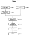
- Fig. 7 shows the flow of manufacture of a microdevice (a semiconductor chip such as an IC or LSI, a liquid crystal panel, a CCD, a thin film magnetic head, a micromachine, or the like).
- a semiconductor device circuit is designed.
- step 2 form exposure control data
- the exposure control data of the exposure apparatus is formed on the basis of the designed circuit pattern.
- step 3 manufactured by using a material such as silicon.
- step 4 wafer process
- a pre-process an actual circuit is formed on the wafer by lithography using the exposure apparatus, to which the prepared exposure control data has been input, and the wafer.
- step 5 assembly
- step 6 inspection
- step 7 inspections such as the operation confirmation test and durability test of the semiconductor device manufactured in step 5 are conducted. After these steps, the semiconductor device is completed, and shipped (step 7).
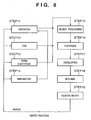
- Fig. 8 shows the detailed flow of the wafer process.
- step 11 oxidation
- step 12 CVD
- step 13 form electrode
- step 14 implant ion
- ions are implanted in the wafer.
- step 15 resist processing
- step 16 exposure
- step 18 etching
- step 19 etching
- Another application field of the present invention includes a charged particle beam applied apparatus, e.g., a length measurement apparatus for measuring the size of a pattern formed on a semiconductor substrate by using a plurality of charged particle beams generated by the arrangement as shown in Fig. 2 , a microscope apparatus for observing the pattern state, or an inspection apparatus for inspecting a pattern defect.
- a charged particle beam applied apparatus e.g., a length measurement apparatus for measuring the size of a pattern formed on a semiconductor substrate by using a plurality of charged particle beams generated by the arrangement as shown in Fig. 2 , a microscope apparatus for observing the pattern state, or an inspection apparatus for inspecting a pattern defect.
- a charged particle beam drawing apparatus that can draw a micropattern without increasing the performance of, e.g., a reduction electron optical system, can be provided. If a device is manufactured by using this apparatus, a device with higher precision than that with the prior art can be manufactured.
- length measurement, observation, and inspection can be performed within a short period of time with the plurality of generated charged particle beams.
Description
- The present invention relates to a charged particle beam exposure apparatus, a device manufacturing method, and, more particularly, to a charged particle beam exposure apparatus for drawing a pattern on a substrate by using a plurality of charged particle beams, and a device manufacturing method using the same
- An example of an electron beam exposure apparatus includes, e.g., a point beam type apparatus which uses an electron beam formed into a spot, a variable shaped beam type apparatus which uses an electron beam formed into a variable-size rectangle, and a stencil mask type apparatus with which a stencil mask having a beam passing hole with a desired shape is formed in advance and which uses a beam formed into a desired shape with the stencil.
- Although the point beam type apparatus is suitable for forming a micropattern, it is used only for research and development as its throughput is very low. The variable shaped beam type apparatus has a throughput higher than that of the point beam type apparatus by one or two orders of magnitude. This throughput, however, is still low to draw a pattern in which micropatterns of about 100 nm are packed at a high integration degree.
- An example of a method that can draw any pattern includes an exposure method using a two-dimensional blanking aperture array (e.g., see
Japanese Utility Model Publication No. 56-19402 -
Fig. 9 schematically shows the arrangement of the two-dimensional blanking aperture array. In the two-dimensional blanking aperture array, a plurality of apertures (AP) are two-dimensionally arranged, and each aperture has a pair of electrodes (EL). The two-dimensional blanking array aperture has wiring lines and elements for individually controlling voltages to be applied to the electrodes of the plurality of apertures in accordance with pattern data. For example, the apertures (AP) have diameters of 20 µm and are arranged with pitches of 100 µm. Each electrode (EL) has a thickness of 10 µm, a width of 10 µm, and a length (in the direction of depth) of about 50 µm. - In general, when the surface of a sample is scanned with an electron beam to draw a pattern with a line width of 100 nm, the spot size of the electron beam on the spot must be 25 nm or less.
- Currently, however, the sizes of the apertures of the blanker array are limited to 10 µm x 10 µm at minimum due to limitations in the manufacture. To reduce the spot size of the electron beam, the shape of which is defined by such an aperture, with a reduction electron optical system to 25 nm or less, the reduction electron optical system must have a reduction magnification of 400 times, which is actually difficult to achieve.
- Document
US-A-6 104 035 discloses an electron-beam exposure apparatus and method. The multi electron-beam exposure apparatus deflects a plurality of electron beams on an exposed surface, and upon each deflection, respectively controls irradiation of the respective electron beams. The apparatus writes a pattern by sequentially writing pattern parts of the pattern on subfields each composed of a plurality of elementary exposure fields, by simultaneously writing patterns on the respective elementary exposure fields. Pattern data of the pattern written on the exposed surface is divided in units of subfields, and as a control method for exposure of each subfield, a first control method to deflect the plurality of electron beams by a predetermined deflection width and set the electron beams, or a second control method to deflect the plurality of electron beams without setting the electron beams at positions where all the electron beams are cut off, is selected based on the divided pattern data for the subfield. - Document
US-A-5 973 332 discloses an electron beam exposure method, and a device manufacturing method using same. A corresponding electron beam exposure apparatus having a source for emitting an electron beam and a reduction electron optical system for reducing and projecting, on a target exposure surface, an image of the source, includes a correction electron optical system which is arranged between the source and the reduction electron optical system to form a plurality of intermediate images of the source along a direction perpendicular to the optical axis of the reduction electron optical system, and corrects in advance aberrations generated when the intermediate images are reduced and projected on the target exposure surface by the reduction electron optical system - The present invention has been made in view of the above situation, and one of its objects is to realize micropattern drawing without increasing the performance of a reduction electron optical system.
- It is another object of the present invention to obtain a plurality of controllable very thin charged particle beams without increasing the performance of the reduction electron optical system.
- These objects are achieved by a charged particle beam exposure apparatus according to
claim 1 and a device manufacturing method according toclaim 5. - Advantageous further developments are as set forth in the respective dependent claims.
- Other features and advantages of the present invention will be apparent from the following description taken in conjunction with the accompanying drawings, in which like reference characters designate the same or similar parts throughout the figures thereof.
- The accompanying drawings, which are incorporated in and constitute a part of the specification, illustrate embodiments of the invention and, together with the description, serve to explain the principles of the invention. In the drawings:
-
Fig. 1 is a view showing the schematic arrangement of an electron beam exposure apparatus according to a preferred embodiment of the present invention; -
Fig. 2 is a view for explaining the detailed arrangement of a multi-beam electronoptical system 3 shown inFig. 1 ; -
Fig. 3 is a view for explaining one deflector of a deflector array DA; -
Fig. 4 is a view for explaining a first electron optical system ALA1; -
Fig. 5 is a block diagram for explaining the system arrangement of the electron beam exposure apparatus shown inFig. 1 ; -
Fig. 6 includes views for explaining an exposure region and exposure method; -
Fig. 7 is a flow chart for explaining the manufacturing flow of a microdevice; -
Fig. 8 is a flow chart for explaining a wafer process; and -
Fig. 9 is a view for explaining a blanker array in a conventional multi-charged-particle-beam exposure apparatus. - An electron beam exposure apparatus will be shown as an example of an exposure apparatus that utilizes a charged particle beam. Note that the present invention is not limited to an exposure apparatus that uses an electron beam but can be similarly applied to, e.g., an exposure apparatus that uses an ion beam.
-
Fig. 1 is a view showing the schematic arrangement of an electron beam exposure apparatus-according to a preferred embodiment of the present invention. - This electron beam exposure apparatus adopts an
electron gun 1 as a charged particle beam source. Theelectron gun 1 is constituted by acathode 1a,grid 1b, and anode 1c. Electrons emitted from thecathode 1a form a cross-over image between thegrid 1b and anode 1c. In the following description, this cross-over image is called an electron source ES. - An electron beam emitted from the electron source ES is formed by a condenser lens
optical system 2 into a substantially parallel electron beam, which then irradiates a multi-beam formingoptical system 3. Typically, thecondenser lens 2 is comprised of an electron lens (unipotential lens) made up of three aperture electrodes. - The multi-beam forming
optical system 3 is comprised of an aperture array AA, deflector array DA, lens array LA, blanker array BA, and correction lens array CLA sequentially arranged from theelectron gun 1 side along an optical axis AX. The detailed arrangement of the multi-beam formingoptical system 3 will be described later. - The multi-beam forming
optical system 3 forms a plurality of intermediate images of the electron source ES. The respective intermediate images are reduced and projected by a reduction electron optical system 4 -(to be described later) onto a wafer (sample) 5. Hence, the images of the electron source ES are formed on thewafer 5. - The reduction electron
optical system 4 is comprised of symmetric magnetic tablets constituted by a first projection lens 41 (43) and second projection lens 42 (44). The distance between the twolenses - A
deflector 6 deflects the plurality of electron beams from the multi-beam formingoptical system 3 to displace the plurality of images of the electron source ES in the X and Y directions on thewafer 5 by substantially the same displacement amounts. Although not shown, thedeflector 6 is comprised of a main deflector used when the deflection width is large, and a subdeflector used when the deflection width is small. The main deflector is typically an electromagnetic deflector, and the subdeflector is typically an electrostatic deflector. - A
dynamic focus coil 7 corrects an error in focal position of the image of the electron source ES which is caused by deflection aberration occurs when thedeflector 6 is operated. A dynamicstigmatic coil 8 corrects astigmatism of the deflection aberration caused by deflection. - A θ-
Z stage 9 places thewafer 5 on it and moves in the direction of the optical axis AX (Z-axis) and a rotational direction about the Z-axis. Astage reference plate 10 is fixed to the θ-Z stage 9. - An
X-Y stage 11 moves the θ-Z stage 9 in X and Y directions perpendicular to the optical axis AX (Z-axis). - A reflected
electron detector 12 detects reflected electrons produced when a mark on thestage reference plate 10 is irradiated with the electron beam. - The multi-beam forming
optical system 3 mounted on the electron beam exposure apparatus shown inFig. 1 will be described with reference toFig. 2 . - As shown in
Fig. 2 , the multi-beam formingoptical system 3 is typically comprised of the aperture array AA, deflector array DA, lens array LA, blanker array BA, and correction lens array CLA. - The aperture array AA is formed of a substrate with a plurality of apertures. One electron beam which is made by the
condenser lens 2 to be almost parallel is divided into a plurality of electron beams when it passes through the plurality of apertures. - The deflector array DA is obtained by forming a plurality of deflectors, that individually deflect the plurality of electron beams divided by the aperture array AA, on one substrate. This substrate has a plurality of apertures. This substrate also has four pairs of electrodes arranged to sandwich the corresponding apertures. Namely, the apertures have eight deflection electrodes with deflecting functions. This substrate also has wiring lines for individually operating the deflection electrodes.
- The lens array LA is basically comprised of three substrates each having a plurality of aperture electrodes. One upper aperture electrode, one intermediate aperture electrode, and one lower aperture electrode form one electron lens (a so-called unipotential lens). In other words, the lens array LA has a plurality of electron lenses arrayed two-dimensionally. The same potential is applied to the upper, intermediate, and lower aperture electrodes so the plurality of electron lenses have the same optical characteristics (e.g., focal length).
- The blanker array BA is obtained by forming a plurality of deflectors that individually deflect the plurality of electron beams on one substrate.
Fig. 3 shows one of these deflectors in detail. Asubstrate 31 has apertures AP and pairs ofdeflection electrodes 32 each sandwiching the corresponding aperture AP. Thesubstrate 31 also has wiring lines (W) for individually controlling the plurality ofdeflection electrodes 32, thereby individually controlling deflection of the plurality of electron beams. - The correction lens array CLA is comprised of first and second electron lens arrays ALA1 and ALA2, each of which is an electron lens array formed by arranging a plurality of electron lenses two-dimensionally within one plane, and the stopper array SA.
-
Fig. 4 is a view for explaining the first electron optical system array ALA1. The first electron lens array ALA1 has three electrodes, i.e., upper, intermediate, and lower electrode plates UE, CE, and LE, each having a plurality of annular electrodes arranged in rows to correspond to the plurality of apertures. The three electrode plates are overlaid on each other through insulators. The annular electrodes with the same X and Y coordinates on the upper, intermediate, and lower electrode plates serve as one electron lens (a so-called unipotential lens) UL. All the annular electrodes of the upper and lower electrode plates of the respective electron lenses UL are connected to aCLA control circuit 111 through common wring lines (W), and are set at the same potential. In this example, the potentials of the upper and lower annular electrodes serve as electron beam accelerating potentials. - The annular electrodes of the intermediate electrode plates of the respective electron lenses are connected to the
CLA control circuit 111 through the individual wiring lines (W), and are set to desired potentials. Thus, the electron optical power (focal length) of each electron lens UL can be set to a desired value. The second electron lens array ALA2 has the same structure and function as those of the first electron lens array ALA1. - The stopper array SA has the same structure as that of the aperture array AA.
- The function of the multi-beam forming
optical system 3 will be described with reference toFig. 2 . The substantially parallel electron beam passing through thecondenser lens 2 is divided into a plurality of electron beams by the aperture array AA. The plurality of divided electron beams form a plurality of intermediate images of the electron source ES on the blanker array BA through the plurality of corresponding electron lenses of the lens array LA. The intermediate images depend not on the sizes of the apertures of the aperture array AA or of the apertures of the deflector array DA, but on the size of the electron source (cross-over image) ES. As the size of the electron source ES can be reduced comparatively easily, the size of the image of the electron source ES to be formed on thewafer 5 can be reduced to, e.g., 25 nm or less. Therefore, a micropattern with a line width of, e.g., 100 nm or less, can be drawn. The plurality of electron lenses of the lens array LA form the plurality of intermediate images (real images) of the electron source ES on substantially one plane (i.e., within or in the vicinity of the plane). The blanker array BA is arranged such that its deflection points are located on this plane. - The plurality of electron beams passing through the plurality of apertures of the blanker array BA become incident on the reduction electron
optical system 4 through the plurality of electron lenses of the correction lens array CLA corresponding to them. The respective electron lenses UL arranged in the correction lens array CLA form the virtual images of the plurality of intermediate images of the electron source ES formed within the plane of the blanker array BA. More specifically, the intermediate images of the electron source ES are formed at positions other than the front focal positions of the respective electron lenses UL each comprised of two lenses. The focal lengths of the two lenses that form each electron lens UL are adjusted such that the virtual images of the intermediate images (real images) are formed at positions where they cancel the curvature of field that occurs when the electron beams pass through the reduction electronoptical system 4. - The electron beams deflected by the blanker array BA are shielded by the stopper array SA formed in the correction lens array CLA and thus do not irradiate the
wafer 5. The electron beams not deflected by the blanker array BA are not shielded by the stopper array SA formed in the correction lens array CLA and thus irradiate thewafer 5. - As described above, according to this embodiment, the plurality of intermediate images (real images) are formed on substantially one plane and the blanker array BA is arranged such that its deflection points are located on this plane. Therefore, assuming that the stopper array SA does not exist, the electron beams deflected by the blanker array BA irradiate the positions on the wafer which are substantially same to the positions irradiated with the electron beams not deflected by the blanker array BA. Such a feature provides an advantage that the electron beams do not irradiate the undesirable portion on the wafer during ON/OFF-control of the election beams by the blanker array BA.
- The system arrangement of the electron beam exposure apparatus according to this embodiment will be described with reference to
Fig. 5 . ADA control circuit 110 individually controls the plurality of deflectors (deflection electrodes) that form the deflector array DA. TheCLA control circuit 111 individually controls the focal lengths of the plurality of electron lenses UL that form the correction lens array CLA. TheBA control circuit 112 individually controls ON/OFF of the plurality of blanking electrodes that form the blanker array BA. - A
D_STIG control circuit 113 controls the dynamicstigmatic coil 8 to control the astigmatism of the reduction electronoptical system 4. AD_FOCUS control circuit 114 controls thedynamic focus coil 7 to control the focus of the reduction electronoptical system 4. Adeflection control circuit 115 controls thedeflector 6. An opticalcharacteristic control circuit 116 adjusts the optical characteristics (magnification, distortion) of the reduction electronoptical system 4. A reflectedelectron detection circuit 117 calculates the amount of reflected electrons from a signal sent from the reflectedelectron detector 12. - A stage
drive control circuit 118 drive-controls the θ-Z stage 9 and, in cooperation with a laser interferometer LIM that detects the position of theX-Y stage 11, theX-Y stage 11. - A
control system 120 reads out exposure control data from amemory 121 which stores it (e.g., including drawing pattern data), and controls the plurality of control circuits described above on the basis of the exposure control data. Thecontrol system 120 is controlled by a CPU 123 which controls the entire electron beam exposure apparatus through aninterface 122. - The exposure operation of the electron beam exposure apparatus according to this embodiment will be described with reference to
Fig. 6 . - On the basis of the exposure control data from the
memory 121, thecontrol system 120 instructs thedeflection control circuit 115 to deflect the plurality of electron beams with thedeflector 6. Thecontrol system 120 also instructs theBA control circuit 112 to turn on/off the plurality of blanking electrodes of the blanker array BA individually in accordance with a pattern (drawing pattern data) to be drawn on thewafer 5. At this time, theX-Y stage 11 continuously moves in the Y direction. The plurality of electron beams are deflected by thedeflector 6 to follow the movement of theX-Y stage 11. The electron beams scan and expose the corresponding element exposure regions (EF) on thewafer 5, as shown inFig. 6 . The element exposure regions (EF) of the respective electron beams are adjacent to each other two-dimensionally. Consequently, a subfield (SF) constituted by the plurality of element exposure regions (EF) which are set to be exposed simultaneously is exposed simultaneously. - After one subfield (SF1) is exposed, the
control system 120 instructs thedeflection control circuit 115 to deflect the plurality of electron beams by thedeflector 6 in a direction (X direction) perpendicular to the stage scanning direction (Y direction), so that the next subfield (SF2) is exposed. At this time, since the subfields are switched by deflection, the aberration with which the respective electron beams are reduced and projected through the reduction electronoptical system 4 also changes. Hence, thecontrol system 120 instructs theBA control circuit 112,D_STIG control circuit 113, andD_FOCUS control circuit 114 to adjust the blanker array BA, dynamicstigmatic coil 8, anddynamic focus coil 7 so as to correct the changed aberration. Thereafter, as described above, the respective electron beams expose the corresponding element exposure regions (EF), thereby exposing the subfield 2 (SF2). As shown inFig. 6 , subfields (SF1 to SF6) are sequentially exposed to expose a pattern onto thewafer 5. As a result, a main field (MF) constituted by the subfields (SF1 to SF6) arranged in a direction (X direction) perpendicular to the stage scanning direction (Y direction) is exposed on thewafer 5. - After a main field 1 (MF1) shown in
Fig. 6 is exposed, thecontrol system 120 instructs thedeflection control circuit 115 to sequentially deflect the plurality of electron beams toward main fields (MF2, MF3, MF4,...) arranged in the stage scanning direction (Y direction), thus exposing them. As a result, as shown inFig. 6 , a stripe (STRIPE1) constituted by the main fields (MF2, MF3, MF4,...) is exposed. Then, theX-Y stage 11 is stepped in the X direction to expose the next stripe (STRIPE2). - A device manufacturing method using the exposure apparatus according to the present invention, represented by the electron beam exposure apparatus described above, will be described.
-
Fig. 7 shows the flow of manufacture of a microdevice (a semiconductor chip such as an IC or LSI, a liquid crystal panel, a CCD, a thin film magnetic head, a micromachine, or the like). In step 1 (design circuit), a semiconductor device circuit is designed. In step 2 (form exposure control data), the exposure control data of the exposure apparatus is formed on the basis of the designed circuit pattern. In step 3 (manufacture wafer), a wafer is manufactured by using a material such as silicon. In step 4 (wafer process) called a pre-process, an actual circuit is formed on the wafer by lithography using the exposure apparatus, to which the prepared exposure control data has been input, and the wafer. In step 5 (assembly) called a post-process, a semiconductor chip is formed by using the wafer fabricated instep 4, and includes processes such as an assembly process (dicing and bonding) and packaging process (chip encapsulation). In step 6 (inspection), inspections such as the operation confirmation test and durability test of the semiconductor device manufactured instep 5 are conducted. After these steps, the semiconductor device is completed, and shipped (step 7). -
Fig. 8 shows the detailed flow of the wafer process. In step 11 (oxidation), the surface of the wafer is oxidized. In step 12 (CVD), an insulating film is formed on the wafer surface. In step 13 (form electrode), an electrode is formed on the wafer by vapor deposition. In step 14 (implant ion), ions are implanted in the wafer. In step 15 (resist processing), a photosensitive agent is applied to the wafer. In step 16 (exposure), the above-mentioned exposure apparatus exposes the circuit pattern to the wafer. In step 17 (developing), the exposed wafer is developed. In step 18 (etching), the resist is etched except for the developed resist image. In step 19 (remove resist), an unnecessary resist after etching is removed. These steps are repeated to form multiple circuit patterns on the wafer. - With the manufacturing method according to this embodiment, a highly integrated semiconductor device which is conventionally difficult to manufacture can be manufactured at a low cost.
- Another application field of the present invention includes a charged particle beam applied apparatus, e.g., a length measurement apparatus for measuring the size of a pattern formed on a semiconductor substrate by using a plurality of charged particle beams generated by the arrangement as shown in
Fig. 2 , a microscope apparatus for observing the pattern state, or an inspection apparatus for inspecting a pattern defect. - According to one aspect of the present invention, a charged particle beam drawing apparatus that can draw a micropattern without increasing the performance of, e.g., a reduction electron optical system, can be provided. If a device is manufactured by using this apparatus, a device with higher precision than that with the prior art can be manufactured.
- According to another aspect of the present invention, length measurement, observation, and inspection can be performed within a short period of time with the plurality of generated charged particle beams.
- As many apparently widely different embodiments of the present invention can be made without departing from the scope of the appended claims, it is to be understood that the invention is not limited to the specific embodiments thereof except as defined in the claims.
Claims (5)
- A charged particle beam exposure apparatus for drawing a pattern on a substrate (5) by using a plurality of charged particle beams, comprising:a charged particle source (1, ES) for emitting a charged particle beam;an electron optical element (3) for forming a plurality of intermediate images of said charged particle source (1, ES) within a plane;a blanker array (BA) arranged on the plane and having a plurality of blankers that individually control whether to shield the plurality charged particle beams respectively forming the plurality of intermediate images; anda reduction electron optical system (4) for reducing and projecting the intermediate images formed by said electron optical element (3) onto the substrate (5),characterized by comprising a correction lens array (CLA) arranged between the plane and said reduction electron optical system (4), said correction lens array (CLA) having a plurality of electron lenses (ALA1, ALA2) arranged for respectively forming virtual images of the plurality of intermediate images formed by said electron optical element (3) at positions where they cancel a curvature of field of said reduction electron optical system (4).
- The apparatus according to claim 1, wherein
the blankers arranged in said blanker array (BA) deflect a charged particle beam that should be shielded and do not deflect a charged particle beam that should not be shielded, and
said correction lens array (CLA) has a stopper array (SA) for shielding and passing therethrough, among a plurality of charged particle beams passing through the plurality of blankers arranged in said blanker array (BA), deflected and undeflected charged particle beams, respectively. - The apparatus according to claim 1, wherein
the blankers arranged in said blanker array (BA) deflect a charged particle beam that should be shielded and do not deflect a charged particle beam that should not be shielded, and
said charged particle beam exposure apparatus further comprises a stopper array (SA) for shielding and passing therethrough, among a plurality of charged particle beams passing through the plurality of blankers arranged in said blanker array (BA), deflected and undeflected charged particle beams, respectively. - The apparatus according to claim 1, wherein said electron optical element (3) has
an aperture array (AA) obtained by arranging a plurality of apertures for passing the charged particle beam emitted by said charged particle source (1, ES) therethrough, and
a lens array (LA) obtained by arranging a plurality of electron lenses for forming the plurality of intermediate images within the plane with the plurality of charged particle beams respectively passing through the plurality of apertures. - A device manufacturing method comprising the steps of:applying a photosensitive material on a substrate (5);drawing a pattern on the substrate (5) coated with the photosensitive material with a charged particle beam exposure apparatus, anddeveloping the photosensitive material on the substrate (5) drawn with the pattern,the charged particle beam exposure apparatus comprisinga charged particle source (1, ES) for emitting a charged particle beam,an electron optical element (3) for forming a plurality of intermediate images of the charged particle source (1, ES) within a plane,a blanker array (BA) arranged on the plane and having a plurality of blankers that individually control whether to shield the plurality charged particle beams respectively forming the plurality of intermediate images,a reduction electron optical system (4) for reducing and projecting the intermediate images formed by the electron optical element (3) onto the substrate (5), anda correction lens array (CLA) arranged between the plane and the reduction electron optical system (4), the correction lens array (CLA) having a plurality of electron lenses arranged for respectively forming virtual images of the plurality of intermediate images formed by the electron optical element (3) at positions where they cancel a curvature of field of the reduction electron optical system (4) .
Applications Claiming Priority (2)
| Application Number | Priority Date | Filing Date | Title |
|---|---|---|---|
| JP2001124758A JP4647820B2 (en) | 2001-04-23 | 2001-04-23 | Charged particle beam drawing apparatus and device manufacturing method |
| JP2001124758 | 2001-04-23 |
Publications (3)
| Publication Number | Publication Date |
|---|---|
| EP1253619A2 EP1253619A2 (en) | 2002-10-30 |
| EP1253619A3 EP1253619A3 (en) | 2007-11-14 |
| EP1253619B1 true EP1253619B1 (en) | 2009-10-14 |
Family
ID=18974092
Family Applications (1)
| Application Number | Title | Priority Date | Filing Date |
|---|---|---|---|
| EP02252818A Expired - Lifetime EP1253619B1 (en) | 2001-04-23 | 2002-04-22 | Charged particle beam exposure apparatus and device manufacturing method using same |
Country Status (6)
| Country | Link |
|---|---|
| US (1) | US6903353B2 (en) |
| EP (1) | EP1253619B1 (en) |
| JP (1) | JP4647820B2 (en) |
| KR (1) | KR100495651B1 (en) |
| DE (1) | DE60233994D1 (en) |
| TW (1) | TW559883B (en) |
Families Citing this family (61)
| Publication number | Priority date | Publication date | Assignee | Title |
|---|---|---|---|---|
| JP3996267B2 (en) * | 1998-05-12 | 2007-10-24 | エルピーダメモリ株式会社 | Semiconductor memory device |
| JP2001284230A (en) | 2000-03-31 | 2001-10-12 | Canon Inc | Electronic optical system array, charged particle beam exposure system provided therewith, and method of manufacturing device |
| JP4947841B2 (en) * | 2000-03-31 | 2012-06-06 | キヤノン株式会社 | Charged particle beam exposure system |
| JP4585661B2 (en) * | 2000-03-31 | 2010-11-24 | キヤノン株式会社 | Electro-optical array, charged particle beam exposure apparatus, and device manufacturing method |
| JP2001283756A (en) * | 2000-03-31 | 2001-10-12 | Canon Inc | Electron optical system array, charged particle beam exposure device using it and device manufacturing method |
| JP4947842B2 (en) * | 2000-03-31 | 2012-06-06 | キヤノン株式会社 | Charged particle beam exposure system |
| US6768125B2 (en) | 2002-01-17 | 2004-07-27 | Ims Nanofabrication, Gmbh | Maskless particle-beam system for exposing a pattern on a substrate |
| US6953938B2 (en) * | 2002-10-03 | 2005-10-11 | Canon Kabushiki Kaisha | Deflector, method of manufacturing deflector, and charged particle beam exposure apparatus |
| US7098468B2 (en) * | 2002-11-07 | 2006-08-29 | Applied Materials, Inc. | Raster frame beam system for electron beam lithography |
| EP2293316B1 (en) * | 2003-02-14 | 2012-04-04 | Mapper Lithography IP B.V. | Dispenser cathode |
| JP4421836B2 (en) * | 2003-03-28 | 2010-02-24 | キヤノン株式会社 | Exposure apparatus and device manufacturing method |
| EP1627412B1 (en) | 2003-05-28 | 2007-04-04 | Mapper Lithography Ip B.V. | Charged particle beamlet exposure system |
| JP4738723B2 (en) * | 2003-08-06 | 2011-08-03 | キヤノン株式会社 | Multi charged particle beam drawing apparatus, charged particle beam current measuring method and device manufacturing method |
| JP4794444B2 (en) * | 2003-09-05 | 2011-10-19 | カール・ツァイス・エスエムティー・ゲーエムベーハー | Particle optical system and apparatus, and particle optical component for such system and apparatus |
| JP4313145B2 (en) | 2003-10-07 | 2009-08-12 | 株式会社日立ハイテクノロジーズ | Charged particle beam drawing method and charged particle beam drawing apparatus |
| DE10351059B4 (en) * | 2003-10-31 | 2007-03-01 | Roth & Rau Ag | Method and apparatus for ion beam machining of surfaces |
| GB2414111B (en) * | 2004-04-30 | 2010-01-27 | Ims Nanofabrication Gmbh | Advanced pattern definition for particle-beam processing |
| JP4477436B2 (en) * | 2004-06-30 | 2010-06-09 | キヤノン株式会社 | Charged particle beam exposure system |
| JP4634076B2 (en) * | 2004-06-30 | 2011-02-16 | キヤノン株式会社 | Charged particle beam exposure apparatus and device manufacturing method |
| DE102004052995A1 (en) * | 2004-11-03 | 2006-05-11 | Leica Microsystems Lithography Gmbh | Device for structuring a particle beam |
| JP4657740B2 (en) * | 2005-01-26 | 2011-03-23 | キヤノン株式会社 | Aberration measuring apparatus for charged particle beam optical system, charged particle beam exposure apparatus including the aberration measuring apparatus, and device manufacturing method using the apparatus |
| EP1851784B8 (en) * | 2005-02-11 | 2016-10-19 | IMS Nanofabrication AG | Charged-particle exposure apparatus with electrostatic zone plate |
| JP4171479B2 (en) | 2005-06-28 | 2008-10-22 | 株式会社日立ハイテクノロジーズ | Charged particle beam application apparatus and charged particle beam application method |
| JP5222142B2 (en) * | 2005-09-06 | 2013-06-26 | カール・ツァイス・エスエムティー・ゲーエムベーハー | Particle optics |
| US8134135B2 (en) * | 2006-07-25 | 2012-03-13 | Mapper Lithography Ip B.V. | Multiple beam charged particle optical system |
| WO2008013442A1 (en) * | 2006-07-25 | 2008-01-31 | Mapper Lithography Ip B.V. | A multiple beam charged particle optical system |
| EP2019415B1 (en) * | 2007-07-24 | 2016-05-11 | IMS Nanofabrication AG | Multi-beam source |
| EP2260499B1 (en) * | 2008-02-26 | 2016-11-30 | Mapper Lithography IP B.V. | Projection lens arrangement |
| JP5486163B2 (en) | 2008-03-19 | 2014-05-07 | 株式会社ニューフレアテクノロジー | Drawing system and parameter monitoring method for drawing apparatus |
| KR20110030466A (en) * | 2008-05-23 | 2011-03-23 | 마퍼 리쏘그라피 아이피 비.브이. | Imaging system |
| JP5634052B2 (en) | 2009-01-09 | 2014-12-03 | キヤノン株式会社 | Charged particle beam drawing apparatus and device manufacturing method |
| KR101714005B1 (en) | 2010-07-13 | 2017-03-09 | 삼성전자 주식회사 | Optical device and exposure apparatus including the same |
| JP5463429B2 (en) * | 2013-05-08 | 2014-04-09 | 株式会社ニューフレアテクノロジー | Charged particle drawing system and parameter monitoring method for charged particle drawing apparatus |
| JP6779788B2 (en) * | 2014-06-13 | 2020-11-04 | インテル・コーポレーション | Real-time alignment methods, columns, computer programs and computer-readable storage media |
| JP6553973B2 (en) * | 2014-09-01 | 2019-07-31 | 株式会社ニューフレアテクノロジー | Blanking apparatus for multi-charged particle beam and multi-charged particle beam drawing apparatus |
| DE102015202172B4 (en) | 2015-02-06 | 2017-01-19 | Carl Zeiss Microscopy Gmbh | Particle beam system and method for particle-optical examination of an object |
| IL256895B (en) | 2015-07-22 | 2022-08-01 | Hermes Microvision Inc | Apparatus of plural charged-particle beams |
| US11302511B2 (en) * | 2016-02-04 | 2022-04-12 | Kla Corporation | Field curvature correction for multi-beam inspection systems |
| US10418324B2 (en) | 2016-10-27 | 2019-09-17 | Asml Netherlands B.V. | Fabricating unique chips using a charged particle multi-beamlet lithography system |
| WO2018117275A1 (en) * | 2016-12-23 | 2018-06-28 | Mapper Lithography Ip B.V. | Fabricating unique chips using a charged particle multi-beamlet lithography system |
| US11062874B2 (en) * | 2016-12-30 | 2021-07-13 | Asml Netherlands B.V. | Apparatus using multiple charged particle beams |
| US10242839B2 (en) * | 2017-05-05 | 2019-03-26 | Kla-Tencor Corporation | Reduced Coulomb interactions in a multi-beam column |
| TWI742223B (en) * | 2017-01-14 | 2021-10-11 | 美商克萊譚克公司 | Electron beam system and method, and scanning electron microscope |
| US10347460B2 (en) * | 2017-03-01 | 2019-07-09 | Dongfang Jingyuan Electron Limited | Patterned substrate imaging using multiple electron beams |
| US10176965B1 (en) * | 2017-07-05 | 2019-01-08 | ICT Integrated Circuit Testing Gesellschaft für Halbleiterprüftechnik mbH | Aberration-corrected multibeam source, charged particle beam device and method of imaging or illuminating a specimen with an array of primary charged particle beamlets |
| US11670477B2 (en) | 2017-10-02 | 2023-06-06 | Asml Netherlands B.V. | Apparatus using charged particle beams |
| JP6977528B2 (en) | 2017-12-14 | 2021-12-08 | 株式会社ニューフレアテクノロジー | Aperture set for multi-beam |
| DE102018202428B3 (en) | 2018-02-16 | 2019-05-09 | Carl Zeiss Microscopy Gmbh | Multibeam Teilchenmikroskop |
| DE102018202421B3 (en) | 2018-02-16 | 2019-07-11 | Carl Zeiss Microscopy Gmbh | Multibeam particle beam |
| CN112055886A (en) | 2018-02-27 | 2020-12-08 | 卡尔蔡司MultiSEM有限责任公司 | Charged particle multi-beam system and method |
| US10811215B2 (en) | 2018-05-21 | 2020-10-20 | Carl Zeiss Multisem Gmbh | Charged particle beam system |
| DE102018007455B4 (en) | 2018-09-21 | 2020-07-09 | Carl Zeiss Multisem Gmbh | Process for detector alignment when imaging objects using a multi-beam particle microscope, system and computer program product |
| DE102018007652B4 (en) | 2018-09-27 | 2021-03-25 | Carl Zeiss Multisem Gmbh | Particle beam system and method for current regulation of single particle beams |
| DE102018124044B3 (en) | 2018-09-28 | 2020-02-06 | Carl Zeiss Microscopy Gmbh | Method for operating a multi-beam particle beam microscope and multi-beam particle beam system |
| US11145485B2 (en) * | 2018-12-26 | 2021-10-12 | Nuflare Technology, Inc. | Multiple electron beams irradiation apparatus |
| SG11202106369RA (en) * | 2018-12-31 | 2021-07-29 | Asml Netherlands Bv | Multi-beam inspection apparatus |
| CN111477530B (en) | 2019-01-24 | 2023-05-05 | 卡尔蔡司MultiSEM有限责任公司 | Method for imaging 3D samples using a multi-beam particle microscope |
| TWI743626B (en) | 2019-01-24 | 2021-10-21 | 德商卡爾蔡司多重掃描電子顯微鏡有限公司 | System comprising a multi-beam particle microscope, method for imaging a 3d sample layer by layer and computer program product |
| JP6954943B2 (en) * | 2019-03-15 | 2021-10-27 | 日本電子株式会社 | Charged particle beam device |
| EP4088301A1 (en) | 2020-01-06 | 2022-11-16 | ASML Netherlands B.V. | Charged particle assessment tool, inspection method |
| JP7409946B2 (en) * | 2020-04-13 | 2024-01-09 | 株式会社ニューフレアテクノロジー | Multi-charged particle beam irradiation equipment and multi-charged particle beam inspection equipment |
Family Cites Families (24)
| Publication number | Priority date | Publication date | Assignee | Title |
|---|---|---|---|---|
| SE421832B (en) | 1979-04-18 | 1982-02-01 | Pharos Ab | DEVICE FOR REGISTERING THE TOPOGRAPHY OF THE CHARGED MASS IN A MACHINE |
| JPH01295419A (en) * | 1988-05-24 | 1989-11-29 | Fujitsu Ltd | Method and apparatus for electron beam lithography |
| US5830612A (en) * | 1996-01-24 | 1998-11-03 | Fujitsu Limited | Method of detecting a deficiency in a charged-particle-beam exposure mask |
| EP1369897A3 (en) * | 1996-03-04 | 2005-01-19 | Canon Kabushiki Kaisha | Electron beam exposure apparatus and method, and device manufacturing method |
| JP3647128B2 (en) * | 1996-03-04 | 2005-05-11 | キヤノン株式会社 | Electron beam exposure apparatus and exposure method thereof |
| JPH09320960A (en) * | 1996-03-25 | 1997-12-12 | Nikon Corp | Charged particle beam transcription apparatus |
| JP3796317B2 (en) | 1996-06-12 | 2006-07-12 | キヤノン株式会社 | Electron beam exposure method and device manufacturing method using the same |
| US5929454A (en) | 1996-06-12 | 1999-07-27 | Canon Kabushiki Kaisha | Position detection apparatus, electron beam exposure apparatus, and methods associated with them |
| JP3728015B2 (en) | 1996-06-12 | 2005-12-21 | キヤノン株式会社 | Electron beam exposure system and device manufacturing method using the same |
| JP3927620B2 (en) | 1996-06-12 | 2007-06-13 | キヤノン株式会社 | Electron beam exposure method and device manufacturing method using the same |
| US5981954A (en) | 1997-01-16 | 1999-11-09 | Canon Kabushiki Kaisha | Electron beam exposure apparatus |
| JP3689516B2 (en) | 1997-01-29 | 2005-08-31 | キヤノン株式会社 | Electron beam exposure system |
| JPH10214779A (en) | 1997-01-31 | 1998-08-11 | Canon Inc | Electron beam exposure method and fabrication of device using that method |
| US6107636A (en) | 1997-02-07 | 2000-08-22 | Canon Kabushiki Kaisha | Electron beam exposure apparatus and its control method |
| JPH10335223A (en) * | 1997-06-02 | 1998-12-18 | Canon Inc | Electron beam exposure method and system |
| US6104035A (en) | 1997-06-02 | 2000-08-15 | Canon Kabushiki Kaisha | Electron-beam exposure apparatus and method |
| JP3787417B2 (en) | 1997-06-11 | 2006-06-21 | キヤノン株式会社 | Electron beam exposure method and electron beam exposure apparatus |
| JPH11195590A (en) * | 1998-01-05 | 1999-07-21 | Canon Inc | Multiple electron beam exposure method and its apparatus, and manufacture of device |
| US6157039A (en) * | 1998-05-07 | 2000-12-05 | Etec Systems, Inc. | Charged particle beam illumination of blanking aperture array |
| JP2000049071A (en) | 1998-07-28 | 2000-02-18 | Canon Inc | Electron beam exposure system and method therefor, and manufacture of devices |
| JP2000093825A (en) | 1998-09-21 | 2000-04-04 | Oomiya Seisakusho:Kk | Chaff pulverizer |
| JP2000251827A (en) * | 1999-03-03 | 2000-09-14 | Nikon Corp | Illumination optical system |
| JP3859404B2 (en) * | 1999-09-27 | 2006-12-20 | 株式会社東芝 | Charged beam drawing apparatus, pattern drawing method, and recording medium |
| US6566664B2 (en) * | 2000-03-17 | 2003-05-20 | Canon Kabushiki Kaisha | Charged-particle beam exposure apparatus and device manufacturing method |
-
2001
- 2001-04-23 JP JP2001124758A patent/JP4647820B2/en not_active Expired - Fee Related
-
2002
- 2002-04-19 US US10/125,439 patent/US6903353B2/en not_active Expired - Lifetime
- 2002-04-22 TW TW091108248A patent/TW559883B/en not_active IP Right Cessation
- 2002-04-22 KR KR10-2002-0021943A patent/KR100495651B1/en not_active IP Right Cessation
- 2002-04-22 EP EP02252818A patent/EP1253619B1/en not_active Expired - Lifetime
- 2002-04-22 DE DE60233994T patent/DE60233994D1/en not_active Expired - Lifetime
Also Published As
| Publication number | Publication date |
|---|---|
| EP1253619A3 (en) | 2007-11-14 |
| US20020160311A1 (en) | 2002-10-31 |
| KR20020082769A (en) | 2002-10-31 |
| TW559883B (en) | 2003-11-01 |
| EP1253619A2 (en) | 2002-10-30 |
| JP2002319532A (en) | 2002-10-31 |
| JP4647820B2 (en) | 2011-03-09 |
| KR100495651B1 (en) | 2005-06-16 |
| US6903353B2 (en) | 2005-06-07 |
| DE60233994D1 (en) | 2009-11-26 |
Similar Documents
| Publication | Publication Date | Title |
|---|---|---|
| EP1253619B1 (en) | Charged particle beam exposure apparatus and device manufacturing method using same | |
| US6472672B1 (en) | Electron beam exposure apparatus and its control method | |
| US7005658B2 (en) | Charged particle beam exposure apparatus and method | |
| EP0794552B1 (en) | Electron beam exposure apparatus and method, and device manufacturing method | |
| US6137113A (en) | Electron beam exposure method and apparatus | |
| US6515409B2 (en) | Charged-particle beam exposure apparatus, exposure system, control method therefor, and device manufacturing method | |
| US6552353B1 (en) | Multi-electron beam exposure method and apparatus and device manufacturing method | |
| JPH1064812A (en) | Electronic beam exposure method and device manufacturing method using it | |
| US6903352B2 (en) | Charged-particle beam exposure apparatus, charged-particle beam exposure method, control data determination method, and device manufacturing method using this method | |
| US6657210B1 (en) | Electron beam exposure method, a method of constructing exposure control data, and a computer-readable medium | |
| JPH1187206A (en) | Electron beam aligner and manufacture of device using the same | |
| JP5159035B2 (en) | Lens array and charged particle beam exposure apparatus including the lens array | |
| US7049610B2 (en) | Charged particle beam exposure method, charged particle beam exposure apparatus, and device manufacturing method | |
| JP4018197B2 (en) | Electron beam exposure method and electron beam exposure apparatus | |
| US7005659B2 (en) | Charged particle beam exposure apparatus, charged particle beam exposure method, and device manufacturing method using the same apparatus | |
| JP3647143B2 (en) | Electron beam exposure apparatus and exposure method therefor | |
| JP4143204B2 (en) | Charged particle beam exposure apparatus and device manufacturing method using the apparatus | |
| JP3728315B2 (en) | Electron beam exposure apparatus, electron beam exposure method, and device manufacturing method | |
| JP4006054B2 (en) | Electron beam exposure system | |
| JPH10321509A (en) | Method and device for electron beam exposure | |
| JP2007329221A (en) | Charged particle beam lens array, photolithographic apparatus, and device manufacturing method | |
| JPH09330868A (en) | Electron beam exposure method and manufacture of device using it | |
| JPH10214778A (en) | Electron beam aligner and alleging method | |
| JPH10321508A (en) | Method and device for electron beam exposure |
Legal Events
| Date | Code | Title | Description |
|---|---|---|---|
| PUAI | Public reference made under article 153(3) epc to a published international application that has entered the european phase |
Free format text: ORIGINAL CODE: 0009012 |
|
| AK | Designated contracting states |
Kind code of ref document: A2 Designated state(s): AT BE CH CY DE DK ES FI FR GB GR IE IT LI LU MC NL PT SE TR |
|
| AX | Request for extension of the european patent |
Free format text: AL;LT;LV;MK;RO;SI |
|
| PUAL | Search report despatched |
Free format text: ORIGINAL CODE: 0009013 |
|
| AK | Designated contracting states |
Kind code of ref document: A3 Designated state(s): AT BE CH CY DE DK ES FI FR GB GR IE IT LI LU MC NL PT SE TR |
|
| AX | Request for extension of the european patent |
Extension state: AL LT LV MK RO SI |
|
| 17P | Request for examination filed |
Effective date: 20080328 |
|
| 17Q | First examination report despatched |
Effective date: 20080513 |
|
| AKX | Designation fees paid |
Designated state(s): DE GB NL |
|
| GRAP | Despatch of communication of intention to grant a patent |
Free format text: ORIGINAL CODE: EPIDOSNIGR1 |
|
| GRAS | Grant fee paid |
Free format text: ORIGINAL CODE: EPIDOSNIGR3 |
|
| GRAA | (expected) grant |
Free format text: ORIGINAL CODE: 0009210 |
|
| RIN1 | Information on inventor provided before grant (corrected) |
Inventor name: HASHIMOTO, SHINICHI Inventor name: SOHDA, YASUNARI, HITACHI, LTD., I.P.G Inventor name: MURAKI, MASATO |
|
| AK | Designated contracting states |
Kind code of ref document: B1 Designated state(s): DE GB NL |
|
| REG | Reference to a national code |
Ref country code: GB Ref legal event code: FG4D |
|
| REF | Corresponds to: |
Ref document number: 60233994 Country of ref document: DE Date of ref document: 20091126 Kind code of ref document: P |
|
| PLBE | No opposition filed within time limit |
Free format text: ORIGINAL CODE: 0009261 |
|
| STAA | Information on the status of an ep patent application or granted ep patent |
Free format text: STATUS: NO OPPOSITION FILED WITHIN TIME LIMIT |
|
| 26N | No opposition filed |
Effective date: 20100715 |
|
| GBPC | Gb: european patent ceased through non-payment of renewal fee |
Effective date: 20100422 |
|
| PG25 | Lapsed in a contracting state [announced via postgrant information from national office to epo] |
Ref country code: GB Free format text: LAPSE BECAUSE OF NON-PAYMENT OF DUE FEES Effective date: 20100422 |
|
| PGFP | Annual fee paid to national office [announced via postgrant information from national office to epo] |
Ref country code: NL Payment date: 20130416 Year of fee payment: 12 |
|
| REG | Reference to a national code |
Ref country code: NL Ref legal event code: V1 Effective date: 20141101 |
|
| PG25 | Lapsed in a contracting state [announced via postgrant information from national office to epo] |
Ref country code: NL Free format text: LAPSE BECAUSE OF NON-PAYMENT OF DUE FEES Effective date: 20141101 |
|
| REG | Reference to a national code |
Ref country code: DE Ref legal event code: R081 Ref document number: 60233994 Country of ref document: DE Owner name: ADVANTEST CORP., JP Free format text: FORMER OWNERS: CANON K.K., TOKYO, JP; HITACHI, LTD., TOKYO, JP; ADVANTEST CORP., TOKIO/TOKYO, JP Ref country code: DE Ref legal event code: R082 Ref document number: 60233994 Country of ref document: DE Representative=s name: TBK, DE |
|
| PGFP | Annual fee paid to national office [announced via postgrant information from national office to epo] |
Ref country code: DE Payment date: 20170420 Year of fee payment: 16 |
|
| REG | Reference to a national code |
Ref country code: DE Ref legal event code: R119 Ref document number: 60233994 Country of ref document: DE |
|
| PG25 | Lapsed in a contracting state [announced via postgrant information from national office to epo] |
Ref country code: DE Free format text: LAPSE BECAUSE OF NON-PAYMENT OF DUE FEES Effective date: 20181101 |