EP1243028B1 - L- and u-gate devices for soi/sos applications - Google Patents
L- and u-gate devices for soi/sos applications Download PDFInfo
- Publication number
- EP1243028B1 EP1243028B1 EP00988112A EP00988112A EP1243028B1 EP 1243028 B1 EP1243028 B1 EP 1243028B1 EP 00988112 A EP00988112 A EP 00988112A EP 00988112 A EP00988112 A EP 00988112A EP 1243028 B1 EP1243028 B1 EP 1243028B1
- Authority
- EP
- European Patent Office
- Prior art keywords
- leg
- region
- shaped gate
- gate
- active region
- Prior art date
- Legal status (The legal status is an assumption and is not a legal conclusion. Google has not performed a legal analysis and makes no representation as to the accuracy of the status listed.)
- Expired - Lifetime
Links
Images


Classifications
-
- H—ELECTRICITY
- H10—SEMICONDUCTOR DEVICES; ELECTRIC SOLID-STATE DEVICES NOT OTHERWISE PROVIDED FOR
- H10D—INORGANIC ELECTRIC SEMICONDUCTOR DEVICES
- H10D30/00—Field-effect transistors [FET]
- H10D30/60—Insulated-gate field-effect transistors [IGFET]
- H10D30/67—Thin-film transistors [TFT]
- H10D30/6704—Thin-film transistors [TFT] having supplementary regions or layers in the thin films or in the insulated bulk substrates for controlling properties of the device
- H10D30/6708—Thin-film transistors [TFT] having supplementary regions or layers in the thin films or in the insulated bulk substrates for controlling properties of the device for preventing the kink effect or the snapback effect, e.g. discharging the minority carriers of the channel region for preventing bipolar effect
- H10D30/6711—Thin-film transistors [TFT] having supplementary regions or layers in the thin films or in the insulated bulk substrates for controlling properties of the device for preventing the kink effect or the snapback effect, e.g. discharging the minority carriers of the channel region for preventing bipolar effect by using electrodes contacting the supplementary regions or layers
-
- H—ELECTRICITY
- H10—SEMICONDUCTOR DEVICES; ELECTRIC SOLID-STATE DEVICES NOT OTHERWISE PROVIDED FOR
- H10D—INORGANIC ELECTRIC SEMICONDUCTOR DEVICES
- H10D30/00—Field-effect transistors [FET]
- H10D30/60—Insulated-gate field-effect transistors [IGFET]
- H10D30/67—Thin-film transistors [TFT]
- H10D30/6729—Thin-film transistors [TFT] characterised by the electrodes
- H10D30/673—Thin-film transistors [TFT] characterised by the electrodes characterised by the shapes, relative sizes or dispositions of the gate electrodes
- H10D30/6733—Multi-gate TFTs
-
- H—ELECTRICITY
- H10—SEMICONDUCTOR DEVICES; ELECTRIC SOLID-STATE DEVICES NOT OTHERWISE PROVIDED FOR
- H10D—INORGANIC ELECTRIC SEMICONDUCTOR DEVICES
- H10D86/00—Integrated devices formed in or on insulating or conducting substrates, e.g. formed in silicon-on-insulator [SOI] substrates or on stainless steel or glass substrates
- H10D86/201—Integrated devices formed in or on insulating or conducting substrates, e.g. formed in silicon-on-insulator [SOI] substrates or on stainless steel or glass substrates the substrates comprising an insulating layer on a semiconductor body, e.g. SOI
Definitions
- the present invention relates to semiconductor devices, and more particularly to semiconductor devices that are formed in a thin film of semiconductor material that sits atop an insulating layer, such as Silicon-on-Insulator (SOI) or Silicon-on-Sapphire (SOS) semiconductor devices.
- SOI Silicon-on-Insulator
- SOS Silicon-on-Sapphire
- Thin film, co-planar integrated circuits employing silicon-on-insulator (SOI) or silicon-on-sapphire (SOS) CMOS technology typically include a semiconductor (silicon) layer, which is disposed atop a substrate-supported dielectric (silicon dioxide) layer, with the side wall perimeter of the devices bounded by an air or (oxide) dielectric layer.
- SOI silicon-on-insulator
- SOS silicon-on-sapphire
- CMOS silicon-on-sapphire
- This semiconductor structure typically includes a body/channel region disposed between and immediately contiguous with respective source and drain regions.
- a doped polysilicon gate layer Overlying the channel/body region and extending onto the surrounding support substrate is a doped polysilicon gate layer, which is insulated from the semiconductor material by a thin dielectric layer (e.g., gate oxide).
- the air or oxide dielectric layer that bounds the side wall perimeter of the device typically extends under the polysilicon gate layer and forms the side wall of the channel/body region.
- a silicide layer is often provided over the polysilicon gate, and over the source and drain regions.
- a disadvantage of many SOI transistors is the lack of a bulk silicon or body contact to the MOS transistor. If the channel/body region is left “floating", various hysteresis effects can prevent proper circuit operation. These effects include the so-called “kink” effect and the parasitic lateral bipolar action.
- the "kink” effect originates from impact ionization. For example, when an N-channel SOI/SOS MOSFET operates at a relatively large drain-to-source voltage, channel electrons with sufficient energy cause impact ionization near the drain end of the channel. The generated holes build up in the channel/body region of the device, thereby raising the body potential. The increased body potential reduces the threshold voltage of the MOSFET, which increases the MOSFET current and causes the so-called "kink” in the MOSFET current vs. voltage (I-V) curves.
- the body bias may be raised sufficiently so that the source to body p-n junction is forward biased.
- the resulting emission of minority carriers into the channel/body region may cause a parasitic NPN bipolar transistor between the source, body and drain to turn on, leading to loss of gate control over the MOSFET current.
- Both the "kink” effect and the parasitic bipolar effect can be avoided if charge is not allowed to accumulate in the channel/body region.
- a body contact is often used to extract the charge collected in the body/channel region. Because the hole charge in the channel/body region will move to lower potential regions, the body contact and the source terminals can be tied together to eliminate the "floating body” effects.
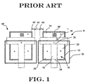
- FIG. 1 shows a typical prior art N-channel SOI MOSFET with body control.
- the MOSFET is generally shown at 8, and is commonly called a T-gate MOSFET because of the T-shape of gate 14.
- the T-gate MOSFET 8 has an active region 10 formed on an insulating layer and surrounded by an isolation region 12.
- the active region 10 is divided into three regions by T-gate 14, including the source region 20, the drain region 22 and the body-tie region 24.
- the T-gate 14 includes a first leg 16 and a second leg 18.
- the N-type source/drain regions 20 and 22 are located on either side of the first leg 16 and along the lower side of the second leg 18.
- a P-type body tie region 24 is located above the second leg 18. Located under the first and second legs 16 and 18 is a p-type body/channel region.
- the active region 10 and isolation region 12 are provided using known techniques.
- a thin gate oxide layer is provided over the active region 10, followed by a doped polysilicon gate layer.
- the doped polysilicon gate layer and the gate oxide layer are selectively etched to form the T-shaped gate 14.
- the source and drain regions 20 and 22 are then selectively doped with an N-type dopant (for an N-channel device).
- a mask, such as mask 30, is used to define the area that is to be exposed to the N-type dopant.
- the body tie region 24 is selectively doped with a P-type dopant.
- the source region 20, the drain region 22, the body tie region 24, and the gate 14 are each covered with a silicide layer to reduce the resistance thereof.
- the T-gate configuration has a number of advantageous.
- the T-gate configuration provides a body tie connection to the body/channel region under gate 14.
- holes that are generated in the body/channel region under the first leg 16 of gate 14 pass through the P-type region under the second leg 18, and arrive at the P-type body tie region 24 where they are collected by the body tie contact 26.
- the T-gate configuration may reduce or eliminate the substrate floating effects discussed above.
- the second leg 18 eliminates the channel/dielectric interface along the upper side wall 32 of the body/channel region under the first leg 16. Accordingly, the chance that a parasitic channel will be formed along the upper side wall 32 due to ionizing radiation is reduced or eliminated.
- the second leg 18 also functions to prevent the silicide layer from connecting the body tie region 24 and the source region 20 and drain region 22.
- T-gate configuration A limitation of the T-gate configuration is that the channel/dielectric interface along the lower side wall 34 of the channel remains. Thus, there is still a danger that a leakage path or "parasitic" channel may be induced along the lower side wall 34 when exposed to ionizing radiation. As indicated above, this can result in significant current leakage when the device is turned off.
- T-gate configuration Another limitation of the T-gate configuration is that a separate body tie region 24 and body tie contact 26 must be provided. Most manufacturing processes have minimum spacing requirements including poly-to-contact and contact-to-field spacings. These minimum spacing requirements often result in a substantial distance between the second leg 18 and the upper edge of the active region 10, thereby reducing the packing density that can be achieved for the device. Finally, one or more metal routes must typically be provided to the body tie contact 26. These metal routes may further reduce the packing density that can be achieved by increasing congestion on the metal layer.
- T-gate configuration Another limitation of the T-gate configuration is that the lateral pitch for two adjacent transistors must typically be relatively large. To illustrate this, a second T-gate transistor is shown at 48. Because the second leg 18 must extend beyond both the left and right edges of the active region 10, each transistor must be provided in a separate active region. This alone reduces the packing density that can be achieved for the device. In addition, however, most manufacturing processes have minimum spacing requirements including poly-enclosure-of-field 40 and poly-to-poly spacing 42. These minimum spacing requirements can also significantly increase the minimum lateral pitch of two adjacent T-gate transistors.
- the second leg 18 of the T-gate 14 increases the gate area of each transistor.
- the additional gate area increases the capacitance of gate 14, which reduces the speed of the device.
- the additional gate area also increases the thin gate oxide area, which can reduce the overall yield of the device.
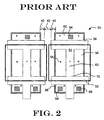
- FIG. 2 shows another prior art N-channel SOI MOSFET with body control.
- the MOSFET is generally shown at 50, and is often referred to as an H-gate MOSFET because of the H-shape of gate 51.
- the H-gate MOSFET 50 is similar to the T-gate MOSFET of Figure 1, but further includes a third leg 52 along the bottom of the source and drain regions 54 and 56.
- An advantage of the H-gate configuration is that the third leg 52 helps eliminate the channel/dielectric interface along the lower side wall 70 of the body/channel region under the first leg 60. As such, the chance that a parasitic channel will be formed along the lower side wall 70 due to ionizing radiation is reduced.
- the third leg 52 also functions to prevent the silicide layer from connecting the body tie region 66 to the source region 54 and the drain region 56.
- Holes generated in the body/channel region under first leg 60 may pass through the P-type region under the second leg 58, and arrive at the P-type body tie region 62 where they are collected by the body tie contact 64.
- the holes may also pass through the P-type region under the third leg 52, and arrive at the P-type body tie region 66, where they are collected by the body tie contacts 68. Because there are two parallel paths from the body/channel region to body tie contacts, the resistance from the body tie contacts to the body/channel region is effectively halved relative to the T-gate configuration discussed above. This allows the body/channel region to be about twice as long as the T-gate configuration of Figure 1 while affording the same level of protection.
- a limitation of the H-gate configuration is that body contacts must be provided either above the second leg 58 or below the third leg 52, or both. Since most manufacturing processes have minimum spacing requirements including poly-to-contact and contact-to-field spacings, a substantial space may be required between the second leg 58 and the upper edge of the active region or between the third leg 52 and the bottom edge of the active region, or both. Furthermore, one or more metal routes must typically be provided to the upper body contact 64 and/or the lower body contacts 68. Both of these may reduce the packing density that can be achieved.
- H-gate configuration Another limitation of the H-gate configuration is that the additional gate area of the third leg 52 increases the capacitance of the gate 51, which as described above, can reduce the speed of the device. In addition, the additional gate area of the third leg 52 increases the thin gate oxide area, which can reduce the overall yield of the device.
- US-5,317,181 generally describes a first implant region extending to the source and a conducting layer electrically connecting the first implant region to the source.
- DE 19623846 generally describes common implant regions (body ties).
- the present invention overcomes many of the disadvantages of the prior art by providing a semiconductor device that eliminates at least one of the channel/dielectric interfaces along the side walls of an SOI/SOS transistor channel, while not requiring the use of a dedicated body tie contact. Because a dedicated body contact is not required, the packing density of the device may be improved relative to the T-gate and H-gate configurations discussed above. The present invention may also reduce the overall gate area, which may increase both the speed and overall yield of the device.
- an L-Gate device in one illustrative embodiment of the present invention, includes an active region formed on an insulating layer and surrounded by an isolation region.
- the active region has a top edge, a bottom edge, a first lateral edge, and a second lateral edge.
- a first leg of the L-shaped gate is spaced inward of the first lateral edge and inward of the second lateral edge, and extends into the active region over the top edge.
- a second leg of the L-shaped gate is spaced inward of the top edge and extends into the active region over the first lateral edge before intersecting the first leg. The second leg helps eliminate the channel/dielectric interface along one of the side walls of the body/channel region under the first leg.
- a drain region is defined by the first lateral edge of the active region, the first leg, the top edge of the active region and the second leg.
- a source region is defined by the second lateral edge of the active region and the L-shaped gate. The source region and the drain region have a first conductivity type, while the active region under the first leg and the second leg has a second conductivity type.
- a semiconductor device as defined in claim 1.
- an implant region having the second conductivity type extends from a portion of the L-shaped gate into at least a portion of the source region.
- a silicide layer preferably formed using a conventional silicide process, is then provided over at least a portion of the implant region and the source region to electrically connect the implant region to the source region. Accordingly, the source contact may be used to bias both the source and the channel/body region of the transistor. This may significantly increase the packing density of the device.
- the second leg may be spaced inward from the bottom edge of the active region, thereby leaving a space between the second leg and the bottom edge of the active region.
- the second leg may overlap at least a portion of the bottom edge, which may not leave a space between the second leg and the bottom edge of the active region.
- one of these embodiments may provide an increased packing density over the other.
- the second leg may extend past the first leg toward the second lateral edge of the active region.
- the portion of the second leg that extends past the first leg may form a nub.
- the nub increases the channel width along the side wall that borders the second leg. By increasing the width of the channel along the side wall that borders the second leg, the amount of current that flows under the second leg will be reduced. This may help control the "effective" channel width of the device by removing the second leg as a significant conduction mechanism.
- two or more L-shaped gates may be provided in the same active region, so long as they share a common source. This may help increase the packing density of the device.
- a second L-shaped gate having a first leg and a second leg may be provided in the same active region as the first L-shaped gate discussed above.
- the first leg of the second L-shaped gate is spaced inward of the second lateral edge and inward of the first L-shaped gate.
- the first leg of the second L-shaped gate extends into the active region over the top edge of the active region, although it may extend into the active region over the bottom edge, if desired.
- the second leg of the second L-shaped gate is spaced inward from the top edge, and extends into the active region over the second lateral edge before intersecting the first leg of the second L-shaped gate.
- the second leg does not extend to the first L-shaped gate.
- a second drain region is then defined by the second lateral edge of the active region, the first leg of the second L-shaped gate, the top edge of the active region, and the second leg of the second L-shaped gate.
- a common source region is defined by the space between the first and second L-shaped gates.
- a second implant region which may be an enlarged first implant region, preferably extends from a portion of the second L-shaped gate into at least a portion of the common source region.
- a silicide layer or the like may extend over at least a portion of the second implant region and over the common source region for electrically connecting the second implant region to the common source region.
- a U-Gate device is described. Like the L-gate device, the U-gate device is formed on an active region that is surrounded by an isolation region.
- the active region has a top edge, a bottom edge, a first lateral edge, and a second lateral edge.
- the U-gate has a first leg, a second leg and a third leg.
- the first leg is preferably spaced inward of the first lateral edge and inward of the second lateral edge of the active region.
- the second leg preferably extends into the active region over the first lateral edge and intersects the first leg, but does not extend to the second lateral edge.
- the third leg is preferably spaced from the second leg, and extends into the active region over the first lateral edge before intersecting the first leg.
- the third leg preferably does not extend to the second lateral edge. Because the second and third legs do not extend to the second lateral edge, there is a space between the first, second and third legs of the U-shaped gate and the second lateral edge.
- a drain region is defined by the first lateral edge of the active region, the first leg, the second leg, and the third leg.
- a source region is defined between the second lateral edge and the U-shaped gate.
- the source region and the drain region preferably have a first conductivity type, and the active region under the first leg, second leg and third leg has a second conductivity type.
- an implant region having the second conductivity type preferably extends from a portion of the U-shaped gate into at least a portion of the source region.
- a silicide layer or the like is then provided over at least a portion of the implant region and the source region to electrically connect the implant region to the source region.
- the second leg may be spaced inward of the top edge of the active region, and the third leg may be spaced inward of the bottom edge. This leaves a space between the second leg and the top edge, and between the third leg and the bottom edge of the active region.
- the second leg may overlap at least a portion of the top edge, and/or the third leg may overlap at least a portion of the bottom edge. This may not leave a space between the second leg and the top edge, and/or between the third leg and the bottom edge of the active region.
- one of these examples may provide an increased packing density over the other.
- the second leg and third leg may extend past the first leg toward the second lateral edge of the active region.
- the portion of the second leg that extends past the first leg forms a first nub
- the portion of the third leg that extends past the first leg forms a second nub.
- the first nub may help increase the channel width along the side wall that borders the second leg
- the second nub may help increase the channel width along the side wall that borders the third leg. Both the first nub and the second nub may thus help control the "effective" channel width of the device, as described above.
- the U-shaped gate may allow multiple transistors to be placed in the same active region, so long as they share a common source. This may help increase the packing density that can be achieved.
- a second U-shaped gate having a first leg, a second leg and a third leg may be provided in the same active region as the first U-shaped gate discussed above.
- the first leg of the second U-shaped gate is preferably spaced inward of the second lateral edge and inward from the first U-shaped gate.
- the second leg of the second U-shaped gate is preferably spaced inward from the top edge, and extends into the active region over the second lateral edge.
- the second leg of the second U-shaped gate preferably intersects the first leg of the second U-shaped gate, but does not extend to the first U-shaped gate.
- the third leg of the second U-shaped gate is preferably spaced inward from the bottom edge, and extends into the active region over the second lateral edge.
- the third leg of the second U-shaped gate preferably intersects the first leg of the second U-shaped gate, but does not extend to the first U-shaped gate.
- a second drain region is then defined by the second lateral edge of the active region, the first leg, the second leg, and the third leg of the second U-shaped gate.
- a common source region is defined by the space between the second U-shaped gate and the first U-shaped gate.
- a second implant region which may be part of an enlarged first implant region, may extend from a portion of the second U-shaped gate and into the common source region.
- a silicide layer or the like may then extend over at least a portion of the second implant region and over the source region for electrically connecting the second implant region to the source region.
- FIG. 3 is an enlarged top view of an illustrative L-gate MOSFET in accordance with the present invention generally of the type of claim 1.
- the L-Gate device is generally shown at 100.
- the L-gate device 100 includes an active region 102 formed on an insulating layer and is surrounded by an isolation region 104.
- the active region 102 has a top edge 106, a bottom edge 108, a first lateral edge 110, and a second lateral edge 112.
- a first leg 116 of the L-shaped gate 117 is spaced inward of the first lateral edge 110 and inward of the second lateral edge 112, and extends into the active region 102 over the top edge 106.
- a second leg 118 of the L-shaped gate 117 is spaced inward of the top edge 106 and extends into the active region 102 over the first lateral edge 110 before intersecting the first leg 116.
- the second leg 118 helps eliminate the channel/dielectric interface along side wall 152 of the body/channel region.
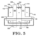
- the other channel/dielectric interface 120 remains. It is contemplated that the first leg 116 may extend over the bottom-edge 108, or as shown in Figure 5, stop at the second leg 118.
- a drain region 122 is defined by the first lateral edge 110 of the active region 102, the first leg 116, the top edge 106 of the active region 102, and the second leg 118.
- a source region 124 is defined by the second lateral edge 112 of the active region 102 and the L-shaped gate 117.
- the source region 124 and the drain region 122 have a first conductivity type (e.g., N), while the active region 102 under the first leg 116 and the second leg 118 has a second conductivity type (e.g., P).
- an implant region 130 having the second conductivity type extends from a portion of the first L-shaped gate 117 into the source region 124.
- the implant region 130 may be defined by mask 132.
- a silicide layer preferably formed using a conventional silicide process, is provided over at least a portion of the implant region 130 and the source region 124 to electrically connect the implant region 130 to the source region 124. Accordingly, a source contact 136 may be used to bias both the source 124 and the channel/body region of the transistor. As indicated above, this may increase the packing density of the device.
- the second leg 118 of the gate 117 may be spaced inward from the bottom edge 108 of the active region 102, as shown. This leaves a space 140 between the second leg 118 and the bottom edge 108 of the active region 102.
- the second leg 118 may overlap at least a portion of the bottom edge 108, which does not leave a space between the second leg 118 and the bottom edge of the active region 108.
- one of these embodiments may provide an increased packing density relative to the other.
- the second leg 118 may extend past the first leg 116 toward the second lateral edge 112 of the active region 102.
- the portion of the second leg 118 that extends past the first leg 116 may form a nub 150.
- the nub 150 increases the channel width along the side wall 152 that borders the second leg 118, which may help control the "effective" channel width of the device as described above.
- the overall gate area may be reduced relative to the T-gate and H-gate configurations shown in Figures 1 and 2. This may increase the speed and overall yield of the device.
- the spacing between two adjacent L-gate devices may be reduced relative to the prior art.
- FIG. 5 shows an enlarged top view of two L-gate MOSFETs in a common active region 200.
- the first L-shaped gate 117 is similar to that described above with respect to Figure 3.
- the second L-shaped gate 202 has a first leg 204 and a second leg 206.
- the first leg 204 of the second L-shaped gate 202 is spaced inward of the second lateral edge 112 and inward from the first L-shaped gate 117.
- the first leg 204 of the second L-shaped gate 202 preferably extends into the active region 200 over the top edge 106 of the active region 200.
- the first leg 204 may extend over the bottom edge 108, as shown at 220, or may stop at the second leg 206.
- the second leg 206 of the second L-shaped gate 202 is spaced inward from the top edge 106, and extends into the active region 200 over the second lateral edge 112 before intersecting the first leg 204.
- the second leg 206 preferably does not extend to the first L-shaped gate 117.
- a second drain region 210 is defined by the second lateral edge 112 of the active region 200, the first leg 204 of the second L-shaped gate 202, the top edge 106 of the active region 200, and the second leg 206 of the second L-shaped gate 202.
- the common source region 214 is defined by the space between the first L-shaped gate 117 and the second L-shaped gate 202.
- a second implant region which in the example shown is part of an enlarged first implant region 130, extends from a portion of the second L-shaped gate 202 into the common source region 214.
- a silicide layer (see Figure 8) or the like then extends over at least a portion of the second implant region 130 and over the common source region 214 for electrically connecting the second implant region 130 to the common source region 214.
- the second L-shaped gate 202 may be inverted relative to the first L-shaped gate 117. That is, the second leg 206 of the second L-shaped gate 202 may be positioned between the second drain region 210 and the upper edge 106 of the active region 200, if desired.
- FIG. 6 is an enlarged top view of an illustrative U-gate MOSFET.
- the illustrative U-gate MOSFET is generally shown at 300.
- the U-gate device 300 includes an active region 302 formed on an insulating layer and is surrounded by an isolation region 304.
- the active region has a top edge 306, a bottom edge 308, a first lateral edge 310, and a second lateral edge 312.
- a first leg 314 of the U-shaped gate 316 is preferably spaced inward of the first lateral edge 310 and inward of the second lateral edge 312 of the active region 302. If desired, the first leg 314 may extend over the top edge 306 and/or over the bottom edge 308 as best shown in Figure 7.
- a second leg 318 preferably extends into the active region 302 over the first lateral edge 310 and intersects the first leg 314, but does not extend to the second lateral edge 312.
- a third leg 320 spaced from the second leg 318, extends into the active region 302 over the first lateral edge 310 and intersects the first leg 314, but does not extend to the second lateral edge 312. Because the second leg 318 and third leg 320 do not extend to the second lateral edge 312, there is a space 322 between the U-shaped gate 316 and the second lateral edge 312.
- a drain region 326 is defined by the first lateral edge 310 of the active region 3.02, the first leg 314, the second leg 318, and the third leg 320.
- a source region 330 is defined by the second lateral edge 312 of the active region 302 and the U-shaped gate 316.
- the source region 330 and the drain region 326 preferably have a first conductivity type (e.g., N), and the active region 302 under the first leg 314, second leg 318 and third leg 320 have a second conductivity type (e.g., P).
- an implant region 332 having the second conductivity type (P) extends from a portion of the U-shaped gate 316 into the source region 330.
- a mask such as mask 334, is preferably used to define the implant region 332.
- a silicide layer or the like is then provided over at least a portion of the implant region 332 and the source region 330 to electrically connect the implant region 332 to the source region 330.
- the second leg 318 may be spaced inward of the top edge 206 of the active region 302, and the third leg 320 may be spaced inward of the bottom edge 308. This leaves a space 340 between the second leg 318 and the top edge 306, and a space 342 between the third leg 320 and the bottom edge 308 of the active region 302.
- the second leg 318 may overlap at least a portion of the top edge 306, and/or the third leg 320 may overlap at least a portion of the bottom edge 308 of the active region 302.
- This latter configuration does not leave any space between the second leg 318 and the top edge 306, or between the third leg 320 and the bottom edge 308 of the active region 302.
- one of these examples may provide an increased packing density over the other.
- the second leg 318 and third leg 320 may extend past the first leg 314 toward the second lateral edge 312 of the active region 302.
- the portion of the second leg 318 that extends past the first leg forms a first nub 350
- the portion of the third leg 320 that extends past the first leg 34 forms a second nub 352.
- the first nub 350 may help increase the channel width along the side wall 354 that borders the second leg 318
- the second nub 352 may help increase the channel width along the side wall 356 that borders the third leg 320.
- both the first nub 350 and the second nub 352 may help control the "effective" channel width of the device.
- the overall gate area may be reduced relative to the H-gate configuration shown in Figure 2. This may increase the speed and overall yield of the device.
- the spacing between two adjacent U-gate devices may be reduced relative to the H-gate configuration shown in Figure 2.
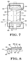
- Figure 8 is an enlarged cross-sectional view of the U-gate MOSFET of Figure 7 taken along line 8-8.
- a bottom insulating layer 383 supports the active region 302.
- the active region 302 includes the source region 330, the implant region 332 and the body/channel region 382. Because the implant region 332 is the same conductivity type as the body/channel region 382, the implant region 332 is electrically connected to the body/channel region 382.
- a silicide layer 384 is provided over the implant region 332 and the source region 330, and electrically connects the implant region 332 to the source region 330. Since the implant region 332 is electrically connected to the body/channel region 382, an electrical connection is made between the source region 330 and the body/channel region 382.
- a gate oxide layer 380 which supports the second leg 320.
- the second leg 320 is preferably a doped polysilicon material.
- a spacer 390 is preferably provided between the silicide layer 384 and the second leg 320.
- Another silicide layer 386 is preferably provided above the second leg 320 to lower the resistance thereof.
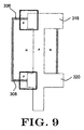
- FIG 10 is an enlarged top view of two illustrative U-gate MOSFETs in a common active region.
- the U-shaped gate may allow multiple transistors to be placed in the same active region, so long as they share a common source. This may help increase the packing density that can be achieved.
- the first U-shaped gate 316 may be similar to that described above with respect to Figures 6-9.
- the second U-shaped gate 400 may have a first leg 402, a second leg, 404, and a third leg 406.
- the first leg 402 is preferably spaced inward of the second lateral edge 312 and inward from the first U-shaped gate 316.
- the second leg 404 is preferably spaced inward from the top edge 306, and extends into the active region over the second lateral edge 312.
- the second leg 404 intersects the first leg 402 of the second U-shaped gate 400, but preferably does not extend to the first U-shaped gate 316.
- the third leg 406 is preferably spaced inward from the bottom edge 308, and extends into the active region over the second lateral edge 312.
- the third leg 406 intersects the first leg 402 of the second U-shaped gate 400, but does not extend to the first U-shaped gate 316.
- the second leg 404 and the third leg 406 may overlap at least a portion of the top and bottom edges 306 and 308, respectively.
- a second drain region 420 is defined by the second lateral edge 312 of the active region, the first leg 402, the second leg 404, and the third leg 4-6 of the second U-shaped gate 400.
- a common source region 422 extends between the second U-shaped gate 400 and the first U-shaped gate 316.
- a second implant region 332, which in the embodiment shown is part of an enlarged first implant region, may extend from a portion of the second U-shaped gate 400 and into the common source region 422.
- a silicide layer or the like may then extend over at least a portion of the second implant region 332 and over the common source region 422 for electrically connecting the second implant region 332 to the common source region 422.
Landscapes
- Thin Film Transistor (AREA)
- Steering-Linkage Mechanisms And Four-Wheel Steering (AREA)
- Superconductors And Manufacturing Methods Therefor (AREA)
- Surface Acoustic Wave Elements And Circuit Networks Thereof (AREA)
- Metal-Oxide And Bipolar Metal-Oxide Semiconductor Integrated Circuits (AREA)
- Insulated Gate Type Field-Effect Transistor (AREA)
Priority Applications (1)
| Application Number | Priority Date | Filing Date | Title |
|---|---|---|---|
| EP07101360A EP1783836A3 (en) | 1999-12-28 | 2000-12-18 | L- and U-gate devices for SOI/SOS applications |
Applications Claiming Priority (3)
| Application Number | Priority Date | Filing Date | Title |
|---|---|---|---|
| US473158 | 1999-12-28 | ||
| US09/473,158 US6307237B1 (en) | 1999-12-28 | 1999-12-28 | L-and U-gate devices for SOI/SOS applications |
| PCT/US2000/034249 WO2001048828A1 (en) | 1999-12-28 | 2000-12-18 | L- and u-gate devices for soi/sos applications |
Related Child Applications (1)
| Application Number | Title | Priority Date | Filing Date |
|---|---|---|---|
| EP07101360A Division EP1783836A3 (en) | 1999-12-28 | 2000-12-18 | L- and U-gate devices for SOI/SOS applications |
Publications (2)
| Publication Number | Publication Date |
|---|---|
| EP1243028A1 EP1243028A1 (en) | 2002-09-25 |
| EP1243028B1 true EP1243028B1 (en) | 2007-04-18 |
Family
ID=23878441
Family Applications (2)
| Application Number | Title | Priority Date | Filing Date |
|---|---|---|---|
| EP07101360A Withdrawn EP1783836A3 (en) | 1999-12-28 | 2000-12-18 | L- and U-gate devices for SOI/SOS applications |
| EP00988112A Expired - Lifetime EP1243028B1 (en) | 1999-12-28 | 2000-12-18 | L- and u-gate devices for soi/sos applications |
Family Applications Before (1)
| Application Number | Title | Priority Date | Filing Date |
|---|---|---|---|
| EP07101360A Withdrawn EP1783836A3 (en) | 1999-12-28 | 2000-12-18 | L- and U-gate devices for SOI/SOS applications |
Country Status (6)
| Country | Link |
|---|---|
| US (1) | US6307237B1 (enExample) |
| EP (2) | EP1783836A3 (enExample) |
| JP (1) | JP2003518775A (enExample) |
| AT (1) | ATE360261T1 (enExample) |
| DE (1) | DE60034483T2 (enExample) |
| WO (1) | WO2001048828A1 (enExample) |
Families Citing this family (34)
| Publication number | Priority date | Publication date | Assignee | Title |
|---|---|---|---|---|
| JP3716406B2 (ja) * | 2000-02-08 | 2005-11-16 | 富士通株式会社 | 絶縁ゲート型半導体装置及びその製造方法 |
| US6483156B1 (en) * | 2000-03-16 | 2002-11-19 | International Business Machines Corporation | Double planar gated SOI MOSFET structure |
| US20030036236A1 (en) * | 2001-08-15 | 2003-02-20 | Joseph Benedetto | Method for radiation hardening N-channel MOS transistors |
| US6642579B2 (en) * | 2001-08-28 | 2003-11-04 | International Business Machines Corporation | Method of reducing the extrinsic body resistance in a silicon-on-insulator body contacted MOSFET |
| JP4044446B2 (ja) * | 2002-02-19 | 2008-02-06 | セイコーインスツル株式会社 | 半導体装置およびその製造方法 |
| US6960810B2 (en) * | 2002-05-30 | 2005-11-01 | Honeywell International Inc. | Self-aligned body tie for a partially depleted SOI device structure |
| US20030222308A1 (en) * | 2002-05-30 | 2003-12-04 | Taiwan Semiconductor Manufacturing Co., Ltd. | SOI MOSFET with compact body-tied-source structure |
| US6861716B1 (en) * | 2003-10-31 | 2005-03-01 | International Business Machines Corporation | Ladder-type gate structure for four-terminal SOI semiconductor device |
| US7084462B1 (en) * | 2005-04-15 | 2006-08-01 | International Business Machines Corporation | Parallel field effect transistor structure having a body contact |
| US20070090431A1 (en) * | 2005-10-24 | 2007-04-26 | Honeywell International Inc. | Device layout for reducing device upset due to single event effects |
| KR100654053B1 (ko) * | 2005-12-29 | 2006-12-05 | 동부일렉트로닉스 주식회사 | 부가 게이트 도체 패턴을 갖는 협채널 금속 산화물 반도체트랜지스터 |
| KR101219464B1 (ko) * | 2007-07-23 | 2013-01-11 | 삼성전자주식회사 | 반도체 장치 및 그 제조 방법 |
| US8410554B2 (en) * | 2008-03-26 | 2013-04-02 | International Business Machines Corporation | Method, structure and design structure for customizing history effects of SOI circuits |
| US7964467B2 (en) * | 2008-03-26 | 2011-06-21 | International Business Machines Corporation | Method, structure and design structure for customizing history effects of soi circuits |
| US8420460B2 (en) | 2008-03-26 | 2013-04-16 | International Business Machines Corporation | Method, structure and design structure for customizing history effects of SOI circuits |
| GB2460395A (en) * | 2008-04-29 | 2009-12-02 | Sharp Kk | Thin film transistor and active matrix display |
| GB2459666A (en) * | 2008-04-29 | 2009-11-04 | Sharp Kk | Thin film transistor with low leakage current |
| JP5555864B2 (ja) * | 2009-12-22 | 2014-07-23 | 株式会社ブルックマンテクノロジ | 絶縁ゲート型半導体素子及び絶縁ゲート型半導体集積回路 |
| CN101931008B (zh) * | 2010-07-13 | 2015-04-08 | 中国科学院上海微系统与信息技术研究所 | 一种具有体接触结构的pd soi器件 |
| US8217456B1 (en) | 2011-03-11 | 2012-07-10 | International Business Machines Corporation | Low capacitance hi-K dual work function metal gate body-contacted field effect transistor |
| JP6184057B2 (ja) * | 2012-04-18 | 2017-08-23 | ルネサスエレクトロニクス株式会社 | 半導体装置 |
| US20140103440A1 (en) * | 2012-10-15 | 2014-04-17 | Texas Instruments Incorporated | I-shaped gate electrode for improved sub-threshold mosfet performance |
| US20170141134A1 (en) * | 2015-11-18 | 2017-05-18 | Peregrine Semiconductor Corporation | Butted Body Contact for SOI Transistor |
| US9842858B2 (en) | 2015-11-18 | 2017-12-12 | Peregrine Semiconductor Corporation | Butted body contact for SOI transistor |
| CN114122141A (zh) * | 2016-03-23 | 2022-03-01 | 派赛公司 | 半导体结构和用于向共源共栅晶体管提供本体连结的方法 |
| US9837965B1 (en) | 2016-09-16 | 2017-12-05 | Peregrine Semiconductor Corporation | Standby voltage condition for fast RF amplifier bias recovery |
| FR3056331B1 (fr) * | 2016-09-19 | 2018-10-26 | Stmicroelectronics Sa | Polarisation de la region de substrat d'un transistor mos |
| US10424664B2 (en) | 2016-12-14 | 2019-09-24 | Globalfoundries Inc. | Poly gate extension source to body contact |
| US9960737B1 (en) | 2017-03-06 | 2018-05-01 | Psemi Corporation | Stacked PA power control |
| FR3076398B1 (fr) * | 2017-12-29 | 2019-12-27 | X-Fab France | Transistor et son procede de fabrication |
| US11444169B2 (en) | 2020-02-27 | 2022-09-13 | Taiwan Semiconductor Manufacturing Company, Ltd. | Transistor device with a gate structure having recesses overlying an interface between isolation and device regions |
| CN113314610B (zh) | 2020-02-27 | 2024-04-30 | 台湾积体电路制造股份有限公司 | 晶体管器件及其制造方法 |
| US11476279B2 (en) | 2020-08-06 | 2022-10-18 | Globalfoundries U.S. Inc. | Devices with staggered body contacts |
| CN114188408A (zh) * | 2020-09-14 | 2022-03-15 | 联华电子股份有限公司 | 半导体元件 |
Family Cites Families (12)
| Publication number | Priority date | Publication date | Assignee | Title |
|---|---|---|---|---|
| JPS6021542A (ja) * | 1983-07-15 | 1985-02-02 | Toshiba Corp | 半導体集積回路装置 |
| JPH0379035A (ja) * | 1989-08-22 | 1991-04-04 | Nippondenso Co Ltd | Mosトランジスタ及びその製造方法 |
| US5217915A (en) * | 1991-04-08 | 1993-06-08 | Texas Instruments Incorporated | Method of making gate array base cell |
| USH1435H (en) | 1991-10-21 | 1995-05-02 | Cherne Richard D | SOI CMOS device having body extension for providing sidewall channel stop and bodytie |
| US5298773A (en) | 1992-08-17 | 1994-03-29 | United Technologies Corporation | Silicon-on-insulator H-transistor layout for gate arrays |
| US5317181A (en) | 1992-09-10 | 1994-05-31 | United Technologies Corporation | Alternative body contact for fully-depleted silicon-on-insulator transistors |
| US5334545A (en) | 1993-02-01 | 1994-08-02 | Allied Signal Inc. | Process for forming self-aligning cobalt silicide T-gates of silicon MOS devices |
| JP3364559B2 (ja) * | 1995-10-11 | 2003-01-08 | 三菱電機株式会社 | 半導体装置 |
| US5821575A (en) | 1996-05-20 | 1998-10-13 | Digital Equipment Corporation | Compact self-aligned body contact silicon-on-insulator transistor |
| US5920093A (en) | 1997-04-07 | 1999-07-06 | Motorola, Inc. | SOI FET having gate sub-regions conforming to t-shape |
| KR100252913B1 (ko) * | 1997-04-21 | 2000-04-15 | 김영환 | 반도체 소자 및 그 제조방법 |
| US5811855A (en) | 1997-12-29 | 1998-09-22 | United Technologies Corporation | SOI combination body tie |
-
1999
- 1999-12-28 US US09/473,158 patent/US6307237B1/en not_active Expired - Lifetime
-
2000
- 2000-12-18 AT AT00988112T patent/ATE360261T1/de not_active IP Right Cessation
- 2000-12-18 WO PCT/US2000/034249 patent/WO2001048828A1/en not_active Ceased
- 2000-12-18 DE DE60034483T patent/DE60034483T2/de not_active Expired - Lifetime
- 2000-12-18 EP EP07101360A patent/EP1783836A3/en not_active Withdrawn
- 2000-12-18 JP JP2001548446A patent/JP2003518775A/ja active Pending
- 2000-12-18 EP EP00988112A patent/EP1243028B1/en not_active Expired - Lifetime
Also Published As
| Publication number | Publication date |
|---|---|
| EP1783836A3 (en) | 2008-02-27 |
| ATE360261T1 (de) | 2007-05-15 |
| EP1783836A2 (en) | 2007-05-09 |
| JP2003518775A (ja) | 2003-06-10 |
| DE60034483T2 (de) | 2008-01-03 |
| EP1243028A1 (en) | 2002-09-25 |
| US6307237B1 (en) | 2001-10-23 |
| DE60034483D1 (de) | 2007-05-31 |
| WO2001048828A1 (en) | 2001-07-05 |
Similar Documents
| Publication | Publication Date | Title |
|---|---|---|
| EP1243028B1 (en) | L- and u-gate devices for soi/sos applications | |
| USH1435H (en) | SOI CMOS device having body extension for providing sidewall channel stop and bodytie | |
| US5185280A (en) | Method of fabricating a soi transistor with pocket implant and body-to-source (bts) contact | |
| KR100343288B1 (ko) | 에스오아이 모스 트랜지스터의 플로팅 바디 효과를제거하기 위한 에스오아이 반도체 집적회로 및 그 제조방법 | |
| US6521959B2 (en) | SOI semiconductor integrated circuit for eliminating floating body effects in SOI MOSFETs and method of fabricating the same | |
| JP3364559B2 (ja) | 半導体装置 | |
| KR101144025B1 (ko) | 반도체 장치 및 그 제조 방법 | |
| KR100374627B1 (ko) | 고내압 아이솔레이션 영역을 갖는 고전압 반도체 소자 | |
| TW201733126A (zh) | 半導體器件 | |
| JP2001102586A (ja) | 高耐圧半導体装置 | |
| US4885618A (en) | Insulated gate FET having a buried insulating barrier | |
| JP2633145B2 (ja) | 半導体横方向絶縁ゲートバイポーラトランジスタ装置 | |
| KR100335527B1 (ko) | 정전보호회로로서형성되는반도체소자 | |
| US7619287B2 (en) | Method of forming a low capacitance semiconductor device and structure therefor | |
| US6525392B1 (en) | Semiconductor power device with insulated circuit | |
| US20240405015A1 (en) | Semiconductor device with esd protection structure and method of making same | |
| KR100374628B1 (ko) | 고내압 아이솔레이션 영역을 갖는 고전압 반도체소자 | |
| JP2004288873A (ja) | 半導体装置 | |
| KR100694327B1 (ko) | 반도체 디바이스 | |
| JPH0760901B2 (ja) | 半導体装置 | |
| JPH07221314A (ja) | Soi構造mos型半導体装置 | |
| JPH0563024B2 (enExample) | ||
| JPH02260538A (ja) | 半導体装置 | |
| JP2004055940A (ja) | 横型mosトランジスタ | |
| KR19980039577A (ko) | 전력 트랜지스터 및 그 제조 방법 |
Legal Events
| Date | Code | Title | Description |
|---|---|---|---|
| PUAI | Public reference made under article 153(3) epc to a published international application that has entered the european phase |
Free format text: ORIGINAL CODE: 0009012 |
|
| 17P | Request for examination filed |
Effective date: 20020625 |
|
| AK | Designated contracting states |
Kind code of ref document: A1 Designated state(s): AT BE CH CY DE DK ES FI FR GB GR IE IT LI LU MC NL PT SE TR |
|
| 17Q | First examination report despatched |
Effective date: 20050602 |
|
| GRAP | Despatch of communication of intention to grant a patent |
Free format text: ORIGINAL CODE: EPIDOSNIGR1 |
|
| GRAS | Grant fee paid |
Free format text: ORIGINAL CODE: EPIDOSNIGR3 |
|
| GRAA | (expected) grant |
Free format text: ORIGINAL CODE: 0009210 |
|
| AK | Designated contracting states |
Kind code of ref document: B1 Designated state(s): AT BE CH CY DE DK ES FI FR GB GR IE IT LI LU MC NL PT SE TR |
|
| PG25 | Lapsed in a contracting state [announced via postgrant information from national office to epo] |
Ref country code: FI Free format text: LAPSE BECAUSE OF FAILURE TO SUBMIT A TRANSLATION OF THE DESCRIPTION OR TO PAY THE FEE WITHIN THE PRESCRIBED TIME-LIMIT Effective date: 20070418 Ref country code: CH Free format text: LAPSE BECAUSE OF FAILURE TO SUBMIT A TRANSLATION OF THE DESCRIPTION OR TO PAY THE FEE WITHIN THE PRESCRIBED TIME-LIMIT Effective date: 20070418 Ref country code: LI Free format text: LAPSE BECAUSE OF FAILURE TO SUBMIT A TRANSLATION OF THE DESCRIPTION OR TO PAY THE FEE WITHIN THE PRESCRIBED TIME-LIMIT Effective date: 20070418 |
|
| REG | Reference to a national code |
Ref country code: CH Ref legal event code: EP |
|
| REG | Reference to a national code |
Ref country code: IE Ref legal event code: FG4D |
|
| REF | Corresponds to: |
Ref document number: 60034483 Country of ref document: DE Date of ref document: 20070531 Kind code of ref document: P |
|
| PG25 | Lapsed in a contracting state [announced via postgrant information from national office to epo] |
Ref country code: SE Free format text: LAPSE BECAUSE OF FAILURE TO SUBMIT A TRANSLATION OF THE DESCRIPTION OR TO PAY THE FEE WITHIN THE PRESCRIBED TIME-LIMIT Effective date: 20070718 |
|
| PG25 | Lapsed in a contracting state [announced via postgrant information from national office to epo] |
Ref country code: ES Free format text: LAPSE BECAUSE OF FAILURE TO SUBMIT A TRANSLATION OF THE DESCRIPTION OR TO PAY THE FEE WITHIN THE PRESCRIBED TIME-LIMIT Effective date: 20070729 |
|
| ET | Fr: translation filed | ||
| PG25 | Lapsed in a contracting state [announced via postgrant information from national office to epo] |
Ref country code: PT Free format text: LAPSE BECAUSE OF FAILURE TO SUBMIT A TRANSLATION OF THE DESCRIPTION OR TO PAY THE FEE WITHIN THE PRESCRIBED TIME-LIMIT Effective date: 20070918 |
|
| REG | Reference to a national code |
Ref country code: CH Ref legal event code: PL |
|
| NLV1 | Nl: lapsed or annulled due to failure to fulfill the requirements of art. 29p and 29m of the patents act | ||
| PG25 | Lapsed in a contracting state [announced via postgrant information from national office to epo] |
Ref country code: AT Free format text: LAPSE BECAUSE OF FAILURE TO SUBMIT A TRANSLATION OF THE DESCRIPTION OR TO PAY THE FEE WITHIN THE PRESCRIBED TIME-LIMIT Effective date: 20070418 |
|
| PG25 | Lapsed in a contracting state [announced via postgrant information from national office to epo] |
Ref country code: BE Free format text: LAPSE BECAUSE OF FAILURE TO SUBMIT A TRANSLATION OF THE DESCRIPTION OR TO PAY THE FEE WITHIN THE PRESCRIBED TIME-LIMIT Effective date: 20070418 |
|
| PG25 | Lapsed in a contracting state [announced via postgrant information from national office to epo] |
Ref country code: DK Free format text: LAPSE BECAUSE OF FAILURE TO SUBMIT A TRANSLATION OF THE DESCRIPTION OR TO PAY THE FEE WITHIN THE PRESCRIBED TIME-LIMIT Effective date: 20070418 Ref country code: NL Free format text: LAPSE BECAUSE OF FAILURE TO SUBMIT A TRANSLATION OF THE DESCRIPTION OR TO PAY THE FEE WITHIN THE PRESCRIBED TIME-LIMIT Effective date: 20070418 |
|
| PLBE | No opposition filed within time limit |
Free format text: ORIGINAL CODE: 0009261 |
|
| STAA | Information on the status of an ep patent application or granted ep patent |
Free format text: STATUS: NO OPPOSITION FILED WITHIN TIME LIMIT |
|
| 26N | No opposition filed |
Effective date: 20080121 |
|
| PG25 | Lapsed in a contracting state [announced via postgrant information from national office to epo] |
Ref country code: GR Free format text: LAPSE BECAUSE OF FAILURE TO SUBMIT A TRANSLATION OF THE DESCRIPTION OR TO PAY THE FEE WITHIN THE PRESCRIBED TIME-LIMIT Effective date: 20070719 Ref country code: IT Free format text: LAPSE BECAUSE OF FAILURE TO SUBMIT A TRANSLATION OF THE DESCRIPTION OR TO PAY THE FEE WITHIN THE PRESCRIBED TIME-LIMIT Effective date: 20070418 |
|
| PG25 | Lapsed in a contracting state [announced via postgrant information from national office to epo] |
Ref country code: MC Free format text: LAPSE BECAUSE OF NON-PAYMENT OF DUE FEES Effective date: 20071231 |
|
| PG25 | Lapsed in a contracting state [announced via postgrant information from national office to epo] |
Ref country code: IE Free format text: LAPSE BECAUSE OF NON-PAYMENT OF DUE FEES Effective date: 20071218 |
|
| PG25 | Lapsed in a contracting state [announced via postgrant information from national office to epo] |
Ref country code: CY Free format text: LAPSE BECAUSE OF FAILURE TO SUBMIT A TRANSLATION OF THE DESCRIPTION OR TO PAY THE FEE WITHIN THE PRESCRIBED TIME-LIMIT Effective date: 20070418 |
|
| PG25 | Lapsed in a contracting state [announced via postgrant information from national office to epo] |
Ref country code: LU Free format text: LAPSE BECAUSE OF NON-PAYMENT OF DUE FEES Effective date: 20071218 |
|
| PG25 | Lapsed in a contracting state [announced via postgrant information from national office to epo] |
Ref country code: TR Free format text: LAPSE BECAUSE OF FAILURE TO SUBMIT A TRANSLATION OF THE DESCRIPTION OR TO PAY THE FEE WITHIN THE PRESCRIBED TIME-LIMIT Effective date: 20070418 |
|
| PGFP | Annual fee paid to national office [announced via postgrant information from national office to epo] |
Ref country code: DE Payment date: 20121221 Year of fee payment: 13 |
|
| REG | Reference to a national code |
Ref country code: DE Ref legal event code: R119 Ref document number: 60034483 Country of ref document: DE |
|
| REG | Reference to a national code |
Ref country code: DE Ref legal event code: R119 Ref document number: 60034483 Country of ref document: DE Effective date: 20140701 |
|
| PG25 | Lapsed in a contracting state [announced via postgrant information from national office to epo] |
Ref country code: DE Free format text: LAPSE BECAUSE OF NON-PAYMENT OF DUE FEES Effective date: 20140701 |
|
| REG | Reference to a national code |
Ref country code: FR Ref legal event code: PLFP Year of fee payment: 16 |
|
| PGFP | Annual fee paid to national office [announced via postgrant information from national office to epo] |
Ref country code: GB Payment date: 20151125 Year of fee payment: 16 |
|
| PGFP | Annual fee paid to national office [announced via postgrant information from national office to epo] |
Ref country code: FR Payment date: 20151124 Year of fee payment: 16 |
|
| GBPC | Gb: european patent ceased through non-payment of renewal fee |
Effective date: 20161218 |
|
| REG | Reference to a national code |
Ref country code: FR Ref legal event code: ST Effective date: 20170831 |
|
| PG25 | Lapsed in a contracting state [announced via postgrant information from national office to epo] |
Ref country code: FR Free format text: LAPSE BECAUSE OF NON-PAYMENT OF DUE FEES Effective date: 20170102 |
|
| PG25 | Lapsed in a contracting state [announced via postgrant information from national office to epo] |
Ref country code: GB Free format text: LAPSE BECAUSE OF NON-PAYMENT OF DUE FEES Effective date: 20161218 |