EP1222325B1 - Method for producing czochralski silicon free of agglomerated self-interstitial defects - Google Patents
Method for producing czochralski silicon free of agglomerated self-interstitial defects Download PDFInfo
- Publication number
- EP1222325B1 EP1222325B1 EP00961957A EP00961957A EP1222325B1 EP 1222325 B1 EP1222325 B1 EP 1222325B1 EP 00961957 A EP00961957 A EP 00961957A EP 00961957 A EP00961957 A EP 00961957A EP 1222325 B1 EP1222325 B1 EP 1222325B1
- Authority
- EP
- European Patent Office
- Prior art keywords
- defects
- seconds
- time period
- wafer
- silicon
- Prior art date
- Legal status (The legal status is an assumption and is not a legal conclusion. Google has not performed a legal analysis and makes no representation as to the accuracy of the status listed.)
- Expired - Lifetime
Links
Images
Classifications
-
- C—CHEMISTRY; METALLURGY
- C30—CRYSTAL GROWTH
- C30B—SINGLE-CRYSTAL GROWTH; UNIDIRECTIONAL SOLIDIFICATION OF EUTECTIC MATERIAL OR UNIDIRECTIONAL DEMIXING OF EUTECTOID MATERIAL; REFINING BY ZONE-MELTING OF MATERIAL; PRODUCTION OF A HOMOGENEOUS POLYCRYSTALLINE MATERIAL WITH DEFINED STRUCTURE; SINGLE CRYSTALS OR HOMOGENEOUS POLYCRYSTALLINE MATERIAL WITH DEFINED STRUCTURE; AFTER-TREATMENT OF SINGLE CRYSTALS OR A HOMOGENEOUS POLYCRYSTALLINE MATERIAL WITH DEFINED STRUCTURE; APPARATUS THEREFOR
- C30B33/00—After-treatment of single crystals or homogeneous polycrystalline material with defined structure
- C30B33/02—Heat treatment
-
- C—CHEMISTRY; METALLURGY
- C30—CRYSTAL GROWTH
- C30B—SINGLE-CRYSTAL GROWTH; UNIDIRECTIONAL SOLIDIFICATION OF EUTECTIC MATERIAL OR UNIDIRECTIONAL DEMIXING OF EUTECTOID MATERIAL; REFINING BY ZONE-MELTING OF MATERIAL; PRODUCTION OF A HOMOGENEOUS POLYCRYSTALLINE MATERIAL WITH DEFINED STRUCTURE; SINGLE CRYSTALS OR HOMOGENEOUS POLYCRYSTALLINE MATERIAL WITH DEFINED STRUCTURE; AFTER-TREATMENT OF SINGLE CRYSTALS OR A HOMOGENEOUS POLYCRYSTALLINE MATERIAL WITH DEFINED STRUCTURE; APPARATUS THEREFOR
- C30B29/00—Single crystals or homogeneous polycrystalline material with defined structure characterised by the material or by their shape
- C30B29/02—Elements
- C30B29/06—Silicon
-
- C—CHEMISTRY; METALLURGY
- C30—CRYSTAL GROWTH
- C30B—SINGLE-CRYSTAL GROWTH; UNIDIRECTIONAL SOLIDIFICATION OF EUTECTIC MATERIAL OR UNIDIRECTIONAL DEMIXING OF EUTECTOID MATERIAL; REFINING BY ZONE-MELTING OF MATERIAL; PRODUCTION OF A HOMOGENEOUS POLYCRYSTALLINE MATERIAL WITH DEFINED STRUCTURE; SINGLE CRYSTALS OR HOMOGENEOUS POLYCRYSTALLINE MATERIAL WITH DEFINED STRUCTURE; AFTER-TREATMENT OF SINGLE CRYSTALS OR A HOMOGENEOUS POLYCRYSTALLINE MATERIAL WITH DEFINED STRUCTURE; APPARATUS THEREFOR
- C30B15/00—Single-crystal growth by pulling from a melt, e.g. Czochralski method
- C30B15/20—Controlling or regulating
- C30B15/206—Controlling or regulating the thermal history of growing the ingot
-
- C—CHEMISTRY; METALLURGY
- C30—CRYSTAL GROWTH
- C30B—SINGLE-CRYSTAL GROWTH; UNIDIRECTIONAL SOLIDIFICATION OF EUTECTIC MATERIAL OR UNIDIRECTIONAL DEMIXING OF EUTECTOID MATERIAL; REFINING BY ZONE-MELTING OF MATERIAL; PRODUCTION OF A HOMOGENEOUS POLYCRYSTALLINE MATERIAL WITH DEFINED STRUCTURE; SINGLE CRYSTALS OR HOMOGENEOUS POLYCRYSTALLINE MATERIAL WITH DEFINED STRUCTURE; AFTER-TREATMENT OF SINGLE CRYSTALS OR A HOMOGENEOUS POLYCRYSTALLINE MATERIAL WITH DEFINED STRUCTURE; APPARATUS THEREFOR
- C30B33/00—After-treatment of single crystals or homogeneous polycrystalline material with defined structure
Definitions
- the present invention generally relates to the preparation of semiconductor material substrates, especially silicon wafers, which are used in the manufacture of electronic components. More particularly, the present invention relates to a heat treatment process for annihilating B-type silicon self-interstitial agglomerated defects in single crystal silicon.
- Single crystal silicon which is the starting material for most processes for the fabrication of semiconductor electronic components, is commonly prepared by the so-called Czochralski (“Cz”) method.
- Cz Czochralski
- polycrystalline silicon (“polysilicon”) is charged to a crucible and melted, a seed crystal is brought into contact with the molten silicon, and then a single crystal is grown by slow extraction. After formation of a neck is complete, the diameter of the crystal is enlarged by decreasing the pulling rate and/or the melt temperature until the desired or target diameter is reached. The cylindrical main body of the crystal which has an approximately constant diameter is then grown by controlling the pull rate and the melt temperature while compensating for the decreasing melt level.
- the crystal diameter must be reduced gradually to form an end-cone.
- the end-cone is formed by increasing the crystal pull rate and heat supplied to the crucible. When the diameter becomes small enough, the crystal is then separated from the melt.
- Vacancy-type defects are recognized to be the origin of such observable crystal defects as D-defects, Flow Pattern Defects (FPDs), Gate Oxide Integrity (GOI) Defects, Crystal Originated Particle (COP) Defects, crystal originated Light Point Defects (LPDs), as well as certain classes of bulk defects observed by infrared light scattering techniques, such as Scanning Infrared Microscopy and Laser Scanning Tomography. Also present in regions of excess vacancies are defects which act as the nuclei for ring oxidation induced stacking faults (OISF). It is speculated that this particular defect is a high temperature nucleated oxygen agglomerate catalyzed by the presence of excess vacancies.
- A-defects and B-defects are more well studied, however, two types of self-interstitial defects have been observed and are commonly referred to as A-defects and B-defects (or A- and B- "swirls" or “clusters”).
- A-defects are larger and more easily detected by means common in the art, as compared to B-defects.
- A-defects are generally regarded as being low densities of interstitial-type dislocation loops or networks. Less is known about B-defects, primarily because they are much smaller in size and also because, until recently, methods for easily and reliably detecting such defects have not existed.
- the International Patent Application WO 98/45508 relates to the preparation of semiconductor grade single crystal silicon having an axially symmetric region of vacancy dominated material which is devoid of agglomerated intrinsic point defects and a process for the preparation thereof.
- high temperature heat treatments of silicon wafers are discussed.
- A- and B-defects are not believed to be responsible for gate oxide integrity failures, an important wafer performance criterion, A-defects at least are widely recognized to be the cause of other types of device failures usually associated with current leakage problems. Less is known about the problems associated with B-defects. However, as device technology continues to improve, thus enabling the preparation of even smaller integrated circuitry, these smaller interstitial defects will naturally become the focus of greater concern. Accordingly, a need continues to exist for the means by which to prepare silicon wafers which are free of both A-type and B-type agglomerated interstitial defects.
- the provision of a process of annihilating B-defects from single crystal silicon the provision of a process for producing a single crystal silicon wafer which is substantially free of B-defects; the provision of a process wherein a silicon wafer substantially free of A-defects is rendered substantially free of B-defects; the provision of a single crystal silicon wafer substantially free of both A- and B-defects; and, the provision of a process for producing an ideal precipitating single crystal silicon wafer which is substantially free of B-defects.
- the present invention is directed to a process for heat treating a silicon wafer to dissolve B-defects present therein.
- the process comprises subjecting the wafer to a B-defect dissolution heat-treatment, wherein the wafer temperature is increased through a range of temperatures at which B-defects can grow and can become stabilized, at a heating rate sufficient to prevent the stabilization of the B-defects to a heat-treatment temperature of at least about 1000 °C and maintaining the wafer at the heat-treatment temperature for a time period sufficient to dissolve the B-defects.
- the present invention is further directed to a process for heat-treating a single crystal silicon wafer to dissolve B-defects and to influence the precipitation behavior of oxygen in the wafer in a subsequent thermal processing step.
- the process comprises subjecting the wafer to a B-defect dissolution heat-treatment, wherein the wafer temperature is increased through a range of temperatures at which B-defects can grow and can become stabilized, at a heating rate sufficient to prevent the stabilization of the B-defects to a heat-treatment temperature of at least about 1000 °C.
- B-type agglomerated silicon self-interstitial intrinsic point defects (hereinafter B-defects) in single crystal silicon may be dissolved, or annihilated, by heat treating the silicon containing them.
- A-type agglomerated silicon self-interstitial intrinsic point defects (hereinafter A-defects) are formed when agglomerations of interstitial defects collapse to form dislocation loops or stacking faults.
- B-defects are smaller in size as compared to A-defects and are generally believed to be agglomerations which have either not grown large enough or not reached a sufficient activation energy, such that dislocation loops or stacking faults are formed.
- B-defects may be dissolved by heating the silicon, effectively causing these defects to disassociate into independent silicon self-interstitials, the resulting silicon self-interstitials rapidly diffusing to the silicon surface.
- the rapid "out diffusion" of interstitials acts to lower the overall concentration of interstitials such that, upon subsequent cooling of the silicon, re-agglomeration does not occur, effectively rendering the silicon substantially free of B-defects.
- the starting material for the process of the present invention may be any silicon in which B-defects are present.
- the starting material is a single crystal silicon wafer having a central axis, a front side and a back side which are generally perpendicular to the central axis, a circumferential edge, and a radius extending from the central axis to the circumferential edge of the wafer of at least about 25, 50, 75, 100, or 150 mm or greater, which has been sliced from a single crystal ingot grown in accordance with conventional Czochralski crystal growing methods.
- the wafer may be a polished silicon wafer, or alternatively, a silicon wafer which has been lapped and etched but not polished.
- the wafer may have different axially symmetric regions in which vacancy or self-interstitial point defects are the predominant intrinsic point defect.
- the wafer may be self-interstitial dominated from center to edge, or it may contain a central core of vacancy dominated material surrounded by an axially symmetric ring of self-interstitial dominated material.
- the starting material is a single crystal silicon wafer which is self-interstitial dominated from center to edge and which is substantially free of A-defects (see, e.g., WO 98/45510 and WO 98/45509.
- a single crystal silicon wafer is subjected to a heat-treatment step in which the wafer is heated to a temperature of at least about 1000 °C for a time sufficient to dissolve B-defects, effectively rendering the wafer substantially free of such defects.
- B-defects cannot be dissolved if these defects have first been subjected to a stabilizing thermal treatment.
- experience to-date suggests that annealing the silicon at a temperature ranging from about 500°C to less than about 1000°C for about two to about four hours or greater can stabilize the B-defects, such that they are incapable of being dissolved. It is to be noted in this regard, however, that B-defects may be stabilized if exposed to temperatures less than about 500°C. However, exposure times greater than about 4 hours would be required. It is to be further noted that exposure to temperatures ranging from about 900°C to about 1000 °C may result in the growth and eventual transformation of B-defects into A-defects, at which point these defects are also rendered incapable of being dissolved.
- B-defects are dissolved in accordance with the present process by ensuring that the silicon which contains them is heated to a temperature and for a time sufficient to dissolve these defects, while ensuring the silicon is not first exposed to conditions which would result in their stabilization. More specifically, in accordance with the present process, a silicon sample is heated to a temperature in excess of about 1000°C (i.e., a temperature sufficient to dissolve B-defects), while ensuring that the rate at which the silicon reaches this temperature is not such that the B-defects are effectively stabilized against dissolution in the process. Generally speaking, the silicon is heated to a temperature in excess of about 1000°C, preferably about 1100°C, more preferably about 1150°C, still more preferably about 1200°C, and most preferably about 1250°C.
- the silicon sample is maintained at the target temperature for a time period sufficient to dissolve B-defects which are present.
- the sample may be heated in a rapid thermal annealer for a few seconds (e.g., at least about 2, 3, 5 or more), several tens of seconds (e.g., 10, 20, 30, 40, 50 or more) or, depending upon the desired characteristics of the wafer and the target temperature, for a period of up to about 60 seconds (which is near the limit of commercially available rapid thermal annealers).
- longer time periods for the heat treatment correspond to lower temperatures and vice versa. Accordingly, a wafer heated to a temperature of 1000 °C will take considerably longer for the B-defects to dissolve than a wafer heated to a temperature of, for example, 1200°C.
- the time and temperature combination sufficient for B-defect dissolution may be determined empirically by, for example, heating a series of wafers at a given temperature for varying periods of time and then analyzing the wafers, as further described below, in order to determine if B-defects are present.
- the temperature of the wafer is typically increased at a rate, through the range of temperatures at which stabilization of B-defects can occur, which is sufficient to avoid this stabilization; that is, the wafer is typically heated at a rate which ensures it is not exposed to a temperature ranging from about 500°C to less than about 1000°C for a time period sufficient to result in the stabilization of B-defects. Accordingly, preferably the temperature is increased at a rate of at least about 5°C/second, more preferably at least about 10°C/second, still more preferably at least about 15°C/second, still more preferably at least about 20°C/second, and most preferably at least about 25°C/second.
- the heat treatment may be carried out in any of a number of commercially available rapid thermal annealing ("RTA") furnaces in which wafers are individually heated by banks of high power lamps.
- RTA furnaces are capable of rapidly heating a silicon wafer, e.g., they are capable of heating a wafer from room temperature to 1200 °C in a few seconds.
- One such commercially available RTA furnace is the model 610 furnace available from AG Associates (Mountain View, CA).
- an ideal precipitating wafer which is substantially free from B-defects is produced. More specifically, an ideal precipitating wafer which is substantially free of B-defects may be prepared using the ideal precipitating wafer process, as disclosed in U.S. Patent No. 5,994,761, that process being modified in that, during the wafer heat-treatment step (i.e., step S 2 of embodiment one, for example), the wafer is heated to a temperature and for a time sufficient to dissolve B-defects as described above.
- the wafer is heat treated in accordance with the first embodiment wherein the increase in temperature through the temperature at which B-defects become stabilized is sufficient to reach the temperature at which B-defects begin to dissolve prior to the B-defects becoming stabilized.
- the wafer is then cooled in accordance with the ideal precipitating wafer process as described in U.S. Patent No. 5,994,761, wherein the cooling rate is controlled, such that the resulting wafer is an ideal precipitating wafer that is substantially free of B-defects.
- cooling rate is a factor in obtaining an ideal precipitating wafer, it is not narrowly critical for purposes of obtaining a wafer substantially free of B-defects.
- the cooling rate after B-defect dissolution is not narrowly critical to the present invention because, due to the high rate of diffusivity of self-interstitials, these intrinsic point defects will diffuse to the surface before the wafer can cool enough to cause defect agglomeration and precipitation to occur.
- czochralski-grown silicon typically has an oxygen concentration within the range of about 5 x 10 17 to about 9 x 10 17 atoms/cm 3 (ASTM standard F-121-83).
- ASTM standard F-121-83 Experimental evidence to date suggests that an oxygen concentration falling within the range attainable by the Czochralski process does not effect the annihilation of B-defects.
- the starting wafer may have an oxygen concentration falling anywhere within or even outside the range attainable by the Czochralski process, when the ideal precipitating wafer process is employed.
- Substitutional carbon when present as an impurity in single crystal silicon, has the ability to catalyze the formation of oxygen precipitate nucleation centers.
- the single crystal silicon starting material have a low concentration of carbon. That is, the single crystal silicon should have a concentration of carbon which is less than about 5 x 10 16 atoms/cm 3 , preferably which is less than 1 x 10 16 atoms/cm 3 , and more preferably less than 5 x 10 15 atoms/cm 3 .
- the carbon concentrations listed'herein are desirable for producing ideal precipitating wafers, it should be noted that the carbon concentration may exceed these levels without adversely affecting the annihilation of B-defects.
- the carbon concentration is not narrowly critical except when producing an ideal precipitating wafer.
- Agglomerated interstitial defects may be detected by applying a quantity of a highly concentrated solution, or paste, such as copper nitrate to the surface of the sample, then heating the sample at a temperature for a period of time which is sufficient to allow the metal to diffuse into the silicon matrix, then etching the sample with a non-delineating etch, rinsing the sample, and then etching the surface of the sample with a defect delineating etch and finally, visually inspecting the surface of the sample for the presence of metal decorated interstitial defects. While this method is capable of detecting both A-type and B-defects, the B-defects may be partially or completely dissolved during the initial heating step.
- the sample is preferably subjected to a thermal anneal to stabilize the B-defects prior to applying the metal containing solution or paste.
- a thermal anneal to stabilize the B-defects prior to applying the metal containing solution or paste.
- agglomerated intrinsic point defects shall mean defects caused (i) by the reaction in which vacancies agglomerate or (ii) by the reaction in which self-interstitials agglomerate;
- agglomerated vacancy defects shall mean agglomerated vacancy point defects caused by the reaction in which crystal lattice vacancies agglomerate, examples include D-defects, flow pattern defects, gate oxide integrity defects, crystal originated particle defects, and crystal originated light point defects;
- agglomerated interstitial defects shall mean agglomerated intrinsic point defects caused by the reaction in which silicon self-interstitial atoms agglomerate to form A-defects (including dislocation loops and networks) and B-defects;
- B-defects shall mean agglomerated interstitial defects which are smaller than A-defect and which are capable of being dissolved if subjected to a heat treatment as further described herein;
- vacancy dominated and self-interstitial dominated shall mean material in which the intrinsic point defects are predominantly vacancies or self-interstitials, respectively; and, "visual detection of agglomerated intrinsic point defects,” as well as variations thereof, shall refer to the detection of such defects using the naked eye under ordinary incandescent or fluorescent light sources, or optionally collimated or other enhanced light sources, and without the use of any instrumentation which would otherwise aid in defect detection or result in defect magnification, such as optical or infrared microscopy, X-ray diffraction, or laser scattering.
- a silicon single crystal ingot was pulled by the Czochralski method. The ingot was then sliced and polished to form silicon wafers. Wafers throughout a section of the crystal, which had received a 5 second, 950 °C rapid thermal process (hereinafter RTP) heat treatment were confirmed to contain B-defects using the B-defect delineating test discussed earlier.
- RTP rapid thermal process
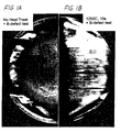
- a wafer from the ingot was separated into two sections after which one section was subjected to a B-defect annihilation process, wherein the section was heated to a temperature of about 1250 °C at a rate of about 25 °C, and maintained at that temperature for a hold time of about 10 seconds whereas the other section was not subjected to a B-defect annihilation process. Both sections were then treated with the B-defect delineating test discussed earlier and a digital image was taken of each delineated section. As shown in Figure 1, the wafer section subjected to the annihilation process (i.e.
- the section on the right in Figure 1 is substantially free of B-defects whereas the section of a wafer that was not subjected to the B-defect annihilation process (i.e., the section on the left in Figure 1) contains.B-defects, which appear as white dots in the center of the wafer.
- wafers were then cooled to room temperature.
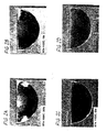
- wafer 1 shows a significant number of B-defects; when heated to 1100 °C for 15 seconds, wafer 2 shows considerably less B-defects; and when heated to 1100 °C for 60 seconds, wafer 3 shows almost no B-defects. (See Figure 2.)
- wafers 1 through 3 as the target temperature is increased to above 1100 °C, the B-defects are significantly reduced, and given a sufficient hold time, are almost completely eliminated.
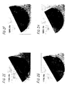
- the B-defects may be annihilated when heated to temperatures above 1150, 1175, 1200 and 1250 and held for time periods ranging from about 10 to about 60 seconds. (See Table 1 and Figures 2(e) through 2(1).)
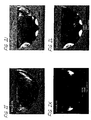
- Wafer 4 was treated according to an ideal precipitating wafer process wherein the temperature was increased at a rate of about 25 °C/min, the target temperature was about 1250 °C, the hold time was about 10 seconds, and the cool down rate was about 10 °C/min. While wafer 4 shows a significant number of white dots when subjected to the copper decoration method as shown in Figure 2(d), it is believed that the ideal precipitation sites were decorated by the copper decoration method and appear as white dots, such that even though the B-defects were annihilated in the process, the image of wafer 4 still shows white dots across the surface of the wafer.
- wafers 8 through 12 were subjected to the same temperature and hold time as wafer 4, however either the ambient or the cool down rate was varied such that the ideal precipitation sites were not formed. Wafers 8 through 12 show that B-defects are annihilated when a wafer is heated at a rate of about 25 °C/min to a temperature of about 1250 °C and held there for about 10 seconds, thus supporting the assumption that the white dots shown in wafer 4 are actually decorated ideal precipitation sites.
Landscapes
- Chemical & Material Sciences (AREA)
- Engineering & Computer Science (AREA)
- Crystallography & Structural Chemistry (AREA)
- Materials Engineering (AREA)
- Metallurgy (AREA)
- Organic Chemistry (AREA)
- Physics & Mathematics (AREA)
- Thermal Sciences (AREA)
- Crystals, And After-Treatments Of Crystals (AREA)
Applications Claiming Priority (5)
| Application Number | Priority Date | Filing Date | Title |
|---|---|---|---|
| US15572599P | 1999-09-23 | 1999-09-23 | |
| US155725P | 1999-09-23 | ||
| US17547800P | 2000-01-11 | 2000-01-11 | |
| US175478P | 2000-01-11 | ||
| PCT/US2000/025524 WO2001021865A1 (en) | 1999-09-23 | 2000-09-18 | Method for producing czochralski silicon free of agglomerated self-interstitial defects |
Publications (2)
| Publication Number | Publication Date |
|---|---|
| EP1222325A1 EP1222325A1 (en) | 2002-07-17 |
| EP1222325B1 true EP1222325B1 (en) | 2005-04-27 |
Family
ID=26852564
Family Applications (1)
| Application Number | Title | Priority Date | Filing Date |
|---|---|---|---|
| EP00961957A Expired - Lifetime EP1222325B1 (en) | 1999-09-23 | 2000-09-18 | Method for producing czochralski silicon free of agglomerated self-interstitial defects |
Country Status (7)
| Country | Link |
|---|---|
| US (1) | US6635587B1 (ko) |
| EP (1) | EP1222325B1 (ko) |
| JP (1) | JP4360770B2 (ko) |
| KR (1) | KR100778194B1 (ko) |
| DE (1) | DE60019780T2 (ko) |
| TW (1) | TW574449B (ko) |
| WO (1) | WO2001021865A1 (ko) |
Families Citing this family (9)
| Publication number | Priority date | Publication date | Assignee | Title |
|---|---|---|---|---|
| US7160385B2 (en) * | 2003-02-20 | 2007-01-09 | Sumitomo Mitsubishi Silicon Corporation | Silicon wafer and method for manufacturing the same |
| US6858307B2 (en) | 2000-11-03 | 2005-02-22 | Memc Electronic Materials, Inc. | Method for the production of low defect density silicon |
| US7105050B2 (en) | 2000-11-03 | 2006-09-12 | Memc Electronic Materials, Inc. | Method for the production of low defect density silicon |
| US6846539B2 (en) | 2001-01-26 | 2005-01-25 | Memc Electronic Materials, Inc. | Low defect density silicon having a vacancy-dominated core substantially free of oxidation induced stacking faults |
| CN1327041C (zh) | 2002-11-12 | 2007-07-18 | Memc电子材料有限公司 | 用于生长单晶锭的拉晶机和方法 |
| DE102007020006A1 (de) * | 2007-04-27 | 2008-10-30 | Freiberger Compound Materials Gmbh | Vorrichtung und Verfahren zur Herstellung von poly- oder multikristallinem Silizium, dadurch hergestellter Masseblock (Ingot) sowie Wafer aus poly- oder multikristallinem Silizium, und Verwendung zur Herstellung von Solarzellen |
| KR101168655B1 (ko) * | 2007-12-28 | 2012-07-25 | 삼성코닝정밀소재 주식회사 | N 타입 질화갈륨 웨이퍼의 광학 특성 향상 방법 |
| FR3034108A1 (fr) | 2015-03-24 | 2016-09-30 | Soitec Silicon On Insulator | Methode de reduction de defauts et fabrication de substrat |
| EP3346505A4 (en) | 2016-11-14 | 2019-01-16 | Shin-Etsu Chemical Co., Ltd | METHOD FOR THE PRODUCTION OF A SOLAR CELL HIGH PHOTOELECTRIC CONVERSION EFFICIENCY AND SOLAR CELL HIGH PHOTOELECTRIC CONVERSION EFFICIENCY |
Family Cites Families (51)
| Publication number | Priority date | Publication date | Assignee | Title |
|---|---|---|---|---|
| JPS583375B2 (ja) | 1979-01-19 | 1983-01-21 | 超エル・エス・アイ技術研究組合 | シリコン単結晶ウエハ−の製造方法 |
| FR2460479A1 (fr) * | 1979-06-29 | 1981-01-23 | Ibm France | Procede de caracterisation de la teneur en oxygene des barreaux de silicium tires selon la methode czochralski |
| US4266986A (en) * | 1979-11-29 | 1981-05-12 | Bell Telephone Laboratories, Incorporated | Passivation of defects in laser annealed semiconductors |
| JPS5680139A (en) | 1979-12-05 | 1981-07-01 | Chiyou Lsi Gijutsu Kenkyu Kumiai | Manufacture of semiconductor device |
| US4437922A (en) | 1982-03-26 | 1984-03-20 | International Business Machines Corporation | Method for tailoring oxygen precipitate particle density and distribution silicon wafers |
| JPS59124136A (ja) * | 1982-12-28 | 1984-07-18 | Toshiba Corp | 半導体ウエハの処理方法 |
| US4548654A (en) | 1983-06-03 | 1985-10-22 | Motorola, Inc. | Surface denuding of silicon wafer |
| US4505759A (en) | 1983-12-19 | 1985-03-19 | Mara William C O | Method for making a conductive silicon substrate by heat treatment of oxygenated and lightly doped silicon single crystals |
| US4851358A (en) | 1988-02-11 | 1989-07-25 | Dns Electronic Materials, Inc. | Semiconductor wafer fabrication with improved control of internal gettering sites using rapid thermal annealing |
| US4868133A (en) | 1988-02-11 | 1989-09-19 | Dns Electronic Materials, Inc. | Semiconductor wafer fabrication with improved control of internal gettering sites using RTA |
| US5264189A (en) | 1988-02-23 | 1993-11-23 | Mitsubishi Materials Corporation | Apparatus for growing silicon crystals |
| US4981549A (en) | 1988-02-23 | 1991-01-01 | Mitsubishi Kinzoku Kabushiki Kaisha | Method and apparatus for growing silicon crystals |
| US4929564A (en) * | 1988-10-21 | 1990-05-29 | Nippon Mining Co., Ltd. | Method for producing compound semiconductor single crystals and method for producing compound semiconductor devices |
| JPH039078A (ja) | 1989-06-05 | 1991-01-16 | Komatsu Ltd | 斜板式ピストンモータ |
| IT1242014B (it) | 1990-11-15 | 1994-02-02 | Memc Electronic Materials | Procedimento per il trattamento di fette di silicio per ottenere in esse profili di precipitazione controllati per la produzione di componenti elettronici. |
| JP2613498B2 (ja) | 1991-03-15 | 1997-05-28 | 信越半導体株式会社 | Si単結晶ウエーハの熱処理方法 |
| JP2758093B2 (ja) | 1991-10-07 | 1998-05-25 | 信越半導体株式会社 | 半導体ウェーハの製造方法 |
| JP3009078B2 (ja) | 1992-01-06 | 2000-02-14 | オムロン株式会社 | 文字認識装置 |
| JPH0684925A (ja) | 1992-07-17 | 1994-03-25 | Toshiba Corp | 半導体基板およびその処理方法 |
| KR0139730B1 (ko) | 1993-02-23 | 1998-06-01 | 사또오 후미오 | 반도체 기판 및 그 제조방법 |
| US5401669A (en) | 1993-05-13 | 1995-03-28 | Memc Electronic Materials, Spa | Process for the preparation of silicon wafers having controlled distribution of oxygen precipitate nucleation centers |
| JPH0786289A (ja) | 1993-07-22 | 1995-03-31 | Toshiba Corp | 半導体シリコンウェハおよびその製造方法 |
| IT1280041B1 (it) | 1993-12-16 | 1997-12-29 | Wacker Chemitronic | Procedimento per il tiraggio di un monocristallo di silicio |
| JP2725586B2 (ja) | 1993-12-30 | 1998-03-11 | 日本電気株式会社 | シリコン基板の製造方法 |
| JPH07249591A (ja) * | 1994-03-14 | 1995-09-26 | Matsushita Electric Ind Co Ltd | 半導体薄膜のレーザーアニール方法及び薄膜半導体素子 |
| JP2874834B2 (ja) | 1994-07-29 | 1999-03-24 | 三菱マテリアル株式会社 | シリコンウェーハのイントリンシックゲッタリング処理法 |
| JP3285111B2 (ja) | 1994-12-05 | 2002-05-27 | 信越半導体株式会社 | 結晶欠陥の少ないシリコン単結晶の製造方法 |
| US5611855A (en) | 1995-01-31 | 1997-03-18 | Seh America, Inc. | Method for manufacturing a calibration wafer having a microdefect-free layer of a precisely predetermined depth |
| JP3542189B2 (ja) * | 1995-03-08 | 2004-07-14 | 株式会社ルネサステクノロジ | 半導体装置の製造方法及び半導体装置 |
| US5788763A (en) | 1995-03-09 | 1998-08-04 | Toshiba Ceramics Co., Ltd. | Manufacturing method of a silicon wafer having a controlled BMD concentration |
| US5593494A (en) | 1995-03-14 | 1997-01-14 | Memc Electronic Materials, Inc. | Precision controlled precipitation of oxygen in silicon |
| JP3085146B2 (ja) | 1995-05-31 | 2000-09-04 | 住友金属工業株式会社 | シリコン単結晶ウェーハおよびその製造方法 |
| JPH08337490A (ja) | 1995-06-09 | 1996-12-24 | Shin Etsu Handotai Co Ltd | 結晶欠陥の少ないシリコン単結晶及びその製造方法 |
| JP3006669B2 (ja) | 1995-06-20 | 2000-02-07 | 信越半導体株式会社 | 結晶欠陥の均一なシリコン単結晶の製造方法およびその製造装置 |
| JP3381816B2 (ja) | 1996-01-17 | 2003-03-04 | 三菱住友シリコン株式会社 | 半導体基板の製造方法 |
| DE19637182A1 (de) | 1996-09-12 | 1998-03-19 | Wacker Siltronic Halbleitermat | Verfahren zur Herstellung von Halbleiterscheiben aus Silicium mit geringer Defektdichte |
| JPH10152395A (ja) | 1996-11-21 | 1998-06-09 | Komatsu Electron Metals Co Ltd | シリコン単結晶の製造方法 |
| KR100240023B1 (ko) | 1996-11-29 | 2000-01-15 | 윤종용 | 반도체 웨이퍼 열처리방법 및 이에 따라 형성된 반도체 웨이퍼 |
| KR100237829B1 (ko) | 1997-02-06 | 2000-01-15 | 윤종용 | 웨이퍼의 결함 분석방법 |
| US6045610A (en) | 1997-02-13 | 2000-04-04 | Samsung Electronics Co., Ltd. | Methods of manufacturing monocrystalline silicon ingots and wafers by controlling pull rate profiles in a hot zone furnance |
| US5994761A (en) | 1997-02-26 | 1999-11-30 | Memc Electronic Materials Spa | Ideal oxygen precipitating silicon wafers and oxygen out-diffusion-less process therefor |
| DE19711922A1 (de) | 1997-03-21 | 1998-09-24 | Wacker Siltronic Halbleitermat | Vorrichtung und Verfahren zum Ziehen eines Einkristalls |
| MY120036A (en) | 1997-04-09 | 2005-08-30 | Memc Electronic Materials | Low defect density, self- interstitial dominated silicon. |
| WO1998045507A1 (en) | 1997-04-09 | 1998-10-15 | Memc Electronic Materials, Inc. | Low defect density, ideal oxygen precipitating silicon |
| JPH1179889A (ja) | 1997-07-09 | 1999-03-23 | Shin Etsu Handotai Co Ltd | 結晶欠陥が少ないシリコン単結晶の製造方法、製造装置並びにこの方法、装置で製造されたシリコン単結晶とシリコンウエーハ |
| JP3144631B2 (ja) | 1997-08-08 | 2001-03-12 | 住友金属工業株式会社 | シリコン半導体基板の熱処理方法 |
| TW429478B (en) | 1997-08-29 | 2001-04-11 | Toshiba Corp | Semiconductor device and method for manufacturing the same |
| JPH11150119A (ja) | 1997-11-14 | 1999-06-02 | Sumitomo Sitix Corp | シリコン半導体基板の熱処理方法とその装置 |
| DE69933681T2 (de) | 1998-08-05 | 2007-08-23 | Memc Electronic Materials, Inc. | Ungleichmässige verteilung von minoritätsträger-lebensdauern in silizium-hochleistungsbauelementen |
| JP2002524845A (ja) | 1998-09-02 | 2002-08-06 | エムイーエムシー・エレクトロニック・マテリアルズ・インコーポレイテッド | 欠陥密度が低い単結晶シリコンから得られるシリコン・オン・インシュレーター構造体 |
| US6284384B1 (en) | 1998-12-09 | 2001-09-04 | Memc Electronic Materials, Inc. | Epitaxial silicon wafer with intrinsic gettering |
-
2000
- 2000-09-14 US US09/661,821 patent/US6635587B1/en not_active Expired - Fee Related
- 2000-09-18 KR KR1020027003800A patent/KR100778194B1/ko not_active IP Right Cessation
- 2000-09-18 WO PCT/US2000/025524 patent/WO2001021865A1/en active IP Right Grant
- 2000-09-18 JP JP2001525019A patent/JP4360770B2/ja not_active Expired - Fee Related
- 2000-09-18 DE DE60019780T patent/DE60019780T2/de not_active Expired - Lifetime
- 2000-09-18 EP EP00961957A patent/EP1222325B1/en not_active Expired - Lifetime
- 2000-10-12 TW TW89119618A patent/TW574449B/zh not_active IP Right Cessation
Also Published As
| Publication number | Publication date |
|---|---|
| KR100778194B1 (ko) | 2007-11-27 |
| EP1222325A1 (en) | 2002-07-17 |
| JP4360770B2 (ja) | 2009-11-11 |
| TW574449B (en) | 2004-02-01 |
| DE60019780T2 (de) | 2005-10-06 |
| JP2003510800A (ja) | 2003-03-18 |
| WO2001021865A1 (en) | 2001-03-29 |
| US6635587B1 (en) | 2003-10-21 |
| DE60019780D1 (de) | 2005-06-02 |
| KR20020042688A (ko) | 2002-06-05 |
Similar Documents
| Publication | Publication Date | Title |
|---|---|---|
| US6287380B1 (en) | Low defect density silicon | |
| US8216362B2 (en) | Controlling agglomerated point defect and oxygen cluster formation induced by the lateral surface of a silicon single crystal during CZ growth | |
| US20080020168A1 (en) | Silicon on insulator structure with a single crystal cz silicon device layer having a region which is free of agglomerated intrinsic point defects | |
| US6743289B2 (en) | Thermal annealing process for producing low defect density single crystal silicon | |
| US20050238905A1 (en) | Vacancy-dominated, defect-free silicon | |
| EP1222325B1 (en) | Method for producing czochralski silicon free of agglomerated self-interstitial defects | |
| EP1222324B1 (en) | Czochralski process for growing single crystal silicon by controlling the cooling rate | |
| EP1713121A2 (en) | Silicon on insulator structure from low defect density single crystal silicon |
Legal Events
| Date | Code | Title | Description |
|---|---|---|---|
| PUAI | Public reference made under article 153(3) epc to a published international application that has entered the european phase |
Free format text: ORIGINAL CODE: 0009012 |
|
| 17P | Request for examination filed |
Effective date: 20020423 |
|
| AK | Designated contracting states |
Kind code of ref document: A1 Designated state(s): AT BE CH CY DE DK ES FI FR GB GR IE IT LI LU MC NL PT SE |
|
| 17Q | First examination report despatched |
Effective date: 20030108 |
|
| RBV | Designated contracting states (corrected) |
Designated state(s): AT BE CH CY DE FR GB IT LI |
|
| GRAP | Despatch of communication of intention to grant a patent |
Free format text: ORIGINAL CODE: EPIDOSNIGR1 |
|
| RBV | Designated contracting states (corrected) |
Designated state(s): DE FR GB IT |
|
| GRAS | Grant fee paid |
Free format text: ORIGINAL CODE: EPIDOSNIGR3 |
|
| GRAA | (expected) grant |
Free format text: ORIGINAL CODE: 0009210 |
|
| AK | Designated contracting states |
Kind code of ref document: B1 Designated state(s): DE FR GB IT |
|
| REG | Reference to a national code |
Ref country code: GB Ref legal event code: FG4D |
|
| REG | Reference to a national code |
Ref country code: IE Ref legal event code: FG4D |
|
| REF | Corresponds to: |
Ref document number: 60019780 Country of ref document: DE Date of ref document: 20050602 Kind code of ref document: P |
|
| PLBE | No opposition filed within time limit |
Free format text: ORIGINAL CODE: 0009261 |
|
| STAA | Information on the status of an ep patent application or granted ep patent |
Free format text: STATUS: NO OPPOSITION FILED WITHIN TIME LIMIT |
|
| ET | Fr: translation filed | ||
| 26N | No opposition filed |
Effective date: 20060130 |
|
| PGFP | Annual fee paid to national office [announced via postgrant information from national office to epo] |
Ref country code: GB Payment date: 20110926 Year of fee payment: 12 |
|
| PGFP | Annual fee paid to national office [announced via postgrant information from national office to epo] |
Ref country code: IT Payment date: 20110927 Year of fee payment: 12 |
|
| GBPC | Gb: european patent ceased through non-payment of renewal fee |
Effective date: 20120918 |
|
| PG25 | Lapsed in a contracting state [announced via postgrant information from national office to epo] |
Ref country code: GB Free format text: LAPSE BECAUSE OF NON-PAYMENT OF DUE FEES Effective date: 20120918 |
|
| PG25 | Lapsed in a contracting state [announced via postgrant information from national office to epo] |
Ref country code: IT Free format text: LAPSE BECAUSE OF NON-PAYMENT OF DUE FEES Effective date: 20120918 |
|
| PGFP | Annual fee paid to national office [announced via postgrant information from national office to epo] |
Ref country code: DE Payment date: 20130927 Year of fee payment: 14 |
|
| PGFP | Annual fee paid to national office [announced via postgrant information from national office to epo] |
Ref country code: FR Payment date: 20130919 Year of fee payment: 14 |
|
| REG | Reference to a national code |
Ref country code: DE Ref legal event code: R119 Ref document number: 60019780 Country of ref document: DE |
|
| REG | Reference to a national code |
Ref country code: DE Ref legal event code: R119 Ref document number: 60019780 Country of ref document: DE Effective date: 20150401 |
|
| REG | Reference to a national code |
Ref country code: FR Ref legal event code: ST Effective date: 20150529 |
|
| PG25 | Lapsed in a contracting state [announced via postgrant information from national office to epo] |
Ref country code: DE Free format text: LAPSE BECAUSE OF NON-PAYMENT OF DUE FEES Effective date: 20150401 |
|
| PG25 | Lapsed in a contracting state [announced via postgrant information from national office to epo] |
Ref country code: FR Free format text: LAPSE BECAUSE OF NON-PAYMENT OF DUE FEES Effective date: 20140930 |