EP1195884A2 - Elektrische Energie(um)wandlungsvorrichtung - Google Patents
Elektrische Energie(um)wandlungsvorrichtung Download PDFInfo
- Publication number
- EP1195884A2 EP1195884A2 EP01106352A EP01106352A EP1195884A2 EP 1195884 A2 EP1195884 A2 EP 1195884A2 EP 01106352 A EP01106352 A EP 01106352A EP 01106352 A EP01106352 A EP 01106352A EP 1195884 A2 EP1195884 A2 EP 1195884A2
- Authority
- EP
- European Patent Office
- Prior art keywords
- bus bars
- input bus
- electric power
- plural number
- output bus
- Prior art date
- Legal status (The legal status is an assumption and is not a legal conclusion. Google has not performed a legal analysis and makes no representation as to the accuracy of the status listed.)
- Granted
Links
Images



Classifications
-
- H—ELECTRICITY
- H02—GENERATION; CONVERSION OR DISTRIBUTION OF ELECTRIC POWER
- H02M—APPARATUS FOR CONVERSION BETWEEN AC AND AC, BETWEEN AC AND DC, OR BETWEEN DC AND DC, AND FOR USE WITH MAINS OR SIMILAR POWER SUPPLY SYSTEMS; CONVERSION OF DC OR AC INPUT POWER INTO SURGE OUTPUT POWER; CONTROL OR REGULATION THEREOF
- H02M7/00—Conversion of AC power input into DC power output; Conversion of DC power input into AC power output
- H02M7/003—Constructional details, e.g. physical layout, assembly, wiring or busbar connections
-
- H—ELECTRICITY
- H10—SEMICONDUCTOR DEVICES; ELECTRIC SOLID-STATE DEVICES NOT OTHERWISE PROVIDED FOR
- H10W—GENERIC PACKAGES, INTERCONNECTIONS, CONNECTORS OR OTHER CONSTRUCTIONAL DETAILS OF DEVICES COVERED BY CLASS H10
- H10W44/00—Electrical arrangements for controlling or matching impedance
- H10W44/501—Inductive arrangements
-
- H—ELECTRICITY
- H10—SEMICONDUCTOR DEVICES; ELECTRIC SOLID-STATE DEVICES NOT OTHERWISE PROVIDED FOR
- H10W—GENERIC PACKAGES, INTERCONNECTIONS, CONNECTORS OR OTHER CONSTRUCTIONAL DETAILS OF DEVICES COVERED BY CLASS H10
- H10W72/00—Interconnections or connectors in packages
- H10W72/071—Connecting or disconnecting
- H10W72/073—Connecting or disconnecting of die-attach connectors
- H10W72/07351—Connecting or disconnecting of die-attach connectors characterised by changes in properties of the die-attach connectors during connecting
- H10W72/07354—Connecting or disconnecting of die-attach connectors characterised by changes in properties of the die-attach connectors during connecting changes in dispositions
-
- H—ELECTRICITY
- H10—SEMICONDUCTOR DEVICES; ELECTRIC SOLID-STATE DEVICES NOT OTHERWISE PROVIDED FOR
- H10W—GENERIC PACKAGES, INTERCONNECTIONS, CONNECTORS OR OTHER CONSTRUCTIONAL DETAILS OF DEVICES COVERED BY CLASS H10
- H10W72/00—Interconnections or connectors in packages
- H10W72/30—Die-attach connectors
- H10W72/341—Dispositions of die-attach connectors, e.g. layouts
- H10W72/347—Dispositions of multiple die-attach connectors
-
- H—ELECTRICITY
- H10—SEMICONDUCTOR DEVICES; ELECTRIC SOLID-STATE DEVICES NOT OTHERWISE PROVIDED FOR
- H10W—GENERIC PACKAGES, INTERCONNECTIONS, CONNECTORS OR OTHER CONSTRUCTIONAL DETAILS OF DEVICES COVERED BY CLASS H10
- H10W90/00—Package configurations
- H10W90/701—Package configurations characterised by the relative positions of pads or connectors relative to package parts
- H10W90/731—Package configurations characterised by the relative positions of pads or connectors relative to package parts of die-attach connectors
- H10W90/736—Package configurations characterised by the relative positions of pads or connectors relative to package parts of die-attach connectors between a chip and a stacked lead frame, conducting package substrate or heat sink
Definitions
- the present invention relates to an electric power conversion/inversion apparatus, such as, an inverter, etc., and in particular to an electric power conversion/inversion apparatus, being used as a motor driving apparatus for use in an automobile, upon which a high reliability is required.
- An inverter according to the conventional art 1, as was shown by a third embodiment in Japanese Patent Laying-Open No. Hei 11-346480 (1999), comprises: two power supply bus bars for inputting DC electric power from a DC power source and a capacitor; a plural number of output bus bars for outputting three-phase AC electric power to a motor; a plural number of semiconductor switching modules, being electrically connected to those power supply bus bars and the output bus bars, for inverting the DC electric power inputted into the three-phase AC electric power, to be outputted; and a heat sink on which are mounted those semiconductor switching modules, the power supply bus bars and the output bus bars.
- the plural number of the power supply bus bars comprises a positive (+) power supply bus bar and a negative (-) power supply bus bar.
- the plural number of the output bus bars is provided in number of three (3), so as to form three-phase thereby.
- the semiconductor module comprises three (3) parallel circuits, in each of which an IGBT and the reverse-parallel diode are connected, thereby forming each of the arms of a three-phase inverter.
- One of the phases of the three-phase bridge is formed with two (2) of the arms, and semiconductor modules constructing those two arms are provided on the heat sink through an insulator substrate, a common electrode pattern, and a high temperature soldering, so as to be disposed in parallel at both sides thereof.
- the output bus bars and the positive (+) power supply bus bar are provided on the heat sink, surrounding the semiconductor switching modules provided in parallel, through a insulator plate with contacting therewith.
- the negative (-) power supply bus bar is provided on the output bus bars through a insulator plate, with contacting therewith.
- the negative (-) power supply bus bar is disposed, so as to be located in a middle of the semiconductor switching modules provided in parallel. And, the output bus bars or the power supply bus bars and the semiconductor switching modules are connected therebetween through a wire bonding.
- the semiconductor switching modules forming an inverter main circuit and the bus bars are attached on the surface of the heat sink, to be contacted with, while a cooling water path is formed on the reverse surface thereof, to cool it, thereby obtaining small-sizing and a long life-time of the inverter apparatus for an electric car.
- the semiconductor apparatus having the semiconductor switching elements therein comprises: a pair of semiconductor switching elements, each having a positive electrode on one surface thereof while a negative one on the other surface; a circuit board, on which the pair of the semiconductor switching elements are mounted in different directions from each other, having a common land on which the positive electrode of one of the semiconductor switching elements and the negative electrode of the other semiconductor switching element are connected by soldering; and a wiring being positioned above the common land and extending in parallel thereto, on which the negative electrode of the one semiconductor switching elements and the positive electrode of the other semiconductor switching element are connected by soldering.
- the semiconductor apparatus according to this conventional art 2 is provided for the purpose of eliminating a wiring of a shape "L" therefrom, having a component or portion extending in an orthogonal direction to the substrate, thereby to prevent inductance and/or wiring resistance from being increased due to the same wiring in the orthogonal direction to the substrate, as well as obtaining small-sizing of a package by narrowing the distance between the semiconductor switching elements.
- the output bus bars and the positive (+) power supply bus bar are provided surrounding the semiconductor switching modules provided in parallel, while the negative (-) power supply bus bar in the middle of the semiconductor switching modules provided in parallel, therefore a plane space of the semiconductor apparatus as a whole comes to be a total of each plane area of the semiconductor switching modules, the output bus bars, and the positive (+) and the negative (-) power supply bus bars, or more.
- the semiconductor switching modules provided in parallel and the output bus bars which is provided therealong or the power supply bus bars are connected there between by the wire bonding, therefore the wiring as a whole comes to be complex, thereby increasing the circuit inductance and the wiring resistance thereof.
- the cooling of the semiconductor switching modules as a whole must be done by an amount of heat radiation through the heat sink on that one side thereof, therefore there is a problem that the heat radiation cannot be obtained with certainty.
- the semiconductor switching modules are provided on the common electrodes only through the soldering, and since, generally the semiconductor switching modules and the electrodes are different greatly in the linear expansion coefficient thereof, there is a problem that the soldering receives a large thermal fatigue from thermal cycles due to the intermittent ON-OFF operation of the semiconductor switching modules.
- An object, according to the present invention is to provide an electric power conversion/inversion apparatus, achieving reduction in the circuit inductance and the wiring resistance thereof, while bringing the apparatus to be compact in sized as a whole, thereby obtaining an electric conversion/inversion apparatus having a good installation, as well as a high reliability and an efficiency in the electric power conversion/inversion.
- Another object, according to the present invention is to provide an electric power conversion/inversion apparatus, achieving reduction in the circuit inductance and the wiring resistance thereof, and alsomitigating the thermal fatigue against the thermal cycles, while bringing the apparatus to be compact in sizes as a whole, thereby obtaining an electric conversion/inversion apparatus having a good installation, as well as a high reliability and an efficiency in the electric power conversion/inversion.
- an electric power conversion/inversion apparatus achieving reduction in the circuit inductance and the wiring resistance thereof, and also protecting the electrode surfaces of the semiconductor chips from deterioration due to elapse of time, while thereby obtaining an electric conversion/inversion apparatus having a good installation, as well as a high reliability and an efficiency in the electric power conversion/inversion.
- an electric power conversion/inversion apparatus comprising: a plural number of input bus bars for inputting electric power from an outside; a plural number of output bus bars for outputting electric power to the outside; and a plural number of semiconductor chips, being electrically connected to said input bus bars and said output bus bars for converting/inverting the electric power inputted into an output, wherein said plural number of input bus bars include a positive input bus bar and a negative input bus bar, being provided extending in parallel to each other, while said plural number of output bus bars are provided extending in parallel to each other and crossing over said positive and said negative input bus bars in longitudinal directions thereof, said plurality of semiconductor chips are disposed, being put between said positive input bus bar or said negative input bus bar and said plurality of output bus bars at crossing positions thereof, and connected electrically and thermally, to said positive input bus bar in a pole direction consistent therewith while to said negative input bus bar in a pole direction consistent therewith, and further to said common output
- said positive input bus bar and said negative input bus bar are elongated in a manner of a straight line and disposed in parallel to each other upon a same plane, while said output bus bars are elongated in a manner of a straight line and disposed in parallel to each other upon a same plane, so that said output bus bars cross over said positive and said negative input bus bars at about right angles, in the longitudinal directions thereof.
- said positive input bus bar and said negative input bus bar are connected to a positive input terminal and a negative input terminal, being formed in a laminated manner, from a side being same in the longitudinal direction thereof, respectively, while said plural number of output bus bars are connected to output terminals, respectively, from a side being same thereto but different from that of the positive and the negative input terminals, in the longitudinal direction thereof.
- said semiconductor chips each one being constructed with a MOSFET having a semiconductor switching element and a diode connected thereto in reverse-parallel direction, are connected between said input bus bars and said output bus bars, while said output bus bars being formed three in number, so that said semiconductor chips form a three-phase bridge, thereby inverting DC electric power inputted into three-phase AC electric power.
- an electric power conversion/inversion apparatus comprising: a plural number of input bus bars for inputting electric power from an outside; a plural number of output bus bars for outputting electric power to the outside; and a plural number of semiconductor chip carriers, being electrically connected to said input bus bars and said output bus bars for converting/inverting the electric power inputted into an output, wherein said plural number of input bus bars include a positive input bus bar and a negative input bus bar, being provided extending in parallel to each other, while said plural number of output bus bars are provided extending in parallel to each other and crossing over said positive and said negative input bus bars in longitudinal directions thereof, said plurality of semiconductor chip carriers, each having a semiconductor chip including a semiconductor switching element therein and a metal member being electrically and thermally connected to a positive surface and a negative surface on both sides of said semiconductor chip, are disposed, being put between said positive input bus bar or said negative input bus bar and said plurality of output bus bars at
- said metal member is formed of a low thermal expansion metal material having a low linear thermal expansion coefficient being near to that of said semiconductor chip, and is connected to said semiconductor chip through a bonding material.
- said metal member is formed of a low thermal expansion metal material having a low linear thermal expansion coefficient within a range from 3 to 10.
- a projection portion and an engagement portion of said semiconductor chip carrier and said input bus bar or said output bus bar are engaged, thereby providing a positioning mechanism for fixing both positions.
- said metal member has an area being larger than that of a projection area of said semiconductor chip, and a thickness thereof is thin, around from 1 mm to 2 mm in thickness thereof.
- an electric power conversion/inversion apparatus comprising: a plural number of input bus bars for inputting electric power from an outside; a plural number of output bus bars for outputting electric power to the outside; a plural number of semiconductor chip carriers, being electrically connected to said input bus bars and said output bus bars for converting/inverting the electric power inputted into an output; and a suppression mechanism for suppressing said input bus bars and said output bus bars onto said semiconductor chip carriers, wherein said plural number of input bus bars include a positive input bus bar and a negative input bus bar, being provided extending in parallel to each other, while said plural number of output bus bars are provided extending in parallel to each other and crossing over said positive and said negative input bus bars in longitudinal directions thereof, said plurality of semiconductor chip carriers, each having a semiconductor chip including a semiconductor switching element therein and a low thermal expansion metal member being electrically and thermally connected to a positive surface and a negative surface on both sides of said semiconductor chip, are
- a ratio between a width and a thickness of said input bus bar is set within a range from 5 to 10.
- an electric power conversion/inversion apparatus comprising: a plural number of input bus bars for inputting electric power from an outside; a plural number of output bus bars for outputting electric power to the outside; a plural number of semiconductor chip carriers, being electrically connected to said input bus bars and said output bus bars for converting/inverting the electric power inputted into an output; a case for having said and semiconductor chip carriers built-in; and a cooler for cooling said plural number of input bus bars or said plural number of output bus bars, wherein said plural number of input bus bars and said plural number of output bus bars are provided so that they intersect to each other, said plurality of semiconductor chip carriers, each having a semiconductor chip including a semiconductor switching element therein and a metal member being electrically and thermally connected to a positive and a negative surfaces on both sides of said semiconductor chip, are disposed to be put between said input bus bars and said plurality of output bus bars, at crossing positions thereof, being connected electrically and thermally,
- suppression mechanisms are provided onto said input bus bars or said output bus bars, which are molded with said case in one body, so as to suppress said output bus bars or said input bus bars.
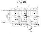
- FIG. 23 is a circuit diagram for showing the electric conversion/inversion apparatus in a motor driver system for use in an automobile.
- DC current from a battery 303 is changed or inverted into AC current through an inverter circuit 306, being variable in voltage and frequency thereof, so as to control an AC three-phase electric rotating machine 305.
- Battery voltage in the present embodiment is set to around 42V obtained by connecting batteries in series, for example, in number of three (3), each having an output of 14V and is widely and commonly used in a car, by taking the fact that endurance voltage of a semiconductor chip 1 constructed with MOSFET (Metal Oxide Semiconductor Field Effect Transistor) is around 100V at the maximum into the consideration.
- MOSFET Metal Oxide Semiconductor Field Effect Transistor
- a main circuit of the inverter circuit 306 is constructed with three (3) sets of circuits, 301u, 301v and 301w, each generating an output of one phase of the three-phase AC current, being connected in parallel to a DC input.
- suffixes "u” , “v” and “w” are attached after the reference numerals or marks for the purpose of distinction among the three (3) phases thereof, however there are cases where those suffixes "u”, “v” and “w” are omitted, in particular when they are indicated commonly or representatively, in the explanation given below.
- a circuit 301 for one (1) phase is constructed with a positive semiconductor chip 1p for generating an output of a plus side with respect to a reference electrical potential and a negative semiconductor chip In for generating an output of a minus side, being connected in series as one set, thereby changing DC current inputted into pulses having three levels, i.e., a positive one, a negative one and a neutral one.
- suffixes "p" and “n” are attached after the reference numerals or marks for the purpose of distinction between the positive and the negative thereof, however there are cases where those suffixes "p” and "n” are omitted, in particular when they are indicated commonly or representatively, in the explanation given below.
- the electrical rotating machine 305 herein, is used as an electric motor for use in an automobile.
- this electrical rotating machine 305 is to be operated as the electric motor, the three-phase AC current of variable voltage and frequency is inputted to it, thereby controlling the rotation thereof so as to generate motive power therefrom.
- the electrical rotating machine 305 so as to operate as a generator or a dynamo, and during regenerative operation, on the contrary to the operation mentioned above, energy generated thereby flows into the battery 303 to be charged therein.
- heat-generative electrical parts aremainly the semiconductor chips 1, and there is a necessity of protecting the semiconductor chips 1 from an increase of temperature by using a heat radiation means, so that the temperature does not exceed a heat-durable temperature of the semiconductor chip 1.
- thermal resistance of an inverter module, in which the semiconductor chips 1 are installed or mounted occupies a large part of ratio to a total thermal resistance. Therefore, the inverter module installing the semiconductor chips therein is required to be lowered in the thermal resistance in the structure thereof.
- the electric power conversion/inversion apparatus used in an automobile is mainly operated to supply electric energy at frequent, for the purpose of flowing large current in a short time period, for example, when supplying the electric energy so as to assist an engine generating a torque therefrom through the electrical rotating machine 305 in the short time period, and when supplying the electric energy so as to drive the engine through the electrical rotating machine 305 when it starts up by itself.
- the electric power conversion/inversion apparatus, and in particular the semiconductor chips 1 generating heat therefrom receives very severe thermal cycles. Therefore, it is necessary to protect the inverter module from thermal fatigue and breakdown thereof, due to the heat cycles given intermittently for a long time. For that reason, the module is required to be strong against the thermal cycles in the structure thereof.
- the endurance voltage of the semiconductor chip 1 is about 100V, in general, therefore it is only as two (2) times large as the battery voltage if it is set to 42V in the manner of the present embodiment. Under such the condition of use, when the circuit inductance is large, there is a possibility that the voltage jumping up when being switched comes up to be so large as to break down the semiconductor chip 1. Therefore, the inverter is required to have a low circuit inductance in the structure thereof.
- the present invention is made for satisfying such the requirements mentioned in the above.
- Fig. 1 is a cross-section view for showing the structure of an electric power conversion/inversion apparatus, according to a first embodiment of the present invention
- Fig. 2 is a cross-section view along A-A plane shown in the Fig. 1
- Fig. 3 is a cross-section view along B-B plane shown in the Fig. 1
- Fig. 4 is a cross-section view, being orthogonal to a lamination direction of a chip carrier 11 shown in the Fig. 2
- Fig. 5 is a cross-section view along C-C plane shown in the Fig. 4;
- Fig. 1 is a cross-section view for showing the structure of an electric power conversion/inversion apparatus, according to a first embodiment of the present invention
- Fig. 2 is a cross-section view along A-A plane shown in the Fig. 1
- Fig. 3 is a cross-section view along B-B plane shown in the Fig. 1
- Fig. 4 is a cross-section view, being orthogonal to
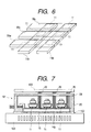
- Fig. 6 is a perspective view of main circuit wirings and the chip carriers being extracted from, in the first embodiment according to the present invention.
- Fig. 7 is a view of the construction of the electric power conversion/inversion apparatus and peripheral equipments thereof, according to the first embodiment of the present invention, respectively.
- the chip carrier 11 is constructed to have the semiconductor chip 1 and metal members 3s and 3d having low thermal expansion, being bonded through bonding members (for example, solder, etc.) 2s and 2d on the surfaces of both sides thereof.
- bonding members for example, solder, etc.
- an upper surface of the semiconductor chip 1 is an electrode surface on a source side, while a lower surface is an electrode surface on a drain side thereof.
- a suffix "s" is attached after a member located on the source side while “d” after a member located on the drain side, however there are cases where they are omitted, in particular when they are indicated commonly or representatively, in the explanation given hereinafter.
- the low thermal expansion metal means a metal having a small coefficient of linear thermal expansion, being same or similar to that of silicon (about 3), which is used as a material of the semiconductor chip 1, for example, molybdenum having the linear thermal expansion coefficient of about 5 or alloy of copper oxide having the linear thermal expansion coefficient of about 10 or the like can be used.
- a control terminal 4 for taking out a signal from a control electrode is electrically connected to the control electrode of the semiconductor chips 1 through a bonding member 2g of, such as, solder, etc.
- the main circuit current flows through the electrode surface on the drain side of the semiconductor chip 1, over a whole area thereof, the whole surface is connected to the low thermal expansion metal member 3d through the bonding member (for example, of solder, silver paste, etc.) 2d.
- the bonding member for example, of solder, silver paste, etc.
- the low thermal expansion metal member 3 is formed into such sizes, that it has an area larger than the projection area of the semiconductor chip 1 thereon. Also, with thickness thereof, it is preferably to be set from about 1mm to about 2mm, by taking into the consideration that the thermal resistance component comes to be too large in the vertical direction, comparing to the effect obtained as a thermal diffusion plate, if it is too thick, and that the low thermal expansion metal member 3 is, in general, made of an expensive material.
- two input bus bars 14p and 14n are disposed in parallel, extending in the longitudinal direction thereof along with each other.
- suffixes "p” and “n” are attached after the reference numerals or marks for the purpose of distinction between the positive and the negative, however there are cases where those suffixes "p” and “n” are omitted, in particular when they are indicated commonly or representatively in the explanation given below.
- Those input bus bars 14 are made of a material, such as copper or aluminum.
- a side surface of the positive input bus bar 14p, having no contact with the chip carrier 11, is disposed within a case 20 to be exposed from a lower surface thereof, functioning as a cooling surface, upon which the case is attached on the metal-made heat sink 103 (see Fig. 7) which constructs a cooler.
- the case 20 is made by mold forming of resin, etc., and is molded together with the positive input bus bar 14p and the negative input bus bar 14n as one or in one body; therefore they are fixed onto the base 20.
- cooling side surfaces of the positive input bus bar 14p and the negative input bus bar 14n are formed with an insulator layer 15 thereon, for the purpose of ensuring electric insulation, made of resin containing mainly epoxy, etc., or ceramic powder, for example.
- the positive input bus bar 14p and the negative input bus bar 14n are molded with the case 20 in one body, however in the construction thereof, the case 20 exposes not only the cooling surface upon which it contacts with the cooler 103 through the insulator layer 15, but also an upper surface thereof for contacting with the chip carrier 11.
- the heat sink 103 is attached, with contacting onto the cooling side surfaces of the positive input bus bar 14p and the negative input bus bar 14n, by using a fixing bore 25 opened in the module case 20 and a bolt not shown in the figure.
- thermal conductive grease 102 is put into an opening or aperture defined between the insulator layer 15 on the cooling side surfaces of the positive and negative input bus bars 14p and 14n and the heat sink 103.
- the output bus bars 18 are disposed on upper surfaces thereof, while being connected electrically. Those output bus bars 18 are disposed so that they intersect the input bus bars 14 at about right angles to each other, with respect to the longitudinal directions thereof. Such combinations of the chip carriers 11 are three (3) in the number thereof, in total, and the output bus bars 18 are disposed in a pair on each of the chip carriers 11.
- the suppression body 24 Onto the laminated layer structure of the chip carriers 11, input bus bars 14 and the output bus bars 18 mentioned above, as shown in Fig. 2, there is further laminated a suppression body 24 upon the upper surface of the output bus bars 18.
- the suppression body 24 has a bore in a center thereof, and into this bore is inserted a joint means (for example, a screw, etc.) 21 penetrating therethrough, wherein joining the joint means 21 into the female screw portion 22 which is provided within the case 20 molding the input bus bars 14 in one body.
- the chip carriers 11 are suppressed by means of the input bus bars 14 and the output bus bars 18 to be connected with, thereby obtaining the electrical and thermal connection between them with certainty.
- an insulator layer 19 and an elastic body 23, such as a disc spring, etc. for the purpose of protecting the suppression from abrupt decrease due to loosing of the screw 21, etc.
- the input bus bars 14p and 14n are, as apparent from Fig. 1, connected to a positive and a negative input terminals 12p and 12n which are formed with the case 20 in one body through wiring members 13p and 13n for use in connection.
- the positive and the negative input terminals 12p and 12n are located close to each other, so far as the insulation can be ensured on both wiring surfaces thereof, i.e., in a form of the laminated structure.
- the output bus bars 18u, 18v and 18w are connected to output terminals 16u, 16v and 16w, which are also formed with the case 20 in one body, through wiring members 17u, 17v and 17w.
- control terminals 4 to be taken out from each chip carrier 11 are connected to control wiring bodies 26 which are disposed on the case 20, and further through control terminal pins 27, which are formed on those wiring bodies 26, control signals are taken out upon the upper surfaces of the modules.
- control wiring bodies 26 which are disposed on the case 20, and further through control terminal pins 27, which are formed on those wiring bodies 26, control signals are taken out upon the upper surfaces of the modules.
- controller substrate 104 Above the upper surfaces of the modules is disposed a controller substrate 104 (see Fig. 7) in the vicinity thereof, and control pins 27 are connected thereto.
- the inverter circuit being applied into the present embodiment for taking out three-phase AC output from the DC power source having the positive and negative poles, is most simple in the structure thereof. Namely, the polarities of the chip carriers 11 which are mounted on the positive and the negative input bus bars 14p and 14n are made different to each other, and to those are electrically connected the AC output bus bars 18, thereby constructing the inverter circuit for one phase. Further, by disposing the output bus bars 18 so that the longitudinal direction thereof intersects at the about right angles with respect to longitudinal direction of the input bus bars, i.e., the direction in which the chip carriers 11 are aligned thereon, it is possible to dispose in the most compact form the output bus bars 18 for those three phases.
- this configuration can contribute, not only to small-sizing of the inverter module, but also enables a low inductance of the circuit as a whole, since no such a current component occurs at all other than the portions of the chip carriers 11 that intersects the input wiring at the right angles, but occurs necessarily when all the chip carriers 11 are installed in the same polarity, therefore there is no necessity of increasing up the endurance voltage for the elements more than the value required from a circuitry viewpoint. Also, the resistance of the semiconductor element must not be larger than the necessary value thereof, and this enables an improvement in an efficiency of electric power conversion/inversion as the basic performance of the inverter circuit.
- the chip carriers 11 are obtained by bonding onto the semiconductor chips 1 the low thermal expansion metal member 3, having the linear thermal expansion coefficient thereof. With this, it is possible to protect the solder bonding portion from the thermal fatigue and destruction due to the thermal cycles.
- the material for constructing the output bus bars 18 it is general to use a metal material, having a large linear thermal expansion coefficient (about 20) comparing to that of the semiconductor chip 1 and the low thermal expansion metal member 3, such as copper or aluminum, and in this instance, since the output bus bars 18 are pressingly contacted upon the surface of the low thermal expansion metal members 3 of the chip carriers 11, it is possible to protect the bonding portions from the fatigue and destruction caused due to inconsistency in the linear thermal expansion coefficient between the semiconductor chip 1 and the low thermal expansion metal member, and the output bus bars 18.
- the inverter module since it adopts the bonding structure, in which the low thermal expansion metal member 3 is bonded upon the electrode surfaces of the semiconductor chip 1, being basically most sensitive in contaminated circumferences, so as to cover them, it is possible to protect the electrode portions of the semiconductor chip 1 from the deterioration due to the elapse of time. With this, since there is no need of applying such the complete sealing structure that is necessary in the suppressive contact structure according to the conventional art, the inverter module can be more simplified in the structure thereof, and as a result enable to lower the costs .
- sealing material such as gel or resin
- the present mount structure is a one-side cooling structure, having the cooling surface only on one side, however the low thermal expansion metal member 3 and the output bus bars 18 performs the function as a thermal storage when conduction time is short, therefore it has a feature that transitional thermal resistance can be made small comparing to the normal one-side cooling structure.
- Such the feature functions effectively, in particular when it is applied into the control for, such as, an automobile appliance or a motor for use in an automobile, which is mainly used at rating thereof for a short time.
- two input bus bars 14p and 14n are used as the cooling surface, and this is because it is possible to ensure the width of them to be wider than the width of the bus bars obtainable when the three (3) output bus bars 18 are fixed totally in the direction of the width thereof as the cooling surface, and as a result of this, the thermal resistance can be reduced down much more.
- the contact thermal resistance between the chip carriers 11 and the input bus bars 14 there lies the contact thermal resistance between the chip carriers 11 and the input bus bars 14, however this contact thermal resistance can be reduced down to a degree corresponding to the solder layer of thickness around 0.1 mm, under a pressure within a limit of suppression upon the semiconductor 1.
- Fig. 9 results of the thermal resistances and the inductances, which are calculated out by making the ratio between the width of the input bus bar and the thickness as a parameter thereof, when setting the width of the input bus bar at a constant value.
- the vertical axis of this graph are indicated relative values, obtained through normalization of the respective values by allowable design values. According to this, the smaller the thickness of the input bus bar, the lower the inductance, however the thermal resistance shows a tendency of increasing up, thereby reducing the function as the heat or thermal diffusing plate.
- an appropriate range in the ratio of the bus bar lies preferably in the range from about 5 to about 20 in the ratio, between the width and the thickness of the input bus bar.
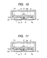
- Fig. 10 is a cross-section view for showing the structure of the electric power conversion/inversion apparatus, according to the second embodiment of the present invention.
- the elastic body 23, such as a disc spring, etc., is inserted between the bolt 21 and the output bus bar 18.
- the output bus bar 18 functions also as the suppression body by itself, in common, in place of the suppression body 24 that is necessary in the first embodiment, it is possible to achieve the suppressive contact structure being simplified in the structure thereof.
- Fig. 11 is a cross-section view for showing the structure of the electric power conversion/inversion apparatus, according to the third embodiment of the present invention.
- the elastic body 23 is eliminated in the second embodiment, and the output bus bar 18 serves both as the elastic body and as the suppression body, and as the output bus bar 18, as well, by itself, commonly in the construction thereof, thereby achieving the suppressive contact structure being simplified much more.
- the flexibility of the output bus bar 18 is utilized, it is preferable to treat flat surface finishing on both contacting surfaces of the chip carrier 11 and the output bus bar 18, by taking the change in parallelism between the two (2) plane surfaces due to that flexibility into the consideration.
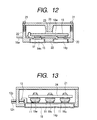
- Fig. 12 is a cross-section view for showing the structure of the electric power conversion/inversion apparatus, according to the fourth embodiment of the present invention.
- the chip carriers 11 are suppressed with using a case cover 28, and the case 20 and the case cover 28 are fixed between them by means of the joint means (such as, the bolt, etc.) 21.
- the joint means necessary for suppression can be shared by a sealing means for preventing the inverter module from being contaminated inside thereof, in common, it is possible to realize the inverter module, being superior in the characteristic of hostile-environment further more.
- the three (3) output bus bars 18 are suppressed by only one (1) case cover 28, it is possible to simplify the suppressing mechanism.
- FIG. 13 is a cross-section view for showing the structure of the electric power conversion/inversion apparatus, according to the fourth embodiment of the present invention.
- the suppression bodies 24 for suppressing each of the output bus bars 18 are integrated in one body, and further it is made of the material of a metal.
- the suppression body 24 comes to be a metal plate of covering the six (6) chip carriers 11 as a whole, so as to function as a shield against an electromagnetic wave generated when the semiconductor chip 1 is switched over, therefore it can achieve a roll of preventing the controller substrate 104 (see the Fig. 7), etc., which is provided in the vicinity of the inverter module, from mal function thereof.
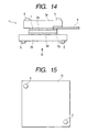
- the Fig. 14 is a cross-section view for showing the structure of the chip carrier in the electric power conversion/inversion apparatus, according to the sixth embodiment of the present invention.
- the Fig. 15 is a construction view seen in a direction D in the Fig. 14.
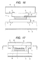
- Fig. 16 is a cross-section view of the construction combining the bus bars with the construction shown in the Fig. 14.
- a positioning mechanism is provided for the purpose of performing the positioning of the chip carriers 11 with high accuracy, when manufacturing the inverter module.
- Upon the contact surface of the chip carrier 11 are provided projection portions at least two (2) or more, while engagement portions (for example, openings, etc.) corresponding thereto on the sides of the bus bars 14 and 18.
- the positioning mechanism is preferable to be different in sizes and/or positions thereof, on both surfaces of the chip carrier 11. In more details, in order to disable mounting of the chip carrier 11 even if it is tried with being turned over in the polarity by mistake, or to detect the error with ease, it is desirable to make the distance between two (2) projections or the sizes thereof being different on both surfaces.
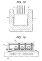
- the Fig. 17 is a cross-section view for showing the structure of a chip carrier portion in the electric power conversion/inversion apparatus, according to a seventh embodiment of the present invention.
- the Fig. 18 is a cross-section view along E-E cross-section shown in the Fig. 17.
- a pressure guide 7 is inserted between the chip carriers 11 and the output bus bars 18, so as to minimize the suppression force applied onto the semiconductor chips 1 comparing to the suppression force generated upon the contact surface between the chip carriers 11 and the input bus bars 18.
- FIG. 19 is a cross-section view for showing the structure of the electric power conversion/inversion apparatus, according to the eighth embodiment of the present invention.
- the input bus bars 14 without provision of the insulator layer upon the cooling surface of the input bus bars 14, but in place thereof are inserted the input bus bars 14 and an insulator seat 105 detachable between the heat sink 103.
- change in dielectric strength of insulation can be done easily by changing the endurance voltage of the elements, thereby obtaining an inverter module structure being common to the modules of elements, having different endurance voltages other than the MOSFET.
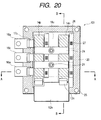
- the Fig. 20 is a cross-section view for showing the structure of the electric power conversion/inversion apparatus, according to the ninth embodiment of the present invention.
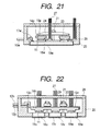
- the Fig. 21 is a cross-section view along A-A plane shown in the Fig. 20.
- the Fig. 22 is a cross-section view along B-B plane shown in the Fig. 20.
- the output bus bar 18 has the cooling surface thereon.
- the input bus bars 14, which gives large influence upon the inductance do not contribute to the cooling performance so much, therefore being providing the structure being suitable in a case where the inductance must be small further more.
- the semiconductor chips 1 are disposed to be put between the positive input bus bar 14p and the negative input bus bar 14n and the output bus bars 18, at crossing positions thereof, and are connected, electrically and thermally, to the positive input bus bar 14p in a pole direction consistent therewith while to the negative input bus bar 14n in a pole direction consistent therewith, and further to the common output bus bars 18 in pole directions being different from side by side, therefore, the neighboring semiconductor chips, the neighboring input bus bars 14 and the neighboring output bus bars 18 can be disposed in the vicinity thereof, respectively, so as to brig it to be very compact as a whole.
- the positive input bus bar 14p and the negative input bus bar 14n are connected to a positive input terminal 12p and a negative input terminal 12n, which are formed in a laminated manner, from the same side in the longitudinal direction thereof, respectively, while the output bus bars 18 are connected to output terminals 16, respectively, from a side being same thereto but different from that of the positive and the negative input terminals 12p and 12n, in the longitudinal direction thereof, therefore it is possible to enlarge a lamination area of the positive input terminal 12p and the negative input terminal 12n, by utilizing spaces between the positive input bus bar 14p and the negative input bus bar 14n, which are disposed in parallel without restriction due to the output terminals 16. With this, it is possible to obtain the reduction of the circuit inductance, further more.
- a semiconductor chip carrier 11 is constructed with the semiconductor chip 1 having a semiconductor-switching element therein and metal members 3 connected to a positive and a negative electrode surfaces on both sides of the semiconductor chip 1, and the semiconductor chips 1 are disposed to be put between the positive input bus bar 14p and the negative input bus bar 14n and the output bus bars 18, at crossing positions thereof, and are connected, electrically and thermally, to the positive input bus bar 14p in a pole direction consistent therewith while to the negative input bus bar 14n in a pole direction consistent therewith, and further to the common output bus bars 18 in pole directions being different from side by side, thereby obtaining the thermal and the electrical connection between the semiconductor chip 1 and the input and output bus bars 14 and 18 on both sides thereof through the metal members 3, at high efficiency and with certainty, while keeping a total body compact and the low circuit inductance and the low resistance, ensuring certainty and reliability in the operation of the semiconductor switching elements, and enabling a protection of the electrode surfaces of the semiconductor chip 1, being most sensitive to contamination from the elapse of time, by sealing them
- the metal member 3 is formed of a low thermal expansion metal material having a low linear thermal expansion coefficient being near to that of the semiconductor chip 1, and is connected to the semiconductor chip 1 through soldering 2 for use in connection, thereby constructing semiconductor chip carrier 11, therefore, the difference between the semiconductor chip 1 and the metal member 3 comes to be small in an amount of change in the thermal expansion thereof, thereby mitigate thermal fatigue applied onto soldering 2 for use in connection. With this, it is possible to protect the semiconductor chip carrier 11 from the destruction due to the thermal fatigue thereof.
- the metal member 3 has an area being larger than that of a projection area of the semiconductor chip, and a thickness thereof is thin, about from 1 mm to 2 mm in thickness thereof, therefore it is possible to diffuse heat generated from the semiconductor chip 1 widely in a direction of the plane thereof, and also to make small a use amount of the low thermal expansion metal material 3, which is high in a price in general.
- a suppression mechanism is provided for suppressing the input bus bars 14 and the output bus bars 18 onto the semiconductor chi carriers 11, therefore it is possible to connect the input bus bars 14 and the output bus bars 18 onto the semiconductor chi carriers 11, electrically and thermally, without through the connecting solder, etc., as well as, to dissolve problems due to the thermal fatigue of the connecting solder, thereby enabling to manufacture the apparatus easily and cheaply.
- the input bus bars 14 and the output bus bars 18 are molded with the case 20 in one body when it is formed of plastic, and the cooler 103 is connected thermally through the electrical insulating layer on the surface of the side opposing to the semiconductor chip carriers 11 (i.e., an unti- semiconductor chip carrier side), on which the input bus bars 14 or the output bus bars 18 are exposed, therefore it is possible to protect the semiconductor chip carriers 11 from the contamination due to dust of anoutside thereof, and at the same time, to cool the semiconductor chip carriers 11 within the case 20 through the input bus bars 14 or the output bus bars 18, with certainty, and to ensure the reliability of the semiconductor chip carriers 11.
- the semiconductor chip carriers 11 i.e., an unti- semiconductor chip carrier side
- the input bus bars 14 or the output bus bars 18, which are formed with the case 20 in one body, constitutes a suppressing mechanism for suppressing the output bus bars 18 or the input bus bars 14 provided on the opposing side thereof, therefore obtaining the suppression with a simple structure.
- the electric power conversion/inversion apparatus achieving reduction in the circuit inductance and the wiring resistance thereof, while bringing the apparatus to be compact in sized as a whole, thereby accomplishing the electric conversion/inversion apparatus having a good installation, as well as a high reliability and an efficiency in the electric power conversion/inversion.
- the electric power conversion/inversion apparatus obtaining reduction in the circuit inductance and the wiring resistance thereof, and also mitigation of the thermal fatigue against the thermal cycle, while bringing the apparatus to be compact in sized as a whole, thereby accomplishing the electric conversion/inversion apparatus having a good installation, as well as a high reliability and a high efficiency in the electric power conversion/inversion.
- the electric power conversion/inversion apparatus obtaining reduction in the circuit inductance and the wiring resistance thereof, and also protection of the electrode surfaces of the semiconductor chips from deterioration due to elapse of time, while bringing the apparatus to be compact in sized as a whole, thereby accomplishing an electric conversion/inversion apparatus having a good installation, as well as a high reliability and a high efficiency in the electric power conversion/inversion.
Landscapes
- Engineering & Computer Science (AREA)
- Power Engineering (AREA)
- Inverter Devices (AREA)
- Power Conversion In General (AREA)
Applications Claiming Priority (2)
| Application Number | Priority Date | Filing Date | Title |
|---|---|---|---|
| JP2000283004 | 2000-09-19 | ||
| JP2000283004A JP3793407B2 (ja) | 2000-09-19 | 2000-09-19 | 電力変換装置 |
Publications (3)
| Publication Number | Publication Date |
|---|---|
| EP1195884A2 true EP1195884A2 (de) | 2002-04-10 |
| EP1195884A3 EP1195884A3 (de) | 2004-02-25 |
| EP1195884B1 EP1195884B1 (de) | 2006-05-24 |
Family
ID=18767425
Family Applications (1)
| Application Number | Title | Priority Date | Filing Date |
|---|---|---|---|
| EP01106352A Expired - Lifetime EP1195884B1 (de) | 2000-09-19 | 2001-03-16 | Elektrische Energie(um)wandlungsvorrichtung |
Country Status (4)
| Country | Link |
|---|---|
| US (1) | US6618278B2 (de) |
| EP (1) | EP1195884B1 (de) |
| JP (1) | JP3793407B2 (de) |
| DE (1) | DE60119865T2 (de) |
Cited By (3)
| Publication number | Priority date | Publication date | Assignee | Title |
|---|---|---|---|---|
| EP1576718A1 (de) * | 2002-12-23 | 2005-09-21 | Danaher Motion Stockholm AB | Motorantriebseinheit typ wechselrichter |
| EP1855374A2 (de) | 2006-04-27 | 2007-11-14 | Hitachi, Ltd. | Stromkreisvorrichtung, Stromkreismodul und Stromwandler |
| US11063495B2 (en) | 2019-07-01 | 2021-07-13 | Nidec Motor Corporation | Heatsink clamp for multiple electronic components |
Families Citing this family (89)
| Publication number | Priority date | Publication date | Assignee | Title |
|---|---|---|---|---|
| US20030218057A1 (en) * | 2000-11-07 | 2003-11-27 | Craig Joseph | Electrical bus with associated porous metal heat sink and method of manufacturing same |
| US6678182B2 (en) * | 2000-11-07 | 2004-01-13 | United Defense Lp | Electrical bus with associated porous metal heat sink and method of manufacturing same |
| JP4540884B2 (ja) * | 2001-06-19 | 2010-09-08 | 三菱電機株式会社 | 半導体装置 |
| JP3641232B2 (ja) * | 2001-11-13 | 2005-04-20 | 本田技研工業株式会社 | インバータ装置及びその製造方法 |
| US7068507B2 (en) * | 2002-09-27 | 2006-06-27 | Rockwell Automation Technologies, Inc. | Compact liquid converter assembly |
| US6822850B2 (en) * | 2002-09-27 | 2004-11-23 | Rockwell Automation Technologies, Inc. | Laminated bus bar for use with a power conversion configuration |
| US20040060689A1 (en) * | 2002-09-27 | 2004-04-01 | Pfeifer David W. | Compact liquid cooled heat sink |
| US6956742B2 (en) * | 2002-09-27 | 2005-10-18 | Rockwell Automation Technologies, Inc. | Compact liquid converter assembly |
| US6885553B2 (en) * | 2002-09-27 | 2005-04-26 | Rockwell Automation Technologies, Inc. | Bus bar assembly for use with a compact power conversion assembly |
| GB0226714D0 (en) * | 2002-11-15 | 2002-12-24 | Bombardier Transp Gmbh | Converter module |
| US20040165015A1 (en) * | 2003-02-20 | 2004-08-26 | Blum Ronald D. | Electronic display device for floor advertising/messaging |
| JP2004288755A (ja) * | 2003-03-20 | 2004-10-14 | Toshiba Corp | インバータ装置及び電力用半導体装置 |
| JP2005094842A (ja) * | 2003-09-12 | 2005-04-07 | Toshiba Corp | インバータ装置及びその製造方法 |
| JP2006186170A (ja) * | 2004-12-28 | 2006-07-13 | Nissan Motor Co Ltd | 半導体装置 |
| JP4191689B2 (ja) * | 2005-02-25 | 2008-12-03 | 三菱重工業株式会社 | インバータ装置 |
| EP2306477B1 (de) * | 2005-05-02 | 2013-07-03 | Epcos AG | Leistungskondensator |
| EP2264726B1 (de) * | 2005-05-02 | 2014-09-10 | Epcos Ag | Kondensator |
| JP4284625B2 (ja) * | 2005-06-22 | 2009-06-24 | 株式会社デンソー | 三相インバータ装置 |
| JP4396628B2 (ja) * | 2005-12-26 | 2010-01-13 | 株式会社デンソー | バスバー接続型電子回路装置及びその組み付け方法 |
| US7567053B2 (en) * | 2006-01-06 | 2009-07-28 | International Rectifier Corporation | Mechatronic integration of motor drive and E-machine, especially smart-E-motor |
| JP2007215396A (ja) * | 2006-01-16 | 2007-08-23 | Nissan Motor Co Ltd | 半導体電力変換装置 |
| JP4875902B2 (ja) * | 2006-02-08 | 2012-02-15 | 株式会社日立製作所 | 半導体装置 |
| DE112007000366T5 (de) * | 2006-02-17 | 2009-01-02 | Kabushiki Kaisha Yaskawa Denki, Kitakyushu | Leistungsumwandlungsvorrichtung mit Sammelschiene |
| MX2008012609A (es) * | 2006-03-30 | 2008-12-16 | Mitsubishi Electric Corp | Dispositivo de conversion de energia y su metodo de fabricacion. |
| JP2007282313A (ja) * | 2006-04-03 | 2007-10-25 | Denso Corp | 回転機駆動装置 |
| JP4946241B2 (ja) * | 2006-07-27 | 2012-06-06 | 株式会社明電舎 | Acコントローラ構造 |
| JP4751810B2 (ja) * | 2006-11-02 | 2011-08-17 | 日立オートモティブシステムズ株式会社 | 電力変換装置 |
| JP5144945B2 (ja) * | 2007-03-06 | 2013-02-13 | 三菱重工業株式会社 | 一体型電動圧縮機 |
| US7773381B2 (en) * | 2007-09-26 | 2010-08-10 | Rohm Co., Ltd. | Semiconductor device |
| KR100969708B1 (ko) | 2008-09-25 | 2010-07-14 | 서울메트로 | 전동차용 전력반도체의 점검용 선반 |
| ATE531247T1 (de) * | 2008-10-24 | 2011-11-15 | Fiat Ricerche | Kraftfahrzeugwechselrichtereinheit |
| JP5261139B2 (ja) * | 2008-11-06 | 2013-08-14 | サンデン株式会社 | インバータ一体型電動圧縮機 |
| JP2011036017A (ja) * | 2009-07-31 | 2011-02-17 | Daikin Industries Ltd | 電力変換装置 |
| EP2323469A1 (de) * | 2009-11-13 | 2011-05-18 | LG Electronics, Inc. | Antriebseinheit und Fahrzeug damit |
| JP5289348B2 (ja) | 2010-01-22 | 2013-09-11 | 三菱電機株式会社 | 車載用電力変換装置 |
| JP4924750B2 (ja) | 2010-02-05 | 2012-04-25 | 株式会社デンソー | 電力変換装置 |
| JP5189120B2 (ja) * | 2010-03-08 | 2013-04-24 | 日立オートモティブシステムズ株式会社 | 電力変換装置 |
| US20130066501A1 (en) * | 2010-04-28 | 2013-03-14 | Hitachi, Ltd. | Vehicle |
| JP5201171B2 (ja) * | 2010-05-21 | 2013-06-05 | 株式会社デンソー | 半導体モジュール、および、それを用いた駆動装置 |
| KR20110135233A (ko) * | 2010-06-10 | 2011-12-16 | 현대자동차주식회사 | 자동차의 인버터용 커패시터 |
| EP2403323B1 (de) * | 2010-06-21 | 2013-05-01 | Danaher Motion Stockholm AB | Motorantrieb vom Wechselrichtertyp |
| KR101145640B1 (ko) * | 2010-12-06 | 2012-05-23 | 기아자동차주식회사 | 인버터의 파워 모듈 |
| EP2701192B1 (de) * | 2011-04-18 | 2017-11-01 | Mitsubishi Electric Corporation | Halbleiterbauelement, wechselrichtervorrichtung mit dem halbleiterbauelement und fahrzeuginterne elektrische drehmaschine mit dem halbleiterbauelement und der wechselrichtervorrichtung |
| JP5437313B2 (ja) | 2011-05-31 | 2014-03-12 | 日産自動車株式会社 | 電力変換装置 |
| JP5437312B2 (ja) * | 2011-05-31 | 2014-03-12 | 日産自動車株式会社 | 電力変換装置 |
| JP5377575B2 (ja) | 2011-05-31 | 2013-12-25 | 日産自動車株式会社 | 電力変換装置 |
| JP5377573B2 (ja) | 2011-05-31 | 2013-12-25 | 日産自動車株式会社 | 電力変換装置 |
| JP5377574B2 (ja) | 2011-05-31 | 2013-12-25 | 日産自動車株式会社 | 電力変換装置 |
| JP5437314B2 (ja) | 2011-05-31 | 2014-03-12 | 日産自動車株式会社 | 電力変換装置 |
| JP5634621B2 (ja) * | 2011-11-30 | 2014-12-03 | 三菱電機株式会社 | 半導体装置、及び車載用電力変換装置 |
| DE102012202673A1 (de) * | 2012-02-22 | 2013-08-22 | Siemens Aktiengesellschaft | Leistungselektronikmodulsystem |
| DE112013003222B4 (de) | 2012-06-29 | 2021-08-19 | Denso Corporation | Halbleitervorrichtung und Halbleitervorrichtungsverbindungsstruktur |
| JP5696696B2 (ja) * | 2012-08-03 | 2015-04-08 | 株式会社豊田自動織機 | 半導体装置 |
| US20140077611A1 (en) * | 2012-09-14 | 2014-03-20 | Henry Todd Young | Capacitor bank, laminated bus, and power supply apparatus |
| US20160016475A1 (en) * | 2013-03-08 | 2016-01-21 | Kabushiki Kaisha Toshiba | Power converter for vehicle |
| DE102013102707A1 (de) | 2013-03-18 | 2014-09-18 | Sma Solar Technology Ag | Wechselrichter mit mindestens einer Wechselrichterbrücke zwischen zwei Busbars |
| CN103401435B (zh) * | 2013-07-19 | 2016-05-18 | 中国科学院等离子体物理研究所 | 用于变流器的非同相逆并联水冷铝合金制均流桥臂结构 |
| JP6222713B2 (ja) * | 2013-10-30 | 2017-11-01 | 日立オートモティブシステムズ株式会社 | バスバー構造及びバスバー構造を用いた電力変換装置 |
| DE102015202626A1 (de) * | 2014-03-28 | 2015-10-01 | Deere & Company | Elektronischer Zusammenbau für einen Wechselrichter |
| US20170201083A1 (en) * | 2014-06-06 | 2017-07-13 | Tm4 Inc. | Power Converter Provided with Dual Function Bus Bars |
| DE102014111421A1 (de) * | 2014-08-11 | 2016-02-11 | Woodward Kempen Gmbh | Niederinduktive Schaltungsanordnung eines Umrichters |
| JP6166701B2 (ja) * | 2014-08-22 | 2017-07-19 | 株式会社東芝 | 半導体装置 |
| JP6011656B2 (ja) * | 2015-02-24 | 2016-10-19 | 株式会社明電舎 | インバータ装置 |
| JP6061967B2 (ja) | 2015-03-05 | 2017-01-18 | 三菱電機株式会社 | パワー半導体装置 |
| US10629513B2 (en) * | 2015-06-04 | 2020-04-21 | Eaton Intelligent Power Limited | Ceramic plated materials for electrical isolation and thermal transfer |
| US9793530B2 (en) * | 2015-07-17 | 2017-10-17 | Atieva, Inc. | Battery assembly with linear bus bar configuration |
| US10137798B2 (en) | 2015-08-04 | 2018-11-27 | Ford Global Technologies, Llc | Busbars for a power module assembly |
| US11218080B2 (en) | 2015-08-31 | 2022-01-04 | Faraday & Future Inc. | Inverter AC bus bar assembly |
| US9241428B1 (en) | 2015-08-31 | 2016-01-19 | Faraday & Future Inc. | Inverter assembly |
| US10135355B2 (en) | 2015-08-31 | 2018-11-20 | Faraday&Future Inc. | Inverter DC bus bar assembly |
| US10253848B2 (en) | 2015-10-30 | 2019-04-09 | Faraday & Future Inc. | Thrust balanced planetary gear assemblies |
| US9762146B2 (en) | 2015-10-30 | 2017-09-12 | Faraday&Future Inc. | Methods and systems for interconnecting parallel IGBT modules |
| JP6480856B2 (ja) * | 2015-12-14 | 2019-03-13 | 株式会社東芝 | 半導体モジュール |
| US9806659B2 (en) * | 2015-12-16 | 2017-10-31 | General Electric Company | Inverter drive system, bus bar and assembly |
| JP6573742B2 (ja) * | 2017-03-02 | 2019-09-11 | 三菱電機株式会社 | 主回路配線部材及び電力変換装置 |
| EP3392908B1 (de) * | 2017-04-20 | 2019-07-24 | Infineon Technologies AG | Leistungshalbleiteranordnung mit einem stapel von eine verbesserte geometrie aufweisenden anschlussplatten zur gemeinsamen elektrischen kontaktierungen mehrerer, gleichartiger leistungshalbleiter-schaltelemente |
| WO2019208755A1 (ja) * | 2018-04-27 | 2019-10-31 | 三菱電機株式会社 | 半導体装置および電力変換装置 |
| US11343942B2 (en) * | 2018-05-14 | 2022-05-24 | Mitsubishi Electric Corporation | Power conversion device including cooling components |
| DE102018207537A1 (de) * | 2018-05-15 | 2019-11-21 | Robert Bosch Gmbh | Verbundanordnung aus drei gestapelten Fügepartnern |
| KR102299859B1 (ko) * | 2019-01-25 | 2021-09-08 | 엘에스일렉트릭 (주) | 인버터 장치 및 이를 포함하는 전력변환장치 |
| US10720852B1 (en) | 2019-01-30 | 2020-07-21 | The United States Of America As Represented By The Secretary Of The Army | High power direct current/alternating current inverter |
| JP7133519B2 (ja) * | 2019-07-01 | 2022-09-08 | 本田技研工業株式会社 | 電力変換装置 |
| US11533012B2 (en) * | 2019-10-07 | 2022-12-20 | Toyota Motor Engineering & Manufacturing North America, Inc. | High-density integrated power control assemblies having shared cooling system with a motor |
| EP3923321A1 (de) * | 2020-06-08 | 2021-12-15 | CeramTec GmbH | Modul mit anschlusslaschen für zuleitungen |
| JP7438071B2 (ja) * | 2020-09-15 | 2024-02-26 | 株式会社東芝 | 半導体装置 |
| CN112583210A (zh) | 2020-12-28 | 2021-03-30 | 上海大郡动力控制技术有限公司 | 用于功率模块的低杂散电感母排结构 |
| JP7278441B1 (ja) | 2022-02-15 | 2023-05-19 | 三菱電機株式会社 | 半導体モジュールおよび電力変換器 |
| US12626992B2 (en) | 2022-10-18 | 2026-05-12 | Dragon Q Energy Llc | Battery storage container and method of use |
| US20260005373A1 (en) * | 2022-11-10 | 2026-01-01 | Schlumberger Technology Corporation | Modular battery system |
Family Cites Families (11)
| Publication number | Priority date | Publication date | Assignee | Title |
|---|---|---|---|---|
| US4224663A (en) * | 1979-02-01 | 1980-09-23 | Power Control Corporation | Mounting assembly for semiconductive controlled rectifiers |
| EP0064856B1 (de) * | 1981-05-12 | 1986-12-30 | LUCAS INDUSTRIES public limited company | Multiphasen-Brückenanordnung |
| DE3232168A1 (de) * | 1982-08-30 | 1984-03-01 | Siemens AG, 1000 Berlin und 8000 München | Halbleiterbauelement mit druckkontakt |
| US5731970A (en) * | 1989-12-22 | 1998-03-24 | Hitachi, Ltd. | Power conversion device and semiconductor module suitable for use in the device |
| US5168425A (en) * | 1991-10-16 | 1992-12-01 | General Electric Company | Mounting arrangements for high voltage/high power semiconductors |
| US5347160A (en) * | 1992-09-28 | 1994-09-13 | Sundstrand Corporation | Power semiconductor integrated circuit package |
| JP2809095B2 (ja) * | 1994-03-04 | 1998-10-08 | 株式会社デンソー | インバータ装置 |
| US5517063A (en) * | 1994-06-10 | 1996-05-14 | Westinghouse Electric Corp. | Three phase power bridge assembly |
| JP2000049281A (ja) * | 1998-07-31 | 2000-02-18 | Toshiba Corp | 半導体装置 |
| JPH11346480A (ja) * | 1998-06-02 | 1999-12-14 | Hitachi Ltd | インバータ装置 |
| JP3637256B2 (ja) * | 2000-03-03 | 2005-04-13 | 三菱重工業株式会社 | 車両用モータのコントローラ |
-
2000
- 2000-09-19 JP JP2000283004A patent/JP3793407B2/ja not_active Expired - Fee Related
-
2001
- 2001-03-16 EP EP01106352A patent/EP1195884B1/de not_active Expired - Lifetime
- 2001-03-16 DE DE60119865T patent/DE60119865T2/de not_active Expired - Lifetime
- 2001-03-19 US US09/810,259 patent/US6618278B2/en not_active Expired - Lifetime
Cited By (9)
| Publication number | Priority date | Publication date | Assignee | Title |
|---|---|---|---|---|
| EP1576718A1 (de) * | 2002-12-23 | 2005-09-21 | Danaher Motion Stockholm AB | Motorantriebseinheit typ wechselrichter |
| EP1855374A2 (de) | 2006-04-27 | 2007-11-14 | Hitachi, Ltd. | Stromkreisvorrichtung, Stromkreismodul und Stromwandler |
| EP1855374A3 (de) * | 2006-04-27 | 2008-07-16 | Hitachi, Ltd. | Stromkreisvorrichtung, Stromkreismodul und Stromwandler |
| US7961472B2 (en) | 2006-04-27 | 2011-06-14 | Hitachi, Ltd. | Electric circuit device, electric circuit module, and power converter |
| CN101064485B (zh) * | 2006-04-27 | 2011-07-13 | 株式会社日立制作所 | 电路装置、电路模块和电力变换装置和车载电机系统 |
| US8081472B2 (en) | 2006-04-27 | 2011-12-20 | Hitachi, Ltd. | Electric circuit device, electric circuit module, and power converter |
| US8743548B2 (en) | 2006-04-27 | 2014-06-03 | Hitachi, Ltd. | Electric circuit device, electric circuit module, and power converter |
| US9307666B2 (en) | 2006-04-27 | 2016-04-05 | Hitachi, Ltd. | Electric circuit device, electric circuit module, and power converter |
| US11063495B2 (en) | 2019-07-01 | 2021-07-13 | Nidec Motor Corporation | Heatsink clamp for multiple electronic components |
Also Published As
| Publication number | Publication date |
|---|---|
| US20020034087A1 (en) | 2002-03-21 |
| DE60119865T2 (de) | 2007-01-11 |
| US6618278B2 (en) | 2003-09-09 |
| DE60119865D1 (de) | 2006-06-29 |
| EP1195884B1 (de) | 2006-05-24 |
| JP3793407B2 (ja) | 2006-07-05 |
| JP2002095268A (ja) | 2002-03-29 |
| EP1195884A3 (de) | 2004-02-25 |
Similar Documents
| Publication | Publication Date | Title |
|---|---|---|
| EP1195884B1 (de) | Elektrische Energie(um)wandlungsvorrichtung | |
| JP7650635B2 (ja) | 電気自動車またはハイブリッド自動車の、パワーエレクトロニクスのトラクションインバータのハーフブリッジモジュール | |
| CN102005956B (zh) | 电力变换装置 | |
| CN101252307B (zh) | 电力变换装置 | |
| US8054641B2 (en) | Electronic unit | |
| JP4106061B2 (ja) | パワーユニット装置及び電力変換装置 | |
| US12176316B2 (en) | Half-bridge module for an inverter of an electric drive of an electric vehicle or a hybrid vehicle and an inverter for an electric drive of an electric vehicle or a hybrid vehicle | |
| US11292511B2 (en) | Electronic control unit and electric power steering apparatus having the same | |
| CN112992845B (zh) | 功率模块及其制造方法 | |
| US20090160044A1 (en) | Semiconductor module mounting structure | |
| JP2016535437A (ja) | 負荷を制御する電気回路、および負荷を制御する電気回路の製造方法 | |
| JP4538474B2 (ja) | インバータ装置 | |
| CN110622307B (zh) | 半导体模块以及电力变换装置 | |
| US11431254B2 (en) | Switching element unit and switching element module for use in an inverter circuit | |
| CN115440690A (zh) | 用于电动车辆或混合动力车辆的电驱动装置的半桥 | |
| US20060273592A1 (en) | Power unit | |
| JP3673776B2 (ja) | 半導体モジュール及び電力変換装置 | |
| CN113574787B (zh) | 功率转换装置和功率转换装置的制造方法 | |
| JP4064741B2 (ja) | 半導体装置 | |
| JP4055643B2 (ja) | インバータ装置 | |
| CN109994441A (zh) | 具有增强的高功率密度的电子组件 | |
| JP7052609B2 (ja) | 電力変換装置 | |
| CN112313869A (zh) | 电力转换装置 | |
| JP2004063681A (ja) | 半導体装置 | |
| JP6973313B2 (ja) | 電力変換装置 |
Legal Events
| Date | Code | Title | Description |
|---|---|---|---|
| PUAI | Public reference made under article 153(3) epc to a published international application that has entered the european phase |
Free format text: ORIGINAL CODE: 0009012 |
|
| AK | Designated contracting states |
Kind code of ref document: A2 Designated state(s): AT BE CH CY DE DK ES FI FR GB GR IE IT LI LU MC NL PT SE TR |
|
| AX | Request for extension of the european patent |
Free format text: AL;LT;LV;MK;RO;SI |
|
| PUAL | Search report despatched |
Free format text: ORIGINAL CODE: 0009013 |
|
| AK | Designated contracting states |
Kind code of ref document: A3 Designated state(s): AT BE CH CY DE DK ES FI FR GB GR IE IT LI LU MC NL PT SE TR |
|
| AX | Request for extension of the european patent |
Extension state: AL LT LV MK RO SI |
|
| 17P | Request for examination filed |
Effective date: 20040616 |
|
| 17Q | First examination report despatched |
Effective date: 20040923 |
|
| AKX | Designation fees paid |
Designated state(s): DE FR GB IT |
|
| GRAP | Despatch of communication of intention to grant a patent |
Free format text: ORIGINAL CODE: EPIDOSNIGR1 |
|
| GRAC | Information related to communication of intention to grant a patent modified |
Free format text: ORIGINAL CODE: EPIDOSCIGR1 |
|
| GRAS | Grant fee paid |
Free format text: ORIGINAL CODE: EPIDOSNIGR3 |
|
| GRAA | (expected) grant |
Free format text: ORIGINAL CODE: 0009210 |
|
| RIN1 | Information on inventor provided before grant (corrected) |
Inventor name: ANAN, HIROMICHI,HITACHI,LTD.,INTEL. PROP. GROUP Inventor name: INNAMI, TOSHIYUKI,HITACHI,LTD.,INTEL. PROP. GROUP Inventor name: SUZUKI, OSAMU,HITACHI, LTD., INTEL. PROP. GROUP Inventor name: FUJINO, SHINICHI,HITACHI,LTD.,INTEL. PROP. GROUP Inventor name: SHIRAKAWA, SHINJI,HITACHI,LTD.,INTEL. PROP. GROUP Inventor name: MASHINO, KEIICHI,HITACHI,LTD.,INTEL. PROP. GROUP Inventor name: TAKAHASHI, KENJI,HITACHI,LTD.,INTEL. PROP. GROUP Inventor name: MISHIMA, AKIRA,HITACHI,LTD.,INTEL. PROP. GROUP Inventor name: MORI, HIDEAKI,HITACHI,LTD.,INTEL. PROP. GROUP |
|
| RAP1 | Party data changed (applicant data changed or rights of an application transferred) |
Owner name: HITACHI, LTD. |
|
| AK | Designated contracting states |
Kind code of ref document: B1 Designated state(s): DE FR GB IT |
|
| PG25 | Lapsed in a contracting state [announced via postgrant information from national office to epo] |
Ref country code: IT Free format text: LAPSE BECAUSE OF FAILURE TO SUBMIT A TRANSLATION OF THE DESCRIPTION OR TO PAY THE FEE WITHIN THE PRESCRIBED TIME-LIMIT;WARNING: LAPSES OF ITALIAN PATENTS WITH EFFECTIVE DATE BEFORE 2007 MAY HAVE OCCURRED AT ANY TIME BEFORE 2007. THE CORRECT EFFECTIVE DATE MAY BE DIFFERENT FROM THE ONE RECORDED. Effective date: 20060524 |
|
| REG | Reference to a national code |
Ref country code: GB Ref legal event code: FG4D |
|
| REF | Corresponds to: |
Ref document number: 60119865 Country of ref document: DE Date of ref document: 20060629 Kind code of ref document: P |
|
| ET | Fr: translation filed | ||
| PLBE | No opposition filed within time limit |
Free format text: ORIGINAL CODE: 0009261 |
|
| STAA | Information on the status of an ep patent application or granted ep patent |
Free format text: STATUS: NO OPPOSITION FILED WITHIN TIME LIMIT |
|
| 26N | No opposition filed |
Effective date: 20070227 |
|
| PGFP | Annual fee paid to national office [announced via postgrant information from national office to epo] |
Ref country code: GB Payment date: 20080314 Year of fee payment: 8 Ref country code: IT Payment date: 20080129 Year of fee payment: 8 |
|
| PGFP | Annual fee paid to national office [announced via postgrant information from national office to epo] |
Ref country code: FR Payment date: 20080225 Year of fee payment: 8 |
|
| GBPC | Gb: european patent ceased through non-payment of renewal fee |
Effective date: 20090316 |
|
| REG | Reference to a national code |
Ref country code: FR Ref legal event code: ST Effective date: 20091130 |
|
| PG25 | Lapsed in a contracting state [announced via postgrant information from national office to epo] |
Ref country code: GB Free format text: LAPSE BECAUSE OF NON-PAYMENT OF DUE FEES Effective date: 20090316 Ref country code: FR Free format text: LAPSE BECAUSE OF NON-PAYMENT OF DUE FEES Effective date: 20091123 |
|
| PG25 | Lapsed in a contracting state [announced via postgrant information from national office to epo] |
Ref country code: IT Free format text: LAPSE BECAUSE OF NON-PAYMENT OF DUE FEES Effective date: 20090316 |
|
| PGFP | Annual fee paid to national office [announced via postgrant information from national office to epo] |
Ref country code: DE Payment date: 20180306 Year of fee payment: 18 |
|
| REG | Reference to a national code |
Ref country code: DE Ref legal event code: R119 Ref document number: 60119865 Country of ref document: DE |
|
| PG25 | Lapsed in a contracting state [announced via postgrant information from national office to epo] |
Ref country code: DE Free format text: LAPSE BECAUSE OF NON-PAYMENT OF DUE FEES Effective date: 20191001 |