US10629513B2 - Ceramic plated materials for electrical isolation and thermal transfer - Google Patents
Ceramic plated materials for electrical isolation and thermal transfer Download PDFInfo
- Publication number
- US10629513B2 US10629513B2 US14/730,333 US201514730333A US10629513B2 US 10629513 B2 US10629513 B2 US 10629513B2 US 201514730333 A US201514730333 A US 201514730333A US 10629513 B2 US10629513 B2 US 10629513B2
- Authority
- US
- United States
- Prior art keywords
- ceramic
- cooling device
- power electronic
- electronic device
- aperture
- Prior art date
- Legal status (The legal status is an assumption and is not a legal conclusion. Google has not performed a legal analysis and makes no representation as to the accuracy of the status listed.)
- Expired - Fee Related
Links
Images


Classifications
-
- H—ELECTRICITY
- H10—SEMICONDUCTOR DEVICES; ELECTRIC SOLID-STATE DEVICES NOT OTHERWISE PROVIDED FOR
- H10W—GENERIC PACKAGES, INTERCONNECTIONS, CONNECTORS OR OTHER CONSTRUCTIONAL DETAILS OF DEVICES COVERED BY CLASS H10
- H10W40/00—Arrangements for thermal protection or thermal control
- H10W40/20—Arrangements for cooling
- H10W40/25—Arrangements for cooling characterised by their materials
- H10W40/259—Ceramics or glasses
-
- H01L23/3731—
-
- H—ELECTRICITY
- H05—ELECTRIC TECHNIQUES NOT OTHERWISE PROVIDED FOR
- H05K—PRINTED CIRCUITS; CASINGS OR CONSTRUCTIONAL DETAILS OF ELECTRIC APPARATUS; MANUFACTURE OF ASSEMBLAGES OF ELECTRICAL COMPONENTS
- H05K7/00—Constructional details common to different types of electric apparatus
- H05K7/20—Modifications to facilitate cooling, ventilating, or heating
- H05K7/2089—Modifications to facilitate cooling, ventilating, or heating for power electronics, e.g. for inverters for controlling motor
- H05K7/209—Heat transfer by conduction from internal heat source to heat radiating structure
-
- H01L23/3735—
-
- H—ELECTRICITY
- H05—ELECTRIC TECHNIQUES NOT OTHERWISE PROVIDED FOR
- H05K—PRINTED CIRCUITS; CASINGS OR CONSTRUCTIONAL DETAILS OF ELECTRIC APPARATUS; MANUFACTURE OF ASSEMBLAGES OF ELECTRICAL COMPONENTS
- H05K7/00—Constructional details common to different types of electric apparatus
- H05K7/20—Modifications to facilitate cooling, ventilating, or heating
- H05K7/2039—Modifications to facilitate cooling, ventilating, or heating characterised by the heat transfer by conduction from the heat generating element to a dissipating body
- H05K7/20436—Inner thermal coupling elements in heat dissipating housings, e.g. protrusions or depressions integrally formed in the housing
- H05K7/2049—Pressing means used to urge contact, e.g. springs
-
- H—ELECTRICITY
- H10—SEMICONDUCTOR DEVICES; ELECTRIC SOLID-STATE DEVICES NOT OTHERWISE PROVIDED FOR
- H10W—GENERIC PACKAGES, INTERCONNECTIONS, CONNECTORS OR OTHER CONSTRUCTIONAL DETAILS OF DEVICES COVERED BY CLASS H10
- H10W40/00—Arrangements for thermal protection or thermal control
- H10W40/20—Arrangements for cooling
- H10W40/25—Arrangements for cooling characterised by their materials
- H10W40/255—Arrangements for cooling characterised by their materials having a laminate or multilayered structure, e.g. direct bond copper [DBC] ceramic substrates
-
- H01L23/4093—
-
- H—ELECTRICITY
- H05—ELECTRIC TECHNIQUES NOT OTHERWISE PROVIDED FOR
- H05K—PRINTED CIRCUITS; CASINGS OR CONSTRUCTIONAL DETAILS OF ELECTRIC APPARATUS; MANUFACTURE OF ASSEMBLAGES OF ELECTRICAL COMPONENTS
- H05K7/00—Constructional details common to different types of electric apparatus
- H05K7/20—Modifications to facilitate cooling, ventilating, or heating
- H05K7/2039—Modifications to facilitate cooling, ventilating, or heating characterised by the heat transfer by conduction from the heat generating element to a dissipating body
- H05K7/20436—Inner thermal coupling elements in heat dissipating housings, e.g. protrusions or depressions integrally formed in the housing
- H05K7/20445—Inner thermal coupling elements in heat dissipating housings, e.g. protrusions or depressions integrally formed in the housing the coupling element being an additional piece, e.g. thermal standoff
- H05K7/20472—Sheet interfaces
- H05K7/20481—Sheet interfaces characterised by the material composition exhibiting specific thermal properties
-
- H—ELECTRICITY
- H10—SEMICONDUCTOR DEVICES; ELECTRIC SOLID-STATE DEVICES NOT OTHERWISE PROVIDED FOR
- H10W—GENERIC PACKAGES, INTERCONNECTIONS, CONNECTORS OR OTHER CONSTRUCTIONAL DETAILS OF DEVICES COVERED BY CLASS H10
- H10W40/00—Arrangements for thermal protection or thermal control
- H10W40/60—Securing means for detachable heating or cooling arrangements, e.g. clamps
- H10W40/641—Snap-on arrangements, e.g. clips
Definitions
- the disclosed concept relates generally to power electronic devices, cooling and/or mounting devices therefor and, ceramic coatings applied to the cooling and/or mounting devices.
- cooling and/or mounting devices with power electronic devices for the purpose of removing at least a portion of the heat generated by the power electronic devices, such as diodes. It is also known that in certain instances the power electronic devices may operate at voltages that exceed their isolation rating. Therefore, the cooling and/or mounting devices are also at an elevated potential voltage. It is necessary to isolate the power electronic devices from ground to prevent arcing or ground currents, which can cause noise on a system, degrade or damage a system, and potentially lead to operator injury or death. If the cooling and/or mounting devices use electrically conductive cooling medium, such as water, the entire water circuit can serve as a path to ground thereby resulting in the cooling circuit itself being unsafe.
- electrically conductive cooling medium such as water
- Isolation pads and films are known for use in isolating the power electronic devices.
- the pads or films can have poor thermal conductivity and/or poor adhesion.
- a thermal grease or epoxy may be required to adhere the pad or film to the surface of the device.
- the use of an intermediate layer for purposes of enhancing adherence may result in increased contact losses and reduced effective conductivity.
- cooling and/or mounting devices there is room for improvement in power electronic devices and the cooling and/or mounting devices associated therewith. It would be advantageous for the cooling and/or mounting devices to include a ceramic coating or layer applied to a surface thereof, such that the surface is effective to isolate the cooling and/or mounting devices while providing a means of thermal transfer.
- embodiments of the disclosed concept are directed to power electronic devices and cooling and/or mounting devices associated therewith, and furthermore to coating compositions for use in applying a protective coating to the surface of the cooling and/or mounting devices to provide effective isolation and thermal transfer.
- a power electronic device and cooling device interface includes a cooling device having a top surface, a ceramic layer applied to the top surface of the cooling device and a power electronic device in contact with the ceramic layer.
- the power electronic device can be selected from a single diode or insulated-gate bipolar transistor, or a plurality of diodes or insulated-gate bipolar transistors.
- the cooling device may be selected from a cold plate, heat spreader or heat sink.
- the ceramic layer includes a ceramic coating composition.
- the ceramic coating composition may be selected from pure ceramic, ceramic-based compositions and ceramic-containing compositions.
- the ceramic layer can include ceramic selected from boron nitride, alumina, aluminum nitride, silica and mixtures thereof.
- the ceramic coating composition is applied directly to the top surface of the cooling device.
- the ceramic coating composition is applied directly to a substrate and the substrate is connected to the top surface of the cooling device.
- the substrate may be a metal sheet or metal plate.
- the ceramic coating composition can be applied to an intermediate coating layer.
- the interface can further include a clamp device to house the power electronic device and, a swivel to contact the clamp device.
- the swivel is structured to rotate in one direction to apply pressure to the clamp device and to rotate in an opposite direction to release pressure from the clamp device.
- a power electronic device and cooling device apparatus includes a cooling device having a top surface and a bottom surface; a power electronic device including a base plate, the base plate having an upper surface and a lower surface, the lower surface of the base plate forming an interface with the top surface of the cooling device; a fastening mechanism having a horizontal portion, a vertical portion and a tip; an aperture having a radial surface and being adapted to receive the vertical portion of the fastening mechanism therein; a ceramic layer applied to the top surface of the cooling device and the radial surface of the aperture; a nut structured to engage the tip of the fastening mechanism.
- the aperture is formed to extend vertically through the cooling device, the ceramic layer and the power electronic device.
- the ceramic layer can be further applied to a surface of the fastening mechanism.
- the ceramic layer can be further applied to at least one of the bottom surface of the cooling device and a surface of the nut.
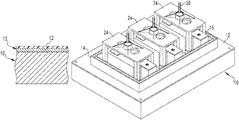
- FIG. 1A is a schematic showing an isometric view of a cooling device, in accordance with the prior art
- FIG. 1B is a schematic showing an isometric view of the cooling device of FIG. 1A with a ceramic coating applied thereto, in accordance with certain embodiments of the disclosed concept;
- FIG. 1C is a schematic showing a cross-section view of the cooling device of FIG. 1B , in accordance with certain embodiments of the disclosed concept;
- FIG. 1D is a schematic showing a cross-section view of the cooling device of FIG. 1A with a ceramic coated plate applied thereto, in accordance with certain embodiments of the disclosed concept;
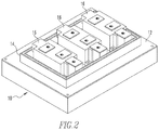
- FIG. 2 is a schematic showing the ceramic coated cooling device of FIG. 1B in combination with a plurality of diodes, in accordance with certain embodiments of the disclosed concept;
- FIG. 3 is a schematic showing the ceramic coated cooling device and diode combination shown in FIG. 2 , with the addition of clamp and swivel devices, in accordance with certain embodiments of the disclosed concept;
- FIG. 3A is a schematic showing a detailed view of one of the clamp and swivel devices of FIG. 3 , in accordance with certain embodiments of the disclosed concept;
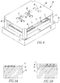
- FIG. 4 is a schematic showing the ceramic coated cooling device and diode combination shown in FIG. 3 with the addition of a framework, in accordance with certain embodiments of the disclosed concept;
- FIG. 5A is a schematic showing the cooling device of FIG. 1C with an intermediate layer directly applied thereto and the ceramic coating directly applied to the intermediate layer, in accordance with certain embodiments of the disclosed concept;
- FIG. 5B is a schematic showing the cooling device of FIG. 1D with an intermediate layer directly applied to the plate and the ceramic coating directly applied to the intermediate layer, in accordance with certain embodiments of the disclosed concept;
- FIG. 6 is a schematic showing a metal mounting device for a cooling device and diode combination, in accordance with certain embodiments of the disclosed concept.
- FIG. 7 is a schematic showing a non-metal mounting device for a cooling device and diode combination, in accordance with certain embodiments of the disclosed concept.
- number shall mean one or an integer greater than one (i.e., a plurality).
- FIG. 1A is a schematic showing a cold plate 10 having a top surface 11 , which is employed as a cooling device associated with power electronic devices in accordance with the prior art.
- Various cooling devices are known in the art, such as, but not limited to liquid cold plates.
- the liquid associated with a cold plate is referred to as a primary cooling source, which can include, but is not limited to, water, refrigerant or phase change medium.
- the disclosed concept can be equally applied to a wide variety of cooling devices.
- FIG. 1B is a schematic showing the cold plate 10 as shown in FIG. 1A .
- FIG. 1B includes a ceramic layer 12 formed on the top surface 11 (shown in FIG. 1A ) of the cold plate 10 .
- the ceramic layer 12 can be formed by depositing or applying a ceramic coating composition directly to the top surface 11 of the cold plate 10 . As shown in FIG. 1B , the ceramic layer 12 extends over the entire top surface 11 of the cold plate 10 . However, it is understood that the ceramic layer 12 may be deposited or applied such that it covers only a portion of the top surface 11 of the cold plate 10 .
- FIG. 1C is a schematic showing a cross-section of the cold plate 10 and the ceramic layer 12 shown in FIG. 1B . As shown in FIG. 1C , the ceramic layer 12 is deposited or applied directly onto the top surface 11 (shown in FIG. 1A ) of the cold plate 10 .
- the ceramic layer 12 can be formed by depositing or applying a ceramic coating composition to a substrate, such as, a metal sheet or metal plate, and connecting the ceramic coated substrate to the cold plate 10 .
- FIG. 1D is a schematic showing a cross-section of the cold plate 10 and the ceramic layer 12 shown in FIG. 1B .
- FIG. 1D includes a substrate 13 , which can be constructed of metal.
- the ceramic layer 12 is directly deposited or applied to a top surface of the substrate 13 , and a bottom surface of the substrate 13 is connected or coupled to the top surface 11 of the cold plate 10 .
- Various mechanisms for connecting or coupling one substrate to another are known in the art.
- the substrate 13 is connected to the cold plate 10 by welding.
- the substrate 13 covers the entire top surface of the cold plate 10 .
- the substrate 13 may cover only a portion of the top surface of the cold plate 10 .
- there may be a recess formed in the top surface of the cold plate 10 , such that the substrate 13 is placed within the recess and therefore, the substrate 13 is flush with the top surface of the cold plate 10 .
- Deposition or application of the ceramic coating composition, e.g., to the cold plate 10 or the substrate 13 , to form a ceramic layer 12 can be accomplished using various conventional apparatus and techniques known in the art, such as, spraying, brushing, wiping and the like.
- the disclosed concept includes the use of pure ceramic compositions, ceramic-based compositions and ceramic-containing compositions.
- Suitable ceramics for use can be selected from a wide variety of ceramics known in the art, such as, but not limited to, boron nitride, alumina, aluminum nitride, silica and mixtures thereof.
- the ceramic composition is Thermolon®, which is commercially available from Porcelain Industries.
- FIG. 2 is a schematic showing the cold plate 10 and the ceramic layer 12 , as shown in FIG. 1B .
- FIG. 2 includes a creep barrier 14 and a plurality of diodes 16 positioned on the top surface 11 (shown in FIG. 1A ) to interface with the cold plate 10 and to contact the ceramic layer 12 .
- the diodes 16 are located within the area that is formed and encompassed by the creep barrier 14 .
- There are three diodes shown in FIG. 2 however, it is contemplated that there can be more or less than three diodes in certain other embodiments of the disclosed concept. For example, there can be a single diode or a plurality of diodes.
- the diodes 16 are representative of a power electronic device for use in accordance with certain embodiments of the disclosed concept; however, it is contemplated that a variety of other power electronic devices are known in the art and can be employed in the disclosed concept. For example, one or more insulated-gate bipolar transistors may be used.
- the ceramic layer 12 extends over the entire top surface 11 of the cold plate 10
- the ceramic layer 12 may be deposited or applied to the cold plate 10 such that it covers only the portion of the top surface 11 that is encompassed by the creep barrier 14 (and the portion of the surface of the cold plate 10 that extends beyond the creep barrier 14 is not covered by the ceramic layer 12 ).
- the creep barrier 14 may be absent.
- FIG. 2 shows a plurality of diodes 16 , it is contemplated that there are a wide variety of power electronic devices known in the art, which are associated with cooling devices, and the disclosed concept can be equally applied to the wide variety of power electronic devices.
- FIG. 3 is a schematic showing the cold plate 10 , ceramic layer 12 , creep barrier 14 and plurality of diodes 16 shown in FIG. 2 .
- FIG. 3 shows a plurality of threaded swivels 20 and a corresponding plurality of clamps 24 .
- Each one of the combined plurality of threaded swivels 20 and clamps 24 is positioned to house a corresponding one of the plurality of diodes 16 .
- FIG. 3A is a schematic showing a detailed view of one of the plurality of clamps 24 .
- each one of the clamps 24 includes an upper surface 25 and a plurality of legs 23 , each of which extends downwardly from a corresponding corner of the upper surface 25 .
- One end of each of the plurality of legs 23 is attached or coupled to the upper surface 25 and the other end of each of the plurality of legs 23 is in contact with the surface of the baseplate of the diode.
- FIG. 4 is a schematic showing the cold plate 10 , ceramic layer 12 , creep barrier 14 , plurality of diodes 16 , plurality of legs 23 and plurality of threaded swivels 20 shown in FIG. 3 .
- FIG. 4 includes a framework 22 .
- the framework 22 has a top canopy 26 and a plurality of extensions 28 , each extending downwardly from the top canopy 26 .
- One end of each of the extensions 28 is attached or coupled to a corner of the canopy 26 .
- the canopy 26 and the plurality of extensions 28 are a single integrated or molded piece.
- An opposite end of each of the plurality of extensions 28 is structured to correspond and connect or fasten to a corner portion of the top surface 11 of the cold plate 10 .
- each of the plurality of extensions 28 can include an aperture 29 , which aligns with an aperture formed in the top surface 11 (shown in FIG. 1A ) of the cold plate 10 .
- a fastening mechanism (not shown), such as, a bolt, can be inserted within each of the apertures to secure the framework 22 to the cold plate 10 .
- the canopy 26 also includes a plurality of swivel apertures (not shown) formed therein and a plurality of nuts 32 , which are structured to receive each of the plurality of threaded swivels 20 . As shown in FIG.
- each of the plurality of threaded swivels 20 is inserted into each of the corresponding plurality of nuts 32 to secure an interface between the plurality of diodes 16 and the cold plate 10 .
- a tip of each of the plurality of the threaded swivels 20 contacts and presses downward on the each of the corresponding plurality of clamps 24 , which causes pressure to be applied to the plurality of diodes 16 in contact with the cooling plate 10 .
- Each of the plurality of threaded swivels 20 is rotated in one direction to apply pressure to each of the corresponding plurality of clamps 24 and is rotated in an opposite direction to release the pressure.
- the ceramic coating composition is deposited or applied directly onto the top surface 11 of the cold plate 10 to form the ceramic layer 12 (shown FIG. 1C ).
- the ceramic coating composition is deposited or applied directly onto a substrate 13 , which is connected to the top surface 11 of the cold plate 10 (shown in FIG. 1D ).
- the surface to be coated e.g., the top surface 11 or the substrate 13
- the surface to be coated can be pre-treated prior to depositing or applying the ceramic coating composition.
- there may be deposited or applied an intermediate layer such that the ceramic coating composition is deposited or applied to the intermediate layer instead of being directly to the top surface 11 of the cold plate 10 or the substrate 13 .
- the intermediate layer may serve various functions, such as, but not limited to, providing enhanced adhesive properties to adhere the ceramic coating composition to the top surface 11 of the cold plate 10 or the substrate 13 .
- Various materials are known in the art for providing adhesive properties to enhance adherence between two surfaces, which can be used in the disclosed concept.
- FIG. 5A shows a cross-section view of the cold plate 10 and ceramic layer 12 shown in FIG. 1C .
- FIG. 5A includes an intermediate layer 34 deposited or applied to the top surface 11 (shown in FIG. 1A ) of the cold plate 10 and the ceramic layer 12 is then formed on top of the intermediate layer 34 , such as, by depositing or applying the ceramic coating composition onto an outer surface of the intermediate layer 34 .
- FIG. 5B shows a cross-section view of the cold plate 10 , ceramic layer 12 and substrate 13 shown in FIG. 1D .
- FIG. 5B includes the intermediate layer 34 deposited or applied to the substrate 13 and the ceramic layer 12 is then formed on top of the intermediate layer 34 , such as, by depositing or applying the ceramic coating composition onto an outer surface of the intermediate layer 34 .
- a fastening mechanism such as, one or more bolts or the like can be employed to mount a cooling device, e.g., a cold plate, with a power electronic device, e.g., a diode.
- a cooling device e.g., a cold plate
- a power electronic device e.g., a diode.
- the use of the one or more bolts as the fastening mechanism requires that one or more corresponding mounting holes or apertures are formed within the cold plate and the diode.
- the one or more bolts contact the diode baseplate and as a result, bypass a ceramic coating that may be applied to the surface of the cold plate and provide a path to ground.
- the surface of the mounting apertures e.g., an internal radial surface, can be coated with a ceramic composition to form a ceramic coating on the surface of the mounting apertures.
- the one or more bolts are composed or constructed of metal.
- the one or more metal bolts can be coated with the ceramic composition.
- the one or bolts may be composed of a non-metal material, such as, but not limited to, plastic or fiberglass.
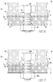
- FIG. 6 shows a power electronic device and associated cooling device combination 50 in accordance with certain embodiments of the disclosed concept.
- the combination 50 includes a diode 52 , a cold device 54 , a mounting aperture 56 , a metal bolt 58 and a metal nut 60 .
- the diode 52 consists of a case 62 and a metal baseplate 64 .
- the metal baseplate 64 can be composed of a wide variety of metals and metal alloys. In certain embodiments, the metal baseplate 64 is composed of alumina silica carbide.
- the mounting aperture 56 extends through the metal baseplate 64 and the cold device 54 .
- the metal bolt 58 has a horizontal portion, a vertical portion and a tip. The horizontal portion of the metal bolt 58 is in contact with the metal baseplate 64 .
- the vertical portion of the metal bolt 58 extends through the mounting aperture 56 .
- the tip of the metal bolt 58 has fitted thereon the metal nut 60 to secure the metal bolt 58 within the mounting aperture 56 and, the interface between the diode 52 and the cold device 54 .
- a ceramic coating composition is deposited or applied to a top surface of the cold device 54 such that the ceramic coating layer 66 is formed at the interface.
- the ceramic coating layer 66 is formed on each of two side surfaces of the cold device 54 , which form the mounting aperture 56 and its radial surface.
- the radial surface of the aperture 56 has applied thereto the ceramic coating layer 66 .
- the ceramic coating layer 66 is applied to a bottom surface of the cold device 54 , such that the metal nut 60 contacts the ceramic coating layer 66 .
- FIG. 7 shows the combination 50 shown in FIG. 6 including the diode 52 , cold device 54 , mounting aperture 56 , case 62 , metal baseplate 64 and ceramic coating layer 66 .
- a non-metal bolt 58 A and a non-metal nut 60 A are used.
- the ceramic coating layer 66 is only applied to the interface of the metal baseplate 64 of the diode 52 and the cold device 54 , and to the interface of the cold device 54 and the mounting aperture 56 .
Landscapes
- Engineering & Computer Science (AREA)
- Microelectronics & Electronic Packaging (AREA)
- Physics & Mathematics (AREA)
- Thermal Sciences (AREA)
- Chemical & Material Sciences (AREA)
- Ceramic Engineering (AREA)
- Cooling Or The Like Of Semiconductors Or Solid State Devices (AREA)
Abstract
Description
Claims (10)
Priority Applications (1)
| Application Number | Priority Date | Filing Date | Title |
|---|---|---|---|
| US14/730,333 US10629513B2 (en) | 2015-06-04 | 2015-06-04 | Ceramic plated materials for electrical isolation and thermal transfer |
Applications Claiming Priority (1)
| Application Number | Priority Date | Filing Date | Title |
|---|---|---|---|
| US14/730,333 US10629513B2 (en) | 2015-06-04 | 2015-06-04 | Ceramic plated materials for electrical isolation and thermal transfer |
Publications (2)
| Publication Number | Publication Date |
|---|---|
| US20160360647A1 US20160360647A1 (en) | 2016-12-08 |
| US10629513B2 true US10629513B2 (en) | 2020-04-21 |
Family
ID=57452834
Family Applications (1)
| Application Number | Title | Priority Date | Filing Date |
|---|---|---|---|
| US14/730,333 Expired - Fee Related US10629513B2 (en) | 2015-06-04 | 2015-06-04 | Ceramic plated materials for electrical isolation and thermal transfer |
Country Status (1)
| Country | Link |
|---|---|
| US (1) | US10629513B2 (en) |
Cited By (1)
| Publication number | Priority date | Publication date | Assignee | Title |
|---|---|---|---|---|
| US10794573B2 (en) * | 2017-07-31 | 2020-10-06 | Signify Holding B.V. | Surge protected luminaire that suppresses parasitic capacitance |
Families Citing this family (2)
| Publication number | Priority date | Publication date | Assignee | Title |
|---|---|---|---|---|
| US11980009B2 (en) | 2019-10-15 | 2024-05-07 | Ciena Corporation | Liquid cooling high-density pluggable modules for a network element |
| US12543295B2 (en) | 2019-10-15 | 2026-02-03 | Ciena Corporation | Hybrid air/liquid-cooled network element, coolant distribution manifold box for use in a hybrid air/liquid-cooled network element, and method for converting an air-cooled network element to a hybrid air/liquid-cooled network element |
Citations (54)
| Publication number | Priority date | Publication date | Assignee | Title |
|---|---|---|---|---|
| US4358541A (en) * | 1981-11-23 | 1982-11-09 | Corning Glass Works | Glass-ceramic coatings for use on metal substrates |
| US4450471A (en) * | 1980-06-21 | 1984-05-22 | Lucas Industries Limited | Semi-conductor power device assembly and method of manufacture thereof |
| US4703339A (en) * | 1985-07-08 | 1987-10-27 | Nec Corporation | Package having a heat sink suitable for a ceramic substrate |
| US4794048A (en) * | 1987-05-04 | 1988-12-27 | Allied-Signal Inc. | Ceramic coated metal substrates for electronic applications |
| US4997698A (en) * | 1987-05-04 | 1991-03-05 | Allied-Signal, Inc. | Ceramic coated metal substrates for electronic applications |
| US5473510A (en) * | 1994-03-25 | 1995-12-05 | Convex Computer Corporation | Land grid array package/circuit board assemblies and methods for constructing the same |
| US5715141A (en) * | 1994-11-07 | 1998-02-03 | Atlas Copco Controls Ab | Control circuit arrangement having a clamping structure which connects a heat conductive substrate to a circuit board and provides electrically conducting leads therebetween |
| US5763946A (en) * | 1995-07-26 | 1998-06-09 | Kabushiki Kaisha Toshiba | Semiconductor device with bent electrode terminal |
| US5814535A (en) * | 1994-04-22 | 1998-09-29 | Nec Corporation | Supporting member for cooling means, electronic package and method of making the same |
| US5841340A (en) * | 1996-05-07 | 1998-11-24 | Rf Power Components, Inc. | Solderless RF power film resistors and terminations |
| US6215185B1 (en) * | 1998-12-11 | 2001-04-10 | Mitsubishi Denki Kabushiki Kaisha | Power semiconductor module |
| US6232151B1 (en) * | 1999-11-01 | 2001-05-15 | General Electric Company | Power electronic module packaging |
| US6233817B1 (en) * | 1999-01-17 | 2001-05-22 | Delphi Technologies, Inc. | Method of forming thick-film hybrid circuit on a metal circuit board |
| US6268239B1 (en) * | 1999-04-20 | 2001-07-31 | Nec Corporation | Semiconductor chip cooling structure and manufacturing method thereof |
| US6285076B1 (en) * | 1997-08-28 | 2001-09-04 | Kabushiki Kaisha Toshiba | Press-connection semiconductor device and press-connection semiconductor assembly |
| US20020034087A1 (en) * | 2000-09-19 | 2002-03-21 | Osamu Suzuki | Electric power conversion/inversion apparatus |
| US20020119079A1 (en) * | 1999-12-10 | 2002-08-29 | Norbert Breuer | Chemical microreactor and microreactor made by process |
| US6455930B1 (en) * | 1999-12-13 | 2002-09-24 | Lamina Ceramics, Inc. | Integrated heat sinking packages using low temperature co-fired ceramic metal circuit board technology |
| US6483185B1 (en) * | 1998-09-22 | 2002-11-19 | Mitsubishi Materials Corporation | Power module substrate, method of producing the same, and semiconductor device including the substrate |
| US20030025196A1 (en) * | 2001-08-01 | 2003-02-06 | Hitachi, Ltd. | Heat transfer structure and a semi-conductor device |
| US6617520B1 (en) * | 2000-08-30 | 2003-09-09 | Heatron, Inc. | Circuit board |
| US20040140116A1 (en) * | 2001-06-25 | 2004-07-22 | Reinhold Bayerer | High voltage module and method for producing same |
| US20040222433A1 (en) * | 2003-05-05 | 2004-11-11 | Lamina Ceramics | Light emitting diodes packaged for high temperature operation |
| US6903941B2 (en) * | 2002-10-24 | 2005-06-07 | Hewlett-Packard Development Company, L.P. | Printed circuit board assembly employing a press fit electrical connector |
| US20050135065A1 (en) * | 2003-12-19 | 2005-06-23 | Hitachi Industrial Equipment Systems Co., Ltd. | Electric circuit module |
| US20060124953A1 (en) * | 2004-12-14 | 2006-06-15 | Negley Gerald H | Semiconductor light emitting device mounting substrates and packages including cavities and cover plates, and methods of packaging same |
| US20070230184A1 (en) * | 2006-03-31 | 2007-10-04 | Shuy Geoffrey W | Heat exchange enhancement |
| US20080151504A1 (en) * | 2006-04-11 | 2008-06-26 | International Business Machines Corporation | System and method for cooling a module |
| US7412898B1 (en) * | 2006-07-28 | 2008-08-19 | Disney Enterprises, Inc. | Load sensing system including RFID tagged fasteners |
| US20080196869A1 (en) * | 2006-04-20 | 2008-08-21 | The Boeing Company | High conductivity ceramic foam cold plate |
| US7475607B2 (en) * | 2004-01-08 | 2009-01-13 | Honeywell International Inc. | Sensing apparatus with an integrated gasket on a beam component |
| US7477519B2 (en) * | 2003-04-16 | 2009-01-13 | Fujitsu Limited | Electronic component package including heat spreading member |
| US20090050957A1 (en) * | 2007-08-24 | 2009-02-26 | Kabushiki Kaisha Toshiba | Semiconductor device and method of manufacturing the same |
| US20090079061A1 (en) * | 2003-03-05 | 2009-03-26 | Debendra Mallik | Thermally enhanced electronic flip-chip packaging with external-connector-side die and method |
| US7746653B2 (en) * | 2008-01-02 | 2010-06-29 | Harman International Industries Incorporated | Clamp for electrical devices |
| US7782621B2 (en) * | 2007-11-06 | 2010-08-24 | International Business Machines Corporation | Circuit module and manufacturing method thereof |
| US20100284155A1 (en) * | 2009-05-11 | 2010-11-11 | Infineon Technologies Ag | Power Semiconductor Module Including Substrates Spaced from Each Other |
| US20100321897A1 (en) * | 2009-06-17 | 2010-12-23 | Laird Technologies, Inc. | Compliant multilayered thermally-conductive interface assemblies |
| US20110044002A1 (en) * | 2008-01-22 | 2011-02-24 | Valtion Teknillinen Tutkimuskeskus | Method for arranging cooling for a component and a cooling element |
| US7906793B2 (en) * | 2004-10-25 | 2011-03-15 | Cree, Inc. | Solid metal block semiconductor light emitting device mounting substrates |
| US20120212175A1 (en) * | 2011-02-17 | 2012-08-23 | Lear Corporation | Sealed battery charger housing |
| US20130063946A1 (en) * | 2010-05-21 | 2013-03-14 | Osram Ag | Lighting apparatus |
| US20130069215A1 (en) * | 2011-09-21 | 2013-03-21 | Kabushiki Kaisha Toshiba | Semiconductor device |
| US20130215613A1 (en) * | 2012-02-17 | 2013-08-22 | Tsmc Solid State Lighting Ltd. | Led packaging structure having improved thermal dissipation and mechanical strength |
| US8519265B2 (en) * | 2009-09-18 | 2013-08-27 | Kabushiki Kaisha Toshiba | Power module |
| US20130241046A1 (en) * | 2010-11-22 | 2013-09-19 | Toshiba Materials Co., Ltd. | Ceramic heat sink material for pressure contact structure, semiconductor module using the same, and method for manufacturing semiconductor module |
| US8547705B2 (en) * | 2009-08-20 | 2013-10-01 | Nec Corporation | Semiconductor device having power supply-side and ground-side metal reinforcing members insulated from each other |
| US20130308274A1 (en) * | 2012-05-21 | 2013-11-21 | Triquint Semiconductor, Inc. | Thermal spreader having graduated thermal expansion parameters |
| US20140167235A1 (en) * | 2012-12-19 | 2014-06-19 | Fuji Electric Co., Ltd. | Semiconductor module |
| US8772817B2 (en) * | 2010-12-22 | 2014-07-08 | Cree, Inc. | Electronic device submounts including substrates with thermally conductive vias |
| US20140347819A1 (en) * | 2011-12-21 | 2014-11-27 | Robert Bosch Gmbh | Electronics Module for a Vehicle |
| US20150260390A1 (en) * | 2014-03-14 | 2015-09-17 | Eric Colin Bretschneider | Composite Heat Sink For Electrical Components |
| US20160057881A1 (en) * | 2014-08-22 | 2016-02-25 | Kabushiki Kaisha Toshiba | Semiconductor device |
| US20160218048A1 (en) * | 2015-01-26 | 2016-07-28 | Nuvotronics Inc. | Microfluidic channels for thermal management of microelectronics |
Family Cites Families (1)
| Publication number | Priority date | Publication date | Assignee | Title |
|---|---|---|---|---|
| US5013948A (en) * | 1987-05-04 | 1991-05-07 | Allied-Signal Inc. | High power rotating rectifier assembly |
-
2015
- 2015-06-04 US US14/730,333 patent/US10629513B2/en not_active Expired - Fee Related
Patent Citations (57)
| Publication number | Priority date | Publication date | Assignee | Title |
|---|---|---|---|---|
| US4450471A (en) * | 1980-06-21 | 1984-05-22 | Lucas Industries Limited | Semi-conductor power device assembly and method of manufacture thereof |
| US4358541A (en) * | 1981-11-23 | 1982-11-09 | Corning Glass Works | Glass-ceramic coatings for use on metal substrates |
| US4703339A (en) * | 1985-07-08 | 1987-10-27 | Nec Corporation | Package having a heat sink suitable for a ceramic substrate |
| US4794048A (en) * | 1987-05-04 | 1988-12-27 | Allied-Signal Inc. | Ceramic coated metal substrates for electronic applications |
| US4997698A (en) * | 1987-05-04 | 1991-03-05 | Allied-Signal, Inc. | Ceramic coated metal substrates for electronic applications |
| US5473510A (en) * | 1994-03-25 | 1995-12-05 | Convex Computer Corporation | Land grid array package/circuit board assemblies and methods for constructing the same |
| US5814535A (en) * | 1994-04-22 | 1998-09-29 | Nec Corporation | Supporting member for cooling means, electronic package and method of making the same |
| US5715141A (en) * | 1994-11-07 | 1998-02-03 | Atlas Copco Controls Ab | Control circuit arrangement having a clamping structure which connects a heat conductive substrate to a circuit board and provides electrically conducting leads therebetween |
| US5763946A (en) * | 1995-07-26 | 1998-06-09 | Kabushiki Kaisha Toshiba | Semiconductor device with bent electrode terminal |
| US5841340A (en) * | 1996-05-07 | 1998-11-24 | Rf Power Components, Inc. | Solderless RF power film resistors and terminations |
| US6285076B1 (en) * | 1997-08-28 | 2001-09-04 | Kabushiki Kaisha Toshiba | Press-connection semiconductor device and press-connection semiconductor assembly |
| US6483185B1 (en) * | 1998-09-22 | 2002-11-19 | Mitsubishi Materials Corporation | Power module substrate, method of producing the same, and semiconductor device including the substrate |
| US6215185B1 (en) * | 1998-12-11 | 2001-04-10 | Mitsubishi Denki Kabushiki Kaisha | Power semiconductor module |
| US6233817B1 (en) * | 1999-01-17 | 2001-05-22 | Delphi Technologies, Inc. | Method of forming thick-film hybrid circuit on a metal circuit board |
| US6268239B1 (en) * | 1999-04-20 | 2001-07-31 | Nec Corporation | Semiconductor chip cooling structure and manufacturing method thereof |
| US6232151B1 (en) * | 1999-11-01 | 2001-05-15 | General Electric Company | Power electronic module packaging |
| US20020119079A1 (en) * | 1999-12-10 | 2002-08-29 | Norbert Breuer | Chemical microreactor and microreactor made by process |
| US6455930B1 (en) * | 1999-12-13 | 2002-09-24 | Lamina Ceramics, Inc. | Integrated heat sinking packages using low temperature co-fired ceramic metal circuit board technology |
| US6617520B1 (en) * | 2000-08-30 | 2003-09-09 | Heatron, Inc. | Circuit board |
| US20020034087A1 (en) * | 2000-09-19 | 2002-03-21 | Osamu Suzuki | Electric power conversion/inversion apparatus |
| US20040140116A1 (en) * | 2001-06-25 | 2004-07-22 | Reinhold Bayerer | High voltage module and method for producing same |
| US20030025196A1 (en) * | 2001-08-01 | 2003-02-06 | Hitachi, Ltd. | Heat transfer structure and a semi-conductor device |
| US6903941B2 (en) * | 2002-10-24 | 2005-06-07 | Hewlett-Packard Development Company, L.P. | Printed circuit board assembly employing a press fit electrical connector |
| US20090079061A1 (en) * | 2003-03-05 | 2009-03-26 | Debendra Mallik | Thermally enhanced electronic flip-chip packaging with external-connector-side die and method |
| US7477519B2 (en) * | 2003-04-16 | 2009-01-13 | Fujitsu Limited | Electronic component package including heat spreading member |
| US20040222433A1 (en) * | 2003-05-05 | 2004-11-11 | Lamina Ceramics | Light emitting diodes packaged for high temperature operation |
| US20050135065A1 (en) * | 2003-12-19 | 2005-06-23 | Hitachi Industrial Equipment Systems Co., Ltd. | Electric circuit module |
| US7475607B2 (en) * | 2004-01-08 | 2009-01-13 | Honeywell International Inc. | Sensing apparatus with an integrated gasket on a beam component |
| US7906793B2 (en) * | 2004-10-25 | 2011-03-15 | Cree, Inc. | Solid metal block semiconductor light emitting device mounting substrates |
| US20060124953A1 (en) * | 2004-12-14 | 2006-06-15 | Negley Gerald H | Semiconductor light emitting device mounting substrates and packages including cavities and cover plates, and methods of packaging same |
| US20070230184A1 (en) * | 2006-03-31 | 2007-10-04 | Shuy Geoffrey W | Heat exchange enhancement |
| US20080151504A1 (en) * | 2006-04-11 | 2008-06-26 | International Business Machines Corporation | System and method for cooling a module |
| US7558066B2 (en) * | 2006-04-11 | 2009-07-07 | International Business Machines Corporation | System and method for cooling a module |
| US20080196869A1 (en) * | 2006-04-20 | 2008-08-21 | The Boeing Company | High conductivity ceramic foam cold plate |
| US7412898B1 (en) * | 2006-07-28 | 2008-08-19 | Disney Enterprises, Inc. | Load sensing system including RFID tagged fasteners |
| US7768109B2 (en) * | 2007-08-24 | 2010-08-03 | Kabushiki Kaisha Toshiba | Semiconductor device and method of manufacturing the same |
| US20090050957A1 (en) * | 2007-08-24 | 2009-02-26 | Kabushiki Kaisha Toshiba | Semiconductor device and method of manufacturing the same |
| US7782621B2 (en) * | 2007-11-06 | 2010-08-24 | International Business Machines Corporation | Circuit module and manufacturing method thereof |
| US7746653B2 (en) * | 2008-01-02 | 2010-06-29 | Harman International Industries Incorporated | Clamp for electrical devices |
| US20110044002A1 (en) * | 2008-01-22 | 2011-02-24 | Valtion Teknillinen Tutkimuskeskus | Method for arranging cooling for a component and a cooling element |
| US8514579B2 (en) * | 2009-05-11 | 2013-08-20 | Infineon Technologies Ag | Power semiconductor module including substrates spaced from each other |
| US20100284155A1 (en) * | 2009-05-11 | 2010-11-11 | Infineon Technologies Ag | Power Semiconductor Module Including Substrates Spaced from Each Other |
| US20100321897A1 (en) * | 2009-06-17 | 2010-12-23 | Laird Technologies, Inc. | Compliant multilayered thermally-conductive interface assemblies |
| US8547705B2 (en) * | 2009-08-20 | 2013-10-01 | Nec Corporation | Semiconductor device having power supply-side and ground-side metal reinforcing members insulated from each other |
| US8519265B2 (en) * | 2009-09-18 | 2013-08-27 | Kabushiki Kaisha Toshiba | Power module |
| US20130063946A1 (en) * | 2010-05-21 | 2013-03-14 | Osram Ag | Lighting apparatus |
| US20130241046A1 (en) * | 2010-11-22 | 2013-09-19 | Toshiba Materials Co., Ltd. | Ceramic heat sink material for pressure contact structure, semiconductor module using the same, and method for manufacturing semiconductor module |
| US8772817B2 (en) * | 2010-12-22 | 2014-07-08 | Cree, Inc. | Electronic device submounts including substrates with thermally conductive vias |
| US20120212175A1 (en) * | 2011-02-17 | 2012-08-23 | Lear Corporation | Sealed battery charger housing |
| US20130069215A1 (en) * | 2011-09-21 | 2013-03-21 | Kabushiki Kaisha Toshiba | Semiconductor device |
| US20140347819A1 (en) * | 2011-12-21 | 2014-11-27 | Robert Bosch Gmbh | Electronics Module for a Vehicle |
| US20130215613A1 (en) * | 2012-02-17 | 2013-08-22 | Tsmc Solid State Lighting Ltd. | Led packaging structure having improved thermal dissipation and mechanical strength |
| US20130308274A1 (en) * | 2012-05-21 | 2013-11-21 | Triquint Semiconductor, Inc. | Thermal spreader having graduated thermal expansion parameters |
| US20140167235A1 (en) * | 2012-12-19 | 2014-06-19 | Fuji Electric Co., Ltd. | Semiconductor module |
| US20150260390A1 (en) * | 2014-03-14 | 2015-09-17 | Eric Colin Bretschneider | Composite Heat Sink For Electrical Components |
| US20160057881A1 (en) * | 2014-08-22 | 2016-02-25 | Kabushiki Kaisha Toshiba | Semiconductor device |
| US20160218048A1 (en) * | 2015-01-26 | 2016-07-28 | Nuvotronics Inc. | Microfluidic channels for thermal management of microelectronics |
Cited By (1)
| Publication number | Priority date | Publication date | Assignee | Title |
|---|---|---|---|---|
| US10794573B2 (en) * | 2017-07-31 | 2020-10-06 | Signify Holding B.V. | Surge protected luminaire that suppresses parasitic capacitance |
Also Published As
| Publication number | Publication date |
|---|---|
| US20160360647A1 (en) | 2016-12-08 |
Similar Documents
| Publication | Publication Date | Title |
|---|---|---|
| EP2784810B1 (en) | Chip packaging structure and chip packaging method | |
| US10064287B2 (en) | System and method of providing a semiconductor carrier and redistribution structure | |
| US20150334871A1 (en) | Thermal interface materials with thin film sealants | |
| US20150035138A1 (en) | Semiconductor device | |
| US10629513B2 (en) | Ceramic plated materials for electrical isolation and thermal transfer | |
| GB2422249A (en) | Power substrate | |
| US10522442B2 (en) | Dissipating heat from an electronic device in a protective housing | |
| JP6160698B2 (en) | Semiconductor device | |
| US12133366B2 (en) | Power electronics module with improved cooling | |
| US20150040388A1 (en) | Application of Dielectric Layer and Circuit Traces on Heat Sink | |
| JP2019021864A (en) | Power module | |
| CN110379783B (en) | Method and structure for improving insulation and heat dissipation performance of semiconductor device relative to heat sink | |
| US10784183B2 (en) | Semiconductor module with package extension frames | |
| US10403566B2 (en) | Power module | |
| US20170055369A1 (en) | Ceramic coated flow channels for electrical isolation and thermal transfer | |
| JP5087048B2 (en) | Circuit board with integrated heat dissipation components | |
| US20200181407A1 (en) | Electronics packaging using organic electrically insulating layers | |
| CN105206589A (en) | A method of heat transfer in power electronics applications | |
| US11081421B2 (en) | IGBT module with heat dissipation structure having ceramic layers corresponding in position and in area to chips | |
| US12127329B2 (en) | Flexible circuit board with thermally conductive connection to a heat sink | |
| CN208093538U (en) | Power semiconductor component module with pressure plate forming basin | |
| US20200185303A1 (en) | Igbt module with improved heat dissipation structure | |
| JP2015228400A (en) | Heat dissipation structure of substrate element | |
| CN112786545A (en) | Semiconductor device package and method of manufacturing the same | |
| CN207441689U (en) | Intelligent power module and air conditioner |
Legal Events
| Date | Code | Title | Description |
|---|---|---|---|
| AS | Assignment |
Owner name: EATON CORPORATION, OHIO Free format text: ASSIGNMENT OF ASSIGNORS INTEREST;ASSIGNORS:WOOLARD, DAVID GLENN;MURRAY, PAUL THOMAS;SIGNING DATES FROM 20150302 TO 20150526;REEL/FRAME:035784/0751 |
|
| STPP | Information on status: patent application and granting procedure in general |
Free format text: FINAL REJECTION MAILED |
|
| AS | Assignment |
Owner name: EATON INTELLIGENT POWER LIMITED, IRELAND Free format text: ASSIGNMENT OF ASSIGNORS INTEREST;ASSIGNOR:EATON CORPORATION;REEL/FRAME:048855/0626 Effective date: 20171231 |
|
| STPP | Information on status: patent application and granting procedure in general |
Free format text: RESPONSE AFTER FINAL ACTION FORWARDED TO EXAMINER |
|
| STPP | Information on status: patent application and granting procedure in general |
Free format text: NON FINAL ACTION MAILED |
|
| STPP | Information on status: patent application and granting procedure in general |
Free format text: RESPONSE TO NON-FINAL OFFICE ACTION ENTERED AND FORWARDED TO EXAMINER |
|
| STPP | Information on status: patent application and granting procedure in general |
Free format text: NOTICE OF ALLOWANCE MAILED -- APPLICATION RECEIVED IN OFFICE OF PUBLICATIONS |
|
| STCF | Information on status: patent grant |
Free format text: PATENTED CASE |
|
| FEPP | Fee payment procedure |
Free format text: MAINTENANCE FEE REMINDER MAILED (ORIGINAL EVENT CODE: REM.); ENTITY STATUS OF PATENT OWNER: LARGE ENTITY |
|
| LAPS | Lapse for failure to pay maintenance fees |
Free format text: PATENT EXPIRED FOR FAILURE TO PAY MAINTENANCE FEES (ORIGINAL EVENT CODE: EXP.); ENTITY STATUS OF PATENT OWNER: LARGE ENTITY |
|
| STCH | Information on status: patent discontinuation |
Free format text: PATENT EXPIRED DUE TO NONPAYMENT OF MAINTENANCE FEES UNDER 37 CFR 1.362 |
|
| STCH | Information on status: patent discontinuation |
Free format text: PATENT EXPIRED DUE TO NONPAYMENT OF MAINTENANCE FEES UNDER 37 CFR 1.362 |
|
| FP | Lapsed due to failure to pay maintenance fee |
Effective date: 20240421 |