EP1187192A2 - Verfahren zur Herstellung einer elektrisch leitenden Verbindung - Google Patents
Verfahren zur Herstellung einer elektrisch leitenden Verbindung Download PDFInfo
- Publication number
- EP1187192A2 EP1187192A2 EP01120084A EP01120084A EP1187192A2 EP 1187192 A2 EP1187192 A2 EP 1187192A2 EP 01120084 A EP01120084 A EP 01120084A EP 01120084 A EP01120084 A EP 01120084A EP 1187192 A2 EP1187192 A2 EP 1187192A2
- Authority
- EP
- European Patent Office
- Prior art keywords
- conductive material
- layer
- contact hole
- insulating layer
- conductive
- Prior art date
- Legal status (The legal status is an assumption and is not a legal conclusion. Google has not performed a legal analysis and makes no representation as to the accuracy of the status listed.)
- Withdrawn
Links
Images


Classifications
-
- H—ELECTRICITY
- H10—SEMICONDUCTOR DEVICES; ELECTRIC SOLID-STATE DEVICES NOT OTHERWISE PROVIDED FOR
- H10D—INORGANIC ELECTRIC SEMICONDUCTOR DEVICES
- H10D64/00—Electrodes of devices having potential barriers
- H10D64/01—Manufacture or treatment
- H10D64/011—Manufacture or treatment of electrodes ohmically coupled to a semiconductor
-
- H—ELECTRICITY
- H10—SEMICONDUCTOR DEVICES; ELECTRIC SOLID-STATE DEVICES NOT OTHERWISE PROVIDED FOR
- H10W—GENERIC PACKAGES, INTERCONNECTIONS, CONNECTORS OR OTHER CONSTRUCTIONAL DETAILS OF DEVICES COVERED BY CLASS H10
- H10W20/00—Interconnections in chips, wafers or substrates
- H10W20/01—Manufacture or treatment
- H10W20/031—Manufacture or treatment of conductive parts of the interconnections
- H10W20/032—Manufacture or treatment of conductive parts of the interconnections of conductive barrier, adhesion or liner layers
- H10W20/033—Manufacture or treatment of conductive parts of the interconnections of conductive barrier, adhesion or liner layers in openings in dielectrics
- H10W20/036—Manufacture or treatment of conductive parts of the interconnections of conductive barrier, adhesion or liner layers in openings in dielectrics the barrier, adhesion or liner layers being within a main fill metal
-
- H—ELECTRICITY
- H10—SEMICONDUCTOR DEVICES; ELECTRIC SOLID-STATE DEVICES NOT OTHERWISE PROVIDED FOR
- H10B—ELECTRONIC MEMORY DEVICES
- H10B12/00—Dynamic random access memory [DRAM] devices
- H10B12/01—Manufacture or treatment
- H10B12/02—Manufacture or treatment for one transistor one-capacitor [1T-1C] memory cells
- H10B12/03—Making the capacitor or connections thereto
- H10B12/033—Making the capacitor or connections thereto the capacitor extending over the transistor
- H10B12/0335—Making a connection between the transistor and the capacitor, e.g. plug
-
- H—ELECTRICITY
- H10—SEMICONDUCTOR DEVICES; ELECTRIC SOLID-STATE DEVICES NOT OTHERWISE PROVIDED FOR
- H10W—GENERIC PACKAGES, INTERCONNECTIONS, CONNECTORS OR OTHER CONSTRUCTIONAL DETAILS OF DEVICES COVERED BY CLASS H10
- H10W20/00—Interconnections in chips, wafers or substrates
- H10W20/01—Manufacture or treatment
- H10W20/031—Manufacture or treatment of conductive parts of the interconnections
- H10W20/032—Manufacture or treatment of conductive parts of the interconnections of conductive barrier, adhesion or liner layers
- H10W20/046—Manufacture or treatment of conductive parts of the interconnections of conductive barrier, adhesion or liner layers the barrier, adhesion or liner layers being associated with interconnections of capacitors
-
- H—ELECTRICITY
- H10—SEMICONDUCTOR DEVICES; ELECTRIC SOLID-STATE DEVICES NOT OTHERWISE PROVIDED FOR
- H10W—GENERIC PACKAGES, INTERCONNECTIONS, CONNECTORS OR OTHER CONSTRUCTIONAL DETAILS OF DEVICES COVERED BY CLASS H10
- H10W20/00—Interconnections in chips, wafers or substrates
- H10W20/01—Manufacture or treatment
- H10W20/031—Manufacture or treatment of conductive parts of the interconnections
- H10W20/056—Manufacture or treatment of conductive parts of the interconnections by filling conductive material into holes, grooves or trenches
-
- H—ELECTRICITY
- H10—SEMICONDUCTOR DEVICES; ELECTRIC SOLID-STATE DEVICES NOT OTHERWISE PROVIDED FOR
- H10W—GENERIC PACKAGES, INTERCONNECTIONS, CONNECTORS OR OTHER CONSTRUCTIONAL DETAILS OF DEVICES COVERED BY CLASS H10
- H10W20/00—Interconnections in chips, wafers or substrates
- H10W20/01—Manufacture or treatment
- H10W20/071—Manufacture or treatment of dielectric parts thereof
- H10W20/081—Manufacture or treatment of dielectric parts thereof by forming openings in the dielectric parts
- H10W20/082—Manufacture or treatment of dielectric parts thereof by forming openings in the dielectric parts the openings being tapered via holes
-
- H—ELECTRICITY
- H10—SEMICONDUCTOR DEVICES; ELECTRIC SOLID-STATE DEVICES NOT OTHERWISE PROVIDED FOR
- H10D—INORGANIC ELECTRIC SEMICONDUCTOR DEVICES
- H10D1/00—Resistors, capacitors or inductors
- H10D1/60—Capacitors
- H10D1/68—Capacitors having no potential barriers
- H10D1/692—Electrodes
-
- Y—GENERAL TAGGING OF NEW TECHNOLOGICAL DEVELOPMENTS; GENERAL TAGGING OF CROSS-SECTIONAL TECHNOLOGIES SPANNING OVER SEVERAL SECTIONS OF THE IPC; TECHNICAL SUBJECTS COVERED BY FORMER USPC CROSS-REFERENCE ART COLLECTIONS [XRACs] AND DIGESTS
- Y10—TECHNICAL SUBJECTS COVERED BY FORMER USPC
- Y10T—TECHNICAL SUBJECTS COVERED BY FORMER US CLASSIFICATION
- Y10T29/00—Metal working
- Y10T29/49—Method of mechanical manufacture
- Y10T29/49002—Electrical device making
- Y10T29/49117—Conductor or circuit manufacturing
- Y10T29/49124—On flat or curved insulated base, e.g., printed circuit, etc.
- Y10T29/49128—Assembling formed circuit to base
-
- Y—GENERAL TAGGING OF NEW TECHNOLOGICAL DEVELOPMENTS; GENERAL TAGGING OF CROSS-SECTIONAL TECHNOLOGIES SPANNING OVER SEVERAL SECTIONS OF THE IPC; TECHNICAL SUBJECTS COVERED BY FORMER USPC CROSS-REFERENCE ART COLLECTIONS [XRACs] AND DIGESTS
- Y10—TECHNICAL SUBJECTS COVERED BY FORMER USPC
- Y10T—TECHNICAL SUBJECTS COVERED BY FORMER US CLASSIFICATION
- Y10T29/00—Metal working
- Y10T29/49—Method of mechanical manufacture
- Y10T29/49002—Electrical device making
- Y10T29/49117—Conductor or circuit manufacturing
- Y10T29/49124—On flat or curved insulated base, e.g., printed circuit, etc.
- Y10T29/49155—Manufacturing circuit on or in base
-
- Y—GENERAL TAGGING OF NEW TECHNOLOGICAL DEVELOPMENTS; GENERAL TAGGING OF CROSS-SECTIONAL TECHNOLOGIES SPANNING OVER SEVERAL SECTIONS OF THE IPC; TECHNICAL SUBJECTS COVERED BY FORMER USPC CROSS-REFERENCE ART COLLECTIONS [XRACs] AND DIGESTS
- Y10—TECHNICAL SUBJECTS COVERED BY FORMER USPC
- Y10T—TECHNICAL SUBJECTS COVERED BY FORMER US CLASSIFICATION
- Y10T29/00—Metal working
- Y10T29/49—Method of mechanical manufacture
- Y10T29/49002—Electrical device making
- Y10T29/49117—Conductor or circuit manufacturing
- Y10T29/49124—On flat or curved insulated base, e.g., printed circuit, etc.
- Y10T29/49155—Manufacturing circuit on or in base
- Y10T29/49156—Manufacturing circuit on or in base with selective destruction of conductive paths
-
- Y—GENERAL TAGGING OF NEW TECHNOLOGICAL DEVELOPMENTS; GENERAL TAGGING OF CROSS-SECTIONAL TECHNOLOGIES SPANNING OVER SEVERAL SECTIONS OF THE IPC; TECHNICAL SUBJECTS COVERED BY FORMER USPC CROSS-REFERENCE ART COLLECTIONS [XRACs] AND DIGESTS
- Y10—TECHNICAL SUBJECTS COVERED BY FORMER USPC
- Y10T—TECHNICAL SUBJECTS COVERED BY FORMER US CLASSIFICATION
- Y10T29/00—Metal working
- Y10T29/49—Method of mechanical manufacture
- Y10T29/49002—Electrical device making
- Y10T29/49117—Conductor or circuit manufacturing
- Y10T29/49124—On flat or curved insulated base, e.g., printed circuit, etc.
- Y10T29/49155—Manufacturing circuit on or in base
- Y10T29/49165—Manufacturing circuit on or in base by forming conductive walled aperture in base
Definitions
- the invention relates to a method for producing electrically conductive connections through one or more insulating layers, such as for the Connection of storage capacitors with the Selection transistors in highly integrated FRAMs and DRAMs can be used.
- Electrically conductive components are used in highly integrated components Connections or contacts usually between electrically conductive sections, which are in different structural levels, an electrical To allow current flow. According to the material of the it comes to the upper or lower conductive structure level for example to silicon / silicon contacts, Metal / silicon contacts or metal / metal contacts.
- a damascene process is often used to produce such contacts.
- a contact hole is etched with a photolithographic step through one (or more) insulating layer (s) to an underlying connection.
- This is followed by coating with a conductive material, usually doped polysilicon, which completely fills the etched contact hole.
- a CMP step C hemical- M echanical P olishing
- Typical barrier layers are, for example, iridium or Iridium oxide.
- the barrier is usually made the polysilicon by an etching step from an upper part of the contact hole removed.
- barrier material deposited and structured by a CMP step so that the barrier material only in the upper part of the contact hole remains. The barrier material is preferred by deposited a sputtering process.
- the first barrier layer covers the polysilicon Contact and usually prevents the diffusion of Silicon atoms through the barrier.
- the second Barrier layer covers the first barrier layer and usually prevents the diffusion of oxygen through the barrier.
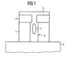
- Fig. 1 there is lower insulating layer 1 on the semiconductor substrate 5 a BPSG silicon oxide, while the top insulating Layer 2 made of a silicon oxide produced in the TEOS process consists.
- the conductive filler layer 3 is made made of polysilicon.
- the cavity 4 arises during coating with the polysilicon in that the opening of the upper Oxide layer because of the smaller diameter before complete filling.
- Overetching trench around the second barrier layer Help of the Damascene method at first Applying a barrier layer in the contact hole area must Mask can be structured on the substrate, the one corresponding opening on the bushing must have. At the The mask can be etched, e.g. because of lack Control options, easily overetched, so that is etched past the side of the first barrier layer, so that a trench forms next to the first barrier layer. This overetching trench can lead to e.g. the still second barrier layer to be applied at the edge in the opening comes into contact with the liner or with the polysilicon, so that it can oxidize the polysilicon or others unwanted chemical reactions that comes about Can cause contact problems.
- Figures 2a and 2b show two conditions under which overetch trenches in one insulating layer 10 can arise: in Fig. 2a is the Mask opening larger than the surface of the first Barrier layer 11 and adhesive layer 12, so that there is an overetch trench 15 around the first barrier layer 11 and the adhesive layer 12 forms around. A subsequent second barrier layer would Fill overetch trench 15 and get in contact with the liner come. 2b, an overetch trench 15 is formed laterally due to misalignment of the mask opening with respect to Surface of the first barrier layer 11 and the Bonding layer 12. A second barrier layer would fill the overetch pit and in this example in Contact with the liner 12 and the polysilicon filling 13 come.
- Dielectric termination for a good one and highly conductive adhesive contact on the polysilicon layer the first barrier layer usually requires one Adhesion layer, preferably a liner, as Interlayer. However, the liner can be in contact with the second barrier layer react chemically, resulting in a dielectric close-off can result. The liner should therefore not even with the lower electrode or the Capacitor dielectric are in contact. In the Care must therefore be taken to manufacture the barrier layers that liner and second barrier layer are not in Come into contact. 3 and 4 show two variants a conductive connection through an insulating layer 10 on a semiconductor substrate 5 according to the prior art, where the unwanted touches between Bonding layer 12 and second barrier layer 17 occur.
- FIG. 3 is a platinum layer 18 on the second barrier layer 17 applied, which in turn on a first barrier layer 11, one Bonding layer 12 and a polysilicon layer 13 rests.
- the critical transition points between the second Barrier layer 17 and adhesive layer 12 are on Edge of the adhesive layer. It is not much different Problem in Fig. 4.
- the present invention is therefore based on the object based on a method of manufacturing an electrical Specify conductive connection that allows the to reduce the described difficulties or entirely avoid and the number of process steps as possible keep it low or even reduce it.
- the process according to the invention has the advantage that you can create a wine glass-like one with just one mask step Contact hole shape can be obtained, which is essentially the Need for a contact hole with smaller Contact hole area in the anisotropically etched area and one larger contact hole area in the isotropically etched area comes close.
- This contact hole shape facilitated by the larger top opening a complete fill with both first as well as with the second conductive material.
- the larger diameter in the upper Sputtering division to separate the second conductive material can be used.
- this contact hole shape enables a conductive one Connection from a very small contact on the bottom the insulating layers, e.g. a diffusion area of a Selection transistor, to a structure on top of the insulating layers that have slightly more lateral space can take such as a lower electrode of a Storage capacitor.
- the larger opening of the contact hole in the upper area further enables that for the etching one on the Contact hole to be structured, e.g. for another conductive material on the second conductive material the second conductive material serves as an etch stop, so that it does not have to the overetched trenches described the problems that come with it.
- this is Ratio of the contact hole area in the isotropically etched area to the contact hole area in the anisotropically etched area between 1.5 and 4, preferably between 2 and 3. Furthermore, it is preferred if the first conductive material is at most to to the anisotropically etched area of the contact hole is etched back. This prevents the second conductive material in the narrower anisotropically etched area the contact hole must be deposited.
- first conductive material and the second conductive material an adhesion promoting layer, in particular titanium, titanium nitride, titanium silicide, tantalum nitride or tantalum silicon nitride. It is particularly preferred if the structuring of the Bonding layer and the second conductive material through a common single or multi-stage CMP step he follows.
- a third conductive Material is applied to the second conductive material.
- the second conductive material as a landing pad for the third conductive material used. That way it is Bonding layer through the second conductive material against direct contact with the third conductive material protected. It is particularly preferred if that third conductive material using a CMP process is structured.
- the contact hole through the second conductive Material has not yet been filled completely, so that the third conductive material in the still free area of the contact hole can be deposited. In this way, another Mask level that would otherwise be used to structure the third conductive material would have been saved become. This configuration also applies no direct contact between the adhesive layer and the third conductive material.
- the Structuring of the second and third senior Material (and possibly the adhesion promoter layer) through a common single or multi-stage CMP step he follows. It can be advantageous here if the CMP process for the third conductive material selective to that second conductive material. That way they can controllable separately from each other by the polishing liquid is removed.
- the present Invention is doped as the first conductive material Polysilicon used. It is further preferred if as second and / or third conductive material Barrier material is used. It is special preferred if a as the second conductive material Barrier material to suppress the diffusion of Silicon atoms, especially iridium, is used. Furthermore, it is preferred if as the third conductive Material is a barrier material to suppress diffusion of oxygen atoms, especially iridium oxide becomes. For example, the conductive connections between the selection transistors and the Storage capacitors in ferroelectric memory cells be generated. Accordingly, the lower one Electrode layer of a ferroelectric capacitor the third conductive material can be applied.
- the etching stop layer before the application of the Electrode layer at the later contact point of the electrode is opened.
- the lower electrode of the storage capacitor can, for example, by a Damascene process be structured.
- the etch stop layer protects the following removal of one during the Damascene procedure used oxide layer before overetch trenches. Is preferred this oxide layer then removed again in order to Sidewalls of the lower electrode as capacitive To have space available for storing cargo.
- the Insulation layer from a lower insulating layer, an upper insulating layer and possibly another insulating layers in between.
- the isotropic etching extends to the bottom insulating layer. Because this way possible contact hole steps in the wide, isrop etched Contact hole area, the formation of voids during the deposition of the first conductive material can be reliably prevented.
- Figure 5 shows a semiconductor substrate 5 with a Selection transistor 54 on the surface, which consists of two Diffusion areas 52 and a gate 53 exists.
- the isolating Layer 50 is a silicon oxide, preferably a BPSG oxide or a Silicon oxide from a TEOS process.
- the Openings Positions of the contact holes to be created define.
- Figure 6 shows the same structure after the isotropic and then the anisotropic etching was carried out are.
- this is similar to wine glass Contact hole recognizable, which is obtained when the mask opening is essentially circular.
- the "goblet" of the wine glass is obtained by the isotropic etching 58, while the “stem” of the wine glass has been achieved by the anisotropic etching 59 is.
- the diameter of the stem is essentially through given the diameter of the mask opening.
- this advantageous contact hole shape with only one Mask step has been reached.
- the ratio of the contact hole area F on the surface in the isotropically etched area to the Contact hole area f in the anisotropically etched area about 2.5.
- FIG. 7 shows the structure after the mask 57 removed, cleaned by means of an HF dip and the contact hole 6 has been filled with conductive materials.
- the filling is in the exemplary embodiment by the following steps Polysilicon is processed in a CVD process on the insulating layer provided with the contact hole 6 50 applied and then by etching or polishing again down to the surface of the insulating layer 50 ablated. By further etching it will be in the contact hole some of the remaining polysilicon from top to one predetermined depth removed so that a Polysilicon layer 60 (first conductive material) produced has been.
- the surface of the polysilicon layer 60 lies preferably in the isotropically etched area.
- a thin one Bonding layer 62 preferably titanium, titanium nitride, Titanium silicide, tantalum nitride or tantalum silicon nitride
- a thick first barrier layer 63 preferably consists of Iridium, which completely fills the contact hole applied conventional method and preferably in one common CMP step up to the surface of the insulating layer 50 removed.
- the first Barrier layer 63 represents the second conductive layer Material.
- Figure 8 shows the next steps.
- a layer of mask 65 from e.g. Silicon oxide is made using conventional methods applied and structured so that the mask openings with the contact holes collapse.
- the mask openings are chosen so small that they completely from the Surface of the first barrier layer 63 are covered. at the first barrier layer 63 can thus be etched can be used as an etch stop, what the destructive effects of the overetch trenches shown in FIG. 2.
- the application and structuring of the second Barrier layer 64 (third conductive material) preferred Iridiumoxid, on the mask layer 65 using the Damascene 's procedure takes place according to the state of the Technology.
- a layer for the lower electrode 70 preferably made of a noble metal or one of its oxides, especially platinum, on the second Barrier layer 64 can be grown.
- the subsequent one Structuring of the lower electrode layer 70 can e.g. by the RIE etching known from the prior art happen (Fig. 9).
- the structuring of the layer for the lower electrode 70 with another Damascene Process step take place, in addition to that for required mask layer also an etch stop layer 71 is applied below the mask layer (Fig. 10).
- the Etching protection layer is advantageous because the mask after the Structuring of the lower electrode 70 removed again to also have the side walls of the lower electrode 70 to be able to cover a dielectric layer. The latter allows maximum capacity with minimal lateral Expansion of the storage capacitor to be manufactured.
- Figure 11 shows the final steps in the Design according to the invention for producing the Storage capacitors on the contact hole: first one thin dielectric layer 73 on the lower electrode 70 and Surroundings, followed by the upper one Electrode layer 75.
- the Dielectric layer 73 made of SBT and the upper one Electrode layer 75 made of platinum.
- FIGs. 12-15 Another embodiment according to the invention will shown in Figs. 12-15. Unlike the previous one execution according to the invention takes place this execution an insulating layer a lower insulating layer 100 and an upper insulating layer 102.
- Farther first, second and third conductive material are velvet Adhesion promoting layer housed in the contact hole, so that at least one mask step is saved.
- FIG. 12 shows the semiconductor substrate 5 with an applied one lower insulating layer 100, upper insulating layer 102 and the mask 57, after an isotropic and then an anisotropic etch on a substantially round one Mask opening from top insulating layer 102 to Diffusion region 52 has been performed.
- This Etching order leads, as in Fig. 6, to a wine glass-like Contact hole 6 with an isotropic etching hole area 58 and one anisotropic etched hole area 59.
- FIG. 12 differs from Fig. 6 only by the presence of two isolating Layers.
- the lower insulating layer is preferably a BPSG oxide
- the upper insulating layer preferably an im Silicon oxide applied using the TEOS process.
- FIG. 13 shows the semiconductor substrate 5 after the Mask 57 has been removed and the semiconductor substrate 5 has been subjected to an HF dip for cleaning.
- This Cleaning step is usually done before applying the Polysilicon layer performed, but causes a selective Etching between the two oxides of the lower insulating Layer 100 and top insulating layer 102.
- contact hole step 104 is broad isotropic etching region 58, it represents for the now subsequent filling with conductive materials is not a problem.
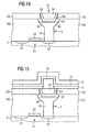
- Fig. 14 shows the contact hole 6 after filling with the three conductive layers and the adhesive layer 62 with the following steps: after the HF dip a Polysilicon layer applied so that the contact hole 6th is filled. Then the polysilicon layer is up to on the surface of the upper insulating layer 102 again removed, e.g. by etching or a CMP step so that the polysilicon only remains in contact hole 6. By The polysilicon in contact hole 6 is then further etched etched to the extent that further conductive layers in the Contact hole can be accommodated. In a preferred one Execution, the further etching will only go so far that the Surface of the polysilicon layer is still isotropic Etched hole area 58 remains. That way is one Polysilicon layer 60, which is the first conductive material of the Claim 1 corresponds to been applied.
- An adhesion promoter layer 62 i.e. a liner, preferably titanium, titanium nitride, titanium silicide, Tantalum nitride or tantalum silicon nitride, then a first Barrier layer 63, the second conductive material of the Corresponds to claim 1 and a second barrier layer 64, which corresponds to the third conductive material of claim 1 applied and by a single, double or three-stage CMP step etched so that all three conductive materials, i.e. polysilicon layer 60, the first barrier layer 63 and the second barrier layer 64 together Adhesion layer 62 housed in the contact hole 6 are. This procedure saves most mask steps and CMP steps for creating a conductive connection through insulating layers with three conductive materials on.
- Preferred materials of the first barrier layer 63 is iridium
- that of the second barrier layer 64 is iridium oxide.
- the layer application of the conductive Materials including adhesion promoter layer 62 and the like Structuring individually using the CMP step or in pairs e.g. can only Adhesion promoting layer 62 and the first barrier layer 63 applied and structured using the CMP step, and only then applied the second barrier layer 51 and be structured; but other orders are possible.
- the contact hole 6 has been filled, in one embodiment has a storage capacity with a lower electrode 70, dielectric layer 73 and upper electrode layer 75 be applied (Fig. 15).
- the surface of the second barrier layer 64 as a landing pad for the Patterning of the mask for the lower electrode 70. Die
- the surface of the second barrier layer 64 must therefore Support surface of the lower electrode 70 completely cover to prevent over-etching trenches.
- an etch protection layer 71 usually silicon nitride, on the top insulating layer 102 applied, the Barrier layers 63 and 64 except for the area that equipped with the lower electrode.
- the Etch protection layer 71 and a mask layer which is preferably generated by the TEOS process, applied and so structured that then a layer for the lower Electrode 70 placed on the mask and by means of Damascene method can be structured on the mask can. Then the mask is etched off, so too the edge of the lower electrode becomes free for that Dielectric layer 73 and the upper electrode layer 75 to increase the storage capacity. The etching protection layer 71 stops however. Then the thinnest possible Dielectric layer 73 and then the upper one Electrode layer 75 abandoned, what by method after State of the art takes place.
- the execution enables a Storage capacitor structure with via to Substrate with a total of seven structured layers Use of only two Damascene process steps receive. An important part of this process is Use of contact holes that are isotropic and anisotropic etching can be obtained.
Landscapes
- Engineering & Computer Science (AREA)
- Manufacturing & Machinery (AREA)
- Internal Circuitry In Semiconductor Integrated Circuit Devices (AREA)
- Semiconductor Memories (AREA)
Abstract
Description
- Fig. 1 - 4
- Verschiedene leitende Verbindungen durch eine oder mehrere isolierende Schichten nach dem Stand der Technik.
- Fig. 5 - 11
- Ein erfindungsgemäßes Verfahren zur Herstellung einer elektrisch leitenden Verbindung von einem Halbleitersubstrat durch eine isolierende Schicht zu einem Speicherkondensator, wobei das Kontaktloch nur eine Barrierenschicht enthält.
- Fig. 12 - 15
- Ein weiteres erfindungsgemäßes Verfahren zur Herstellung einer elektrisch leitenden Verbindung von einem Halbleitersubstrat durch zwei isolierende Schichten zu einem Speicherkondensator, wobei das Kontaktloch zwei Barrierenschichten enthält.
Claims (17)
- Verfahren zur Herstellung einer elektrisch leitenden Verbindung durch eine oder mehrere isolierende Schichten, insbesondere zur Herstellung einer elektrisch leitenden Verbindung zwischen einem Diffusionsgebiet und einer Elektrode, mit den folgenden Schritten:a) ein Halbleitersubstrat mit zumindest einer isolierenden Schicht wird bereitgestellt;b) eine Maske wird auf die Oberseite der isolierenden Schicht aufgebracht;c) ein im wesentlichen isotroper Ätzschritt wird durchgeführt;d) ein im wesentlichen anisotroper Ätzschritt wird durchgeführt, bis die Unterseite der isolierenden Schichten erreicht und ein Kontaktloch erzeugt ist;e) die Maske wird entfernt;f) das Kontaktloch wird mit einem ersten leitenden Material gefüllt;g) das erste leitende Material wird bis zu einer vorgegebenen Tiefe zurückgeätzt,h) der freie Bereich des Kontaktlochs wird mit zumindest einem zweiten leitenden Material gefüllt.
- Verfahren nach Anspruch 1,
dadurch gekennzeichnet, daß
das Verhältnis der Kontaktlochfläche im isotrop geätzten Bereich zu der Kontaktlochfläche im anisotrop geätzten Bereich zwischen 1,5 und 4, bevorzugt zwischen 2 und 3, beträgt. - Verfahren nach Anspruch 1 oder 2,
dadurch gekennzeichnet, daß
das erste leitende Material höchstens bis zu dem anisotrop geätzten Bereich des Kontaktlochs zurückgeätzt wird. - Verfahren nach einem der vorhergehenden Ansprüche,
dadurch gekennzeichnet, daß
zwischen dem ersten leitendem Material und dem zweiten leitenden Material eine Haftvermittlungsschicht, insbesondere Titan, Titannitrid, Titansilizid, Tantalnitrid oder Tantal-Silizium-Nitrid, erzeugt wird. - Verfahren nach Anspruch 4,
dadurch gekennzeichnet, daß
die Strukturierung der Haftvermittlungsschicht und des zweiten leitenden Materials durch einen einstufigen oder mehrstufigen CMP-Schritt erfolgt. - Verfahren nach einem der vorhergehenden Ansprüche,
dadurch gekennzeichnet, daß
ein drittes leitendes Material auf das zweite leitende Material aufgebracht wird. - Verfahren nach Anspruch 6,
dadurch gekennzeichnet, daß
das zweite leitende Material als Landing Pad für das dritte leitende Material verwendet wird. - Verfahren nach Anspruch 7,
dadurch gekennzeichnet, daß
das dritte leitende Material mit Hilfe eines CMP-Verfahrens strukturiert wird. - Verfahren nach Anspruch 6,
dadurch gekennzeichnet, daß
das dritte leitende Material in einen freien Bereich des Kontaktlochs abgeschieden wird. - Verfahren nach Anspruch 9,
dadurch gekennzeichnet, daß
die Strukturierung des zweiten und des dritten leitenden Materials durch einen einstufigen oder mehrstufigen CMP-Schritt erfolgt. - Verfahren nach einem der vorhergehenden Ansprüche,
dadurch gekennzeichnet, daß
als erstes leitendes Material dotiertes Polysilizium verwendet wird. - Verfahren nach einem der vorhergehenden Ansprüche,
dadurch gekennzeichnet, daß
als zweites und/oder drittes leitendes Material ein Barrierematerial verwendet wird. - Verfahren nach Anspruch 10,
dadurch gekennzeichnet, daß
als zweites leitendes Material ein Barrierematerial zur Unterdrückung der Diffusion von Siliziumatomen, insbesondere Iridium, verwendet wird. - Verfahren nach Anspruch 10,
dadurch gekennzeichnet, daß
als drittes leitendes Material ein Barrierematerial zur Unterdrückung der Diffusion von Sauerstoffatomen, insbesondere Iridiumoxid, verwendet wird. - Verfahren nach einem der vorhergehenden Ansprüche,
dadurch gekennzeichnet, daß
vor der Erzeugung einer Elektrode eine Ätzstopschicht, insbesondere eine Siliziumnitridschicht, aufgebracht wird. - Verfahren nach einem der vorhergehenden Ansprüche,
dadurch gekennzeichnet, daß
die Isolationsschicht aus einer unteren isolierenden Schicht und einer oberen isolierenden Schicht besteht und die isotrope Ätzung bis in die untere isolierende Schicht hineinreicht. - Verfahren nach einem der vorhergehenden Ansprüche,
dadurch gekennzeichnet, daß
die untere Elektrode im Damascene'schen Verfahren strukturiert wird.
Applications Claiming Priority (2)
| Application Number | Priority Date | Filing Date | Title |
|---|---|---|---|
| DE10042235A DE10042235A1 (de) | 2000-08-28 | 2000-08-28 | Verfahren zur Herstellung einer elektrisch leitenden Verbindung |
| DE10042235 | 2000-08-28 |
Publications (2)
| Publication Number | Publication Date |
|---|---|
| EP1187192A2 true EP1187192A2 (de) | 2002-03-13 |
| EP1187192A3 EP1187192A3 (de) | 2003-11-19 |
Family
ID=7654066
Family Applications (1)
| Application Number | Title | Priority Date | Filing Date |
|---|---|---|---|
| EP01120084A Withdrawn EP1187192A3 (de) | 2000-08-28 | 2001-08-21 | Verfahren zur Herstellung einer elektrisch leitenden Verbindung |
Country Status (7)
| Country | Link |
|---|---|
| US (1) | US6708405B2 (de) |
| EP (1) | EP1187192A3 (de) |
| JP (1) | JP4090007B2 (de) |
| KR (1) | KR100400071B1 (de) |
| CN (1) | CN1162902C (de) |
| DE (1) | DE10042235A1 (de) |
| TW (1) | TW531837B (de) |
Cited By (2)
| Publication number | Priority date | Publication date | Assignee | Title |
|---|---|---|---|---|
| WO2003092051A3 (en) * | 2002-04-26 | 2004-02-05 | Infineon Technologies Ag | Barrier for capacitor over plug structures |
| DE102008054765A1 (de) | 2008-12-16 | 2010-06-24 | Robert Bosch Gmbh | Bauteil mit einer Durchkontaktierung und ein Verfahren zur Herstellung eines solchen Bauteils |
Families Citing this family (37)
| Publication number | Priority date | Publication date | Assignee | Title |
|---|---|---|---|---|
| JP2003170762A (ja) * | 2001-12-04 | 2003-06-17 | Inoac Corp | ダクト構造 |
| JP4021392B2 (ja) | 2002-10-31 | 2007-12-12 | セイコーエプソン株式会社 | 電気光学装置及び電子機器 |
| KR100470159B1 (ko) * | 2002-10-31 | 2005-02-07 | 주식회사 하이닉스반도체 | 이리듐 플러그를 구비한 강유전체 메모리 소자 및 그 제조방법 |
| JP2005116756A (ja) * | 2003-10-07 | 2005-04-28 | Fujitsu Ltd | 半導体装置及びその製造方法 |
| US7091124B2 (en) | 2003-11-13 | 2006-08-15 | Micron Technology, Inc. | Methods for forming vias in microelectronic devices, and methods for packaging microelectronic devices |
| US8084866B2 (en) | 2003-12-10 | 2011-12-27 | Micron Technology, Inc. | Microelectronic devices and methods for filling vias in microelectronic devices |
| US20050247894A1 (en) | 2004-05-05 | 2005-11-10 | Watkins Charles M | Systems and methods for forming apertures in microfeature workpieces |
| US7772108B2 (en) | 2004-06-25 | 2010-08-10 | Samsung Electronics Co., Ltd. | Interconnection structures for semiconductor devices and methods of forming the same |
| KR100626378B1 (ko) | 2004-06-25 | 2006-09-20 | 삼성전자주식회사 | 반도체 장치의 배선 구조체 및 그 형성 방법 |
| US7232754B2 (en) | 2004-06-29 | 2007-06-19 | Micron Technology, Inc. | Microelectronic devices and methods for forming interconnects in microelectronic devices |
| JP2006060044A (ja) * | 2004-08-20 | 2006-03-02 | Canon Anelva Corp | 磁気抵抗効果素子の製造方法 |
| US7083425B2 (en) | 2004-08-27 | 2006-08-01 | Micron Technology, Inc. | Slanted vias for electrical circuits on circuit boards and other substrates |
| US7300857B2 (en) | 2004-09-02 | 2007-11-27 | Micron Technology, Inc. | Through-wafer interconnects for photoimager and memory wafers |
| US7271482B2 (en) | 2004-12-30 | 2007-09-18 | Micron Technology, Inc. | Methods for forming interconnects in microelectronic workpieces and microelectronic workpieces formed using such methods |
| JP4526421B2 (ja) * | 2005-03-14 | 2010-08-18 | Okiセミコンダクタ株式会社 | 半導体装置の製造方法 |
| US7795134B2 (en) * | 2005-06-28 | 2010-09-14 | Micron Technology, Inc. | Conductive interconnect structures and formation methods using supercritical fluids |
| KR100645068B1 (ko) * | 2005-08-01 | 2006-11-10 | 삼성전자주식회사 | 반도체 장치 및 그 제조 방법 |
| US7863187B2 (en) | 2005-09-01 | 2011-01-04 | Micron Technology, Inc. | Microfeature workpieces and methods for forming interconnects in microfeature workpieces |
| US7622377B2 (en) * | 2005-09-01 | 2009-11-24 | Micron Technology, Inc. | Microfeature workpiece substrates having through-substrate vias, and associated methods of formation |
| US7262134B2 (en) | 2005-09-01 | 2007-08-28 | Micron Technology, Inc. | Microfeature workpieces and methods for forming interconnects in microfeature workpieces |
| KR100753049B1 (ko) | 2005-11-28 | 2007-08-30 | 주식회사 하이닉스반도체 | 반도체소자의 스토리지노드콘택플러그 형성 방법 |
| US7358172B2 (en) * | 2006-02-21 | 2008-04-15 | International Business Machines Corporation | Poly filled substrate contact on SOI structure |
| KR101149053B1 (ko) * | 2006-02-23 | 2012-05-25 | 에스케이하이닉스 주식회사 | 반도체 소자의 스토리지노드 콘택 형성방법 |
| US7749899B2 (en) | 2006-06-01 | 2010-07-06 | Micron Technology, Inc. | Microelectronic workpieces and methods and systems for forming interconnects in microelectronic workpieces |
| US7709367B2 (en) * | 2006-06-30 | 2010-05-04 | Hynix Semiconductor Inc. | Method for fabricating storage node contact in semiconductor device |
| US7629249B2 (en) | 2006-08-28 | 2009-12-08 | Micron Technology, Inc. | Microfeature workpieces having conductive interconnect structures formed by chemically reactive processes, and associated systems and methods |
| US7902643B2 (en) | 2006-08-31 | 2011-03-08 | Micron Technology, Inc. | Microfeature workpieces having interconnects and conductive backplanes, and associated systems and methods |
| KR101288424B1 (ko) * | 2007-05-16 | 2013-07-23 | 삼성전자주식회사 | 배선 및 콘택 플러그를 포함하는 반도체 소자 및 그 형성방법 |
| US7888798B2 (en) * | 2007-05-16 | 2011-02-15 | Samsung Electronics Co., Ltd. | Semiconductor devices including interlayer conductive contacts and methods of forming the same |
| SG150410A1 (en) | 2007-08-31 | 2009-03-30 | Micron Technology Inc | Partitioned through-layer via and associated systems and methods |
| US7884015B2 (en) | 2007-12-06 | 2011-02-08 | Micron Technology, Inc. | Methods for forming interconnects in microelectronic workpieces and microelectronic workpieces formed using such methods |
| JP2009182181A (ja) | 2008-01-31 | 2009-08-13 | Toshiba Corp | 半導体装置 |
| CN102130063B (zh) * | 2010-01-13 | 2014-03-12 | 中国科学院微电子研究所 | 半导体器件及其制作方法 |
| US8940634B2 (en) * | 2011-06-29 | 2015-01-27 | International Business Machines Corporation | Overlapping contacts for semiconductor device |
| JP5458146B2 (ja) * | 2012-06-21 | 2014-04-02 | 株式会社東芝 | 半導体装置 |
| CN108878352B (zh) * | 2018-06-26 | 2021-01-12 | 武汉新芯集成电路制造有限公司 | 一种接触孔的外形结构 |
| CN110231889A (zh) * | 2019-06-25 | 2019-09-13 | 汕头超声显示器技术有限公司 | 一种提高耐用性的通孔设计电容触摸屏 |
Family Cites Families (18)
| Publication number | Priority date | Publication date | Assignee | Title |
|---|---|---|---|---|
| JPH0730077A (ja) * | 1993-06-23 | 1995-01-31 | Mitsubishi Electric Corp | 半導体装置およびその製造方法 |
| US5502006A (en) * | 1993-11-02 | 1996-03-26 | Nippon Steel Corporation | Method for forming electrical contacts in a semiconductor device |
| US5691219A (en) * | 1994-09-17 | 1997-11-25 | Kabushiki Kaisha Toshiba | Method of manufacturing a semiconductor memory device |
| KR0168338B1 (ko) * | 1995-05-31 | 1998-12-15 | 김광호 | 랜딩 패드를 갖는 반도체 메모리 장치의 제조방법 |
| JPH09246246A (ja) * | 1996-03-14 | 1997-09-19 | Fujitsu Ltd | ドライエッチング方法及び半導体装置の製造方法 |
| JPH10308446A (ja) * | 1997-03-05 | 1998-11-17 | Sony Corp | 半導体装置の製造方法 |
| US5879985A (en) * | 1997-03-26 | 1999-03-09 | International Business Machines Corporation | Crown capacitor using a tapered etch of a damascene lower electrode |
| KR19990012246A (ko) * | 1997-07-28 | 1999-02-25 | 윤종용 | 원자층 증착법에 의한 금속 배리어막을 구비한 반도체장치및 그 제조방법 |
| KR19990021584A (ko) * | 1997-08-30 | 1999-03-25 | 김영환 | 반도체 장치의 전하 저장 전극 형성 방법 |
| US6165833A (en) * | 1997-12-19 | 2000-12-26 | Micron Technology, Inc. | Semiconductor processing method of forming a capacitor |
| KR19990057867A (ko) * | 1997-12-30 | 1999-07-15 | 김영환 | 화학적기계적연마에 의한 커패시터 형성 방법 |
| US5821141A (en) * | 1998-01-12 | 1998-10-13 | Taiwan Semiconductor Manufacturing Company, Ltd | Method for forming a cylindrical capacitor in DRAM having pin plug profile |
| TW410402B (en) * | 1998-02-06 | 2000-11-01 | Sony Corp | Dielectric capacitor and method of manufacturing same, and dielectric memeory using same |
| CA2238128A1 (en) * | 1998-05-20 | 1999-11-20 | Hualon Microelectronics Corporation | 3-step etching for contact window |
| US6107136A (en) * | 1998-08-17 | 2000-08-22 | Motorola Inc. | Method for forming a capacitor structure |
| US6780758B1 (en) * | 1998-09-03 | 2004-08-24 | Micron Technology, Inc. | Method of establishing electrical contact between a semiconductor substrate and a semiconductor device |
| KR20000027911A (ko) * | 1998-10-29 | 2000-05-15 | 윤종용 | 반도체 장치의 콘택 형성 방법 |
| TW412792B (en) * | 1999-02-10 | 2000-11-21 | Applied Materials Inc | Etching back process for solving the plug loss |
-
2000
- 2000-08-28 DE DE10042235A patent/DE10042235A1/de not_active Withdrawn
-
2001
- 2001-08-21 EP EP01120084A patent/EP1187192A3/de not_active Withdrawn
- 2001-08-27 TW TW090121011A patent/TW531837B/zh not_active IP Right Cessation
- 2001-08-27 JP JP2001255934A patent/JP4090007B2/ja not_active Expired - Fee Related
- 2001-08-28 US US09/941,955 patent/US6708405B2/en not_active Expired - Lifetime
- 2001-08-28 CN CNB011410353A patent/CN1162902C/zh not_active Expired - Fee Related
- 2001-08-28 KR KR10-2001-0052149A patent/KR100400071B1/ko not_active Expired - Fee Related
Cited By (4)
| Publication number | Priority date | Publication date | Assignee | Title |
|---|---|---|---|---|
| WO2003092051A3 (en) * | 2002-04-26 | 2004-02-05 | Infineon Technologies Ag | Barrier for capacitor over plug structures |
| CN100362626C (zh) * | 2002-04-26 | 2008-01-16 | 因芬尼昂技术股份公司 | 插塞结构之电容器阻障 |
| DE102008054765A1 (de) | 2008-12-16 | 2010-06-24 | Robert Bosch Gmbh | Bauteil mit einer Durchkontaktierung und ein Verfahren zur Herstellung eines solchen Bauteils |
| US8405190B2 (en) | 2008-12-16 | 2013-03-26 | Robert Bosch Gmbh | Component having a silicon carbide coated via |
Also Published As
| Publication number | Publication date |
|---|---|
| KR100400071B1 (ko) | 2003-09-29 |
| US20020032962A1 (en) | 2002-03-21 |
| CN1341960A (zh) | 2002-03-27 |
| KR20020018069A (ko) | 2002-03-07 |
| TW531837B (en) | 2003-05-11 |
| JP4090007B2 (ja) | 2008-05-28 |
| JP2002141412A (ja) | 2002-05-17 |
| DE10042235A1 (de) | 2002-04-18 |
| EP1187192A3 (de) | 2003-11-19 |
| US6708405B2 (en) | 2004-03-23 |
| CN1162902C (zh) | 2004-08-18 |
Similar Documents
| Publication | Publication Date | Title |
|---|---|---|
| DE10042235A1 (de) | Verfahren zur Herstellung einer elektrisch leitenden Verbindung | |
| DE102017104622B4 (de) | Integrierter Chip und Verfahren zu seiner Herstellung | |
| DE19906030B4 (de) | Grabenisolationsstruktur eines Halbleiterbauteils und Verfahren zum Herstellen einer Grabenisolationsstruktur mit Polysiliziumkontakt | |
| DE10242033B4 (de) | Ferroelektrische Speichervorrichtung und Verfahren zum Ausbilden derselben | |
| DE102020121161A1 (de) | Halbleiterspeichervorrichtungen mit Kontaktstopfen | |
| EP1454344B1 (de) | Verfahren zur herstellung eines integrierten halbleiterproduktes mit metall-isolator-metall-kondensator | |
| DE10296608B4 (de) | Verfahren zum Herstellen einer Speicherzelle | |
| DE10256346A1 (de) | Halbleiterbauelement mit MIM-Kondensator und Herstellungsverfahren | |
| DE19904781A1 (de) | Dielektrischer Kondensator, Verfahren zum Herstellen desselben und dielektrischer Speicher mit diesem | |
| WO1998015013A1 (de) | Halbleiteranordnung mit geschützter barriere für eine stapelzelle | |
| DE10228118A1 (de) | Ferroelektrische Speichervorrichtungen mit erweiterten Plattenleitungen und Herstellungsverfahren dafür | |
| DE10237896A1 (de) | Integrierte Abstandsschicht für die Gate-/Source-/Drain-Isolierung in einer vertikalen Arraystruktur | |
| DE10308888A1 (de) | Anordnung von Kondensatoren zur Erhöhung der Speicherkapazität in einem Halbleitersubstrat | |
| EP1364390A2 (de) | Grabenkondensator und verfahren zu seiner herstellung | |
| DE102004031741B4 (de) | Verfahren zur Herstellung einer Kontaktanordnung für Feldeffekttransistorstrukturen mit Gateelektroden mit einer Metalllage und Verwendung des Verfahrens zur Herstellung von Feldeffekttransistoranordnungen in einem Zellenfeld | |
| DE19531602C2 (de) | Verbindungsstruktur einer Halbleitereinrichtung und ihr Herstellungsverfahren | |
| EP1584103A2 (de) | Zweistufiges ätzverfahren zum herstellen einer integrierten schaltungsanordnung, insbesondere mit kondensatoranordnung, sowie integrierte schaltungsanordnung | |
| EP1202333B1 (de) | Speicherkondensator und zugehörige Kontaktierungsstruktur sowie Verfahren zu deren Herstellung | |
| DE19924651B4 (de) | Verfahren zur Herstellung eines Kontakts eines Halbleiterspeicherbauelements | |
| DE4105501A1 (de) | Ein-transistor-speicherzellenanordnung und verfahren zu deren herstellung | |
| EP0954030A1 (de) | Verfahren zur Herstellung eines Kondensators für eine Halbleiter-Speicheranordnung | |
| DE102018122563A1 (de) | Halbleitervorrichtung mit einem integrierten kondensator und verfahren zum herstellen von dieser | |
| DE10338017B4 (de) | Verfahren zum Füllen eines Kontaktdurchgangs einer Bitleitung | |
| DE10248704B4 (de) | Verfahren zur Herstellung einer Vertiefungsstruktur für Hoch-K-Stapelkondensatoren in DRAMs und FRAMs | |
| DE102004022602A1 (de) | Verfahren zur Herstellung eines Grabenkondensators, Verfahren zur Herstellung einer Speicherzelle, Grabenkondensator und Speicherzelle |
Legal Events
| Date | Code | Title | Description |
|---|---|---|---|
| PUAI | Public reference made under article 153(3) epc to a published international application that has entered the european phase |
Free format text: ORIGINAL CODE: 0009012 |
|
| AK | Designated contracting states |
Kind code of ref document: A2 Designated state(s): AT BE CH CY DE DK ES FI FR GB GR IE IT LI LU MC NL PT SE TR |
|
| AX | Request for extension of the european patent |
Free format text: AL;LT;LV;MK;RO;SI |
|
| PUAL | Search report despatched |
Free format text: ORIGINAL CODE: 0009013 |
|
| AK | Designated contracting states |
Kind code of ref document: A3 Designated state(s): AT BE CH CY DE DK ES FI FR GB GR IE IT LI LU MC NL PT SE TR |
|
| AX | Request for extension of the european patent |
Extension state: AL LT LV MK RO SI |
|
| RIC1 | Information provided on ipc code assigned before grant |
Ipc: 7H 01L 21/8242 B Ipc: 7H 01L 21/8246 B Ipc: 7H 01L 21/768 A |
|
| 17P | Request for examination filed |
Effective date: 20040115 |
|
| AKX | Designation fees paid |
Designated state(s): DE FR GB IE IT |
|
| 17Q | First examination report despatched |
Effective date: 20080128 |
|
| RAP1 | Party data changed (applicant data changed or rights of an application transferred) |
Owner name: INFINEON TECHNOLOGIES AG |
|
| RAP1 | Party data changed (applicant data changed or rights of an application transferred) |
Owner name: QIMONDA AG |
|
| STAA | Information on the status of an ep patent application or granted ep patent |
Free format text: STATUS: THE APPLICATION IS DEEMED TO BE WITHDRAWN |
|
| 18D | Application deemed to be withdrawn |
Effective date: 20140301 |