EP1176606A2 - Verfahren und Vorrichtung zum Einlesen und zur Überprüfung der zeitlichen Lage von aus einem zu testenden Speicherbaustein ausgelesenen Datenantwortsignalen - Google Patents
Verfahren und Vorrichtung zum Einlesen und zur Überprüfung der zeitlichen Lage von aus einem zu testenden Speicherbaustein ausgelesenen Datenantwortsignalen Download PDFInfo
- Publication number
- EP1176606A2 EP1176606A2 EP01115502A EP01115502A EP1176606A2 EP 1176606 A2 EP1176606 A2 EP 1176606A2 EP 01115502 A EP01115502 A EP 01115502A EP 01115502 A EP01115502 A EP 01115502A EP 1176606 A2 EP1176606 A2 EP 1176606A2
- Authority
- EP
- European Patent Office
- Prior art keywords
- data
- dqs
- test
- signal
- response
- Prior art date
- Legal status (The legal status is an assumption and is not a legal conclusion. Google has not performed a legal analysis and makes no representation as to the accuracy of the status listed.)
- Granted
Links
- 230000004044 response Effects 0.000 title claims abstract description 96
- 238000012360 testing method Methods 0.000 title claims abstract description 75
- 230000015654 memory Effects 0.000 title claims abstract description 43
- 238000000034 method Methods 0.000 title claims abstract description 24
- 230000002123 temporal effect Effects 0.000 claims abstract description 12
- 230000003111 delayed effect Effects 0.000 claims abstract description 9
- 239000004065 semiconductor Substances 0.000 claims description 6
- 238000011156 evaluation Methods 0.000 claims description 3
- 230000000630 rising effect Effects 0.000 claims description 3
- 230000001934 delay Effects 0.000 claims 1
- 238000004519 manufacturing process Methods 0.000 description 6
- 239000000243 solution Substances 0.000 description 5
- 230000006870 function Effects 0.000 description 3
- 238000005259 measurement Methods 0.000 description 3
- 238000010586 diagram Methods 0.000 description 2
- 238000013459 approach Methods 0.000 description 1
Images

Classifications
-
- G—PHYSICS
- G11—INFORMATION STORAGE
- G11C—STATIC STORES
- G11C29/00—Checking stores for correct operation ; Subsequent repair; Testing stores during standby or offline operation
- G11C29/04—Detection or location of defective memory elements, e.g. cell constructio details, timing of test signals
- G11C29/50—Marginal testing, e.g. race, voltage or current testing
-
- G—PHYSICS
- G11—INFORMATION STORAGE
- G11C—STATIC STORES
- G11C29/00—Checking stores for correct operation ; Subsequent repair; Testing stores during standby or offline operation
- G11C29/56—External testing equipment for static stores, e.g. automatic test equipment [ATE]; Interfaces therefor
Definitions
- the invention relates to a method and a device for reading in a memory module to be tested during the test, especially from a DRAM memory in DDR mode read data response in a test receiver.
- DUT Device Under Test
- the data strobe response signal should be used in the test DQS like in real operation with a controller used by the test system to receive the data response signals directly depending on the data strobe response signal read.
- today's production test systems show this feature doesn't work.
- today's memory test systems used in production the data strobe response signal like any data response signal or DQ signal considered and relative to the test system compared to an internal time reference.
- This is a direct one Comparison of the data strobe response signal DQS with the Data response signals DQ not possible. Instead, at today's test systems compared to the data strobe response signal DQS compared to an internal time reference and afterwards the data response signals DQ. Finally, from the measured difference on the deviation of the data strobe response signal DQS closed to the data response signals DQ become.
- a major disadvantage of this approach lies in the increased Test time, since the procedure is sequential, and in one greater inaccuracy of the measurement result.
- the method according to the invention proposes to achieve this object before, the data response in the test receiver with a Read strobe signal, which is internally in the test receiver from the generated by the memory device to be tested and by the test receiver received data strobe response signal generated directly becomes.
- the strobe signal is delayed of the received data strobe response signal Setpoints of the temporal position of the memory module to be tested read data response related to that of Data strobe response signal generated by the same memory chip equivalent.
- a programmable adjustable delay time is preferred a delay device is provided in the test receiver. It is used to determine the delay device delay time to be programmed in the test receiver one calibration signal each for the data response and generates the data strobe response signal and with these calibration signals the corresponding test signal inputs of the Test recipient applied.
- the calibration signals or the calibration signal also generated externally and fed to the test recipient become.
- the calibration signals for the data response and that Data strobe response signal is a single clock signal whose Frequency preferably with the frequency of the to be tested Memory block generated data strobe response signal matches.
- the inventors propose further parallel patent applications before, test functions for memory modules to be tested, to which high time demands are made, in one separate from a conventional semiconductor memory test system
- Semiconductor circuit in the form of the simplest possible Realize ASIC circuit due to proportionately low manufacturing costs and small dimensions in immediate Proximity of the semiconductor memory device to be tested is provided. This allows the accuracy and the frequency of the test can be increased because of the short Lines signal delay times or delay differences between different signals can be reduced.
- BOST Build Outside Self Test
- the method according to the invention suggests that BOST circuit a programmable calibration of the data strobe response signal DQS before, which one timed supports highly accurate and inexpensive test.
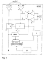
- this data response DQ which is received at input terminal A, read in with a strobe signal DQS DEL (C in FIG. 2), that is to say temporarily stored, which is generated by time delay of the data strobe response signal DQS generated by the memory module DUT to be tested and received at the input terminal B.
- DQS DEL C in FIG. 2
- the data response signal DQ arriving at connection A from the DUT passes through a buffer circuit, for example one Tristate buffer 1 to a data input D of a data latch 2.
- the signal DQ present at the data input D (A in FIG. 2) is in the data latch 2 with one at its set input S applied signal C latched, which from the data strobe response signal DQS (signal at input B) due to delay by a certain delay time ⁇ in a delay device 3 is generated.
- DQ and DQS should be a maximum of ⁇ 500 ps apart may deviate in order to ensure a safe reading at the receiver, for Example of a controller.
- the creates in the Delay device 3 specifically programmed delay time ⁇ a target condition for checking the temporal Position between the data response DQ and to be read in by the DUT the data strobe response signal DQS.
- a reading failure the data response DQ in the latch 2 is namely if a optimal or target time delay ⁇ in the delay device 3 a criterion was set for that the temporal relationship between that received by the DUT Data response DQ and the data strobe response signal DQS at Test is incorrect.
- the circuit arrangement has a calibration signal generator 8 and drivers 9 and 10 as well as a switch arrangement 11, with which a symmetrical clock signal is preferably generated and supplied in a calibration cycle, which on the output side of the buffer amplifiers 9 and 10 is converted into the identical calibration signals DQ KAL (FIG. 2: D ) and DQS KAL (Fig. 2: E) is branched.
- the delay device 3 is programmable via a counter 4.
- a comparator 6 compares whether the data latch 2 has correctly read the calibration signal DQ KAL (D) with the calibration signal DQS KAL, DEL (FIG. 2: F) delayed by the delay time ⁇ in the delay device 3 or not.
- the result of the comparator 6 is stored in a register 7.
- the counter 4 is incremented linearly and the comparison result is stored step by step in the register 7.
- the register contents indicated in FIG. 1 show, by way of example, that a "0" is stored in register 7 if the comparison result of comparator 6 is negative and that "1" is stored if the comparison result of comparator 6 is positive.
- the data for counter positions 3 to 7 are read correctly. This result of the calibration process means that the data eye is hit sufficiently well in this area by the counter reading 3 to 7, ie that the edge of the calibration signal DQS KAL, DEL (F) delayed by the delay time ⁇ in the delay device 3 corresponds to the respective logical value of the calibration signal DQ KAL (D) has latched correctly into latch 2 for the data response.
- 1 contains an evaluation device shown in broken lines 12, which is the calibration result in register 7 evaluates and the counter according to the evaluation result 4 to a central value, in this example the Counter reading "5" for the one following the calibration process real test operation.
- the method and the device can also be used to test the temporal relationships between the real data strobe response signal DQS and the data response DQ.
- the calibration signal in Fig. 1 is 500 MHz.
- 500 MHz corresponds to a cycle time of 2 ns, which means that the calibration signal is 1 ns high and 1 ns low.
- the calibration signal DQ KAL for the data response over five counter positions was read correctly in register 7 in the calibration cycle, one counter position corresponds to a delay of 200 ps.
- the content of the register 7 can thus be evaluated for the temporal relationship between the data response DQ and the data strobe response signal DQS.
- circuit arrangement shown in Fig. 1 the device for reading and checking the temporal position of one to be tested during the test Memory chip, in particular a DRAM in DDR mode, read out data response with the help of a specific Delay time of delayed real data response signal represents only an exemplary principle execution. Numerous circuit realizations of this Principles are possible, for example in one concrete implementation of the buffer amplifier 1, the data latch 2 and the delay device 3 in a single Circuit unit can be realized. To latch the data response DQ two data latches 2 can also be provided be so that each with the rising and falling edge the delayed pending at the set input of data latch 2 Data strobe response signal DQS is latched.
Landscapes
- Dram (AREA)
- For Increasing The Reliability Of Semiconductor Memories (AREA)
- Techniques For Improving Reliability Of Storages (AREA)
Abstract
Description
- Fig. 1
- ein Blockschaltbild eines durch eine BOST-Lösung realisierten Ausführungsbeispiels einer erfindungsgemäßen Vorrichtung mit Mitteln zum Kalibrieren des DQS-Signals und
- Fig. 2
- Signalzeitdiagramme von Signalen A-F an einzelnen Signalleitungen der in Fig. 1 dargestellten Schaltung.
Claims (15)
- Verfahren zum Einlesen und zur Überprüfung der zeitlichen Lage einer beim Test aus einem zu testenden schnellen Speicherbaustein, insbesondere DRAM-Speicher im DDR-Betrieb ausgelesenen Datenantwort (DQ) in einem Testempfänger (BOST),
dadurch gekennzeichnet, daß die Datenantwort (DQ) mit einem Strobesignal (DQSDEL) eingelesen wird, das aus einem vom zu testenden Speicherbaustein (DUT) erzeugten und vom Testempfänger empfangenen Datenstrobe-Antwortsignal (DQS) im Testempfänger (BOST) erzeugt wird. - Verfahren nach Anspruch 1,
dadurch gekennzeichnet, daß das Strobesignal (DQSDEL) durch Zeitverzögerung um eine bestimmte Verzögerungszeit (τ) des im Testempfänger (BOST) empfangenen Datenstrobe-Antwortsignals (DQS) erzeugt wird, wobei die Verzögerungszeit (τ) entsprechend Sollwerten der zeitlichen Lage der vom zu testenden Speicherbaustein (DUT) ausgelesenen Datenantwort (DQ) und des Datenstrobe-Antwortsignals (DQS) ermittelt und eingestellt wird. - Verfahren nach Anspruch 2,
dadurch gekennzeichnet, daß die eingestellte Verzögerungszeit (τ) in eine programmierbare Verzögerungseinrichtung (3) des Testempfängers (BOST) einprogrammiert wird. - Verfahren nach Anspruch 2 oder 3,
dadurch gekennzeichnet, daß zur Ermittlung der Verzögerungszeit (τ) (BOST) ein Kalibriersignal (DQKAL, DQSKAL) für die Datenantwort (DQ) und das Datenstrobe-Antwortsignal (DQS) im Testempfänger erzeugt und den Testsignaleingängen (A, B) für die Datenantwort (DQ) und das Datenstrobe-Antwortsignal (DQS) zugeführt wird. - Verfahren nach einem der Ansprüche 2 oder 3,
dadurch gekennzeichnet, daß zur Ermittlung der in die Verzögerungseinrichtung (3) einzuprogrammierenden Verzögerungszeit (τ ) die Testsignaleingänge (A, B) des Testempfängers (BOST) für die Datenantwort (DQ) und das Datenstrobe-Antwortsignal (DQS) mit einem extern erzeugten Kalibriersignal (DQKAL, DQSKAL) beaufschlagt werden. - Verfahren nach Anspruch 4 oder 5,
dadurch gekennzeichnet, daß die Kalibriersignale (DQKAL, DQSKAL) für die Datenantwort (DQ) und das Datenstrobe-Antwortsignal (DQS) identische Taktsignale sind. - Verfahren nach Anspruch 6,
dadurch gekennzeichnet, daß die Kalibriersignale (DQKAL, DQSKAL) als ein symmetrisches Taktsignal mit einer mit der Frequenz der Datenantwort (DQ) und des Datenstrobe-Antwortsignals (DQS) vom zu testenden Speicherbaustein (DUT) übereinstimmenden Frequenz erzeugt werden. - Verfahren nach einem der vorangehenden Ansprüche,
dadurch gekennzeichnet, daß die vom zu testenden Speicherbaustein einzulesende Datenantwort (DQ) eine Datenantwortsignalgruppe ist, deren Einzelsignale jeweils gleiche zeitliche Sollbeziehung zum vom zu testenden Speicherbaustein erzeugten Datenstrobe-Antwortsignal (DQS) aufweisen. - Verfahren nach einem der vorangehenden Ansprüche,
dadurch gekennzeichnet, daß die ermittelte und in die Verzögerungseinrichtung (3) einzuprogrammierende Verzögerungszeit (τ) als Test-Vergleichswert für die zeitliche Beziehung zwischen der Datenantwort (DQ) und dem Datenstrobe-Antwortsignal (DQS) gespeichert und zum Test dieser dieser zeitlichen Beziehung verwendet wird. - Vorrichtung zum Einlesen und zur Überprüfung der zeitlichen Lage einer beim Test aus einem zu testenden Speicherbaustein (DUT), insbesondere aus einem DRAM-Speicher im DDR-Betrieb ausgelesenen Datenantwort (DQ) in einem Testempfänger (BOST), insbesondere zur Durchführung des Verfahrens nach einem der Ansprüche 1 bis 9,
dadurch gekennzeichnet, daß der Testempfänger (BOST) aufweist:mindestens eine mit einem Testsignaleingang (A) des Testempfängers (BOST) verbundene Latchschaltung (2) zum Speichern der vom zu testenden Speicherbaustein empfangenen Datenantwort (DQ);eine in ihrer Verzögerungszeit (τ) programmierbare Verzögerungseinrichtung (3), die in einem Testzyklus das vom zu testenden Speicherbaustein empfangene Datenstrobe-Antwortsignal (DQS) verzögert und als internes verzögertes Strobesignal (DQSDEL) einem Setzeingang der Latchschaltung (2) zum Einspeichern der anliegenden Datenantwort (DQ) zuführt. - Vorrichtung nach Anspruch 10,
dadurch gekennzeichnet, daß der Testempfänger (BOST) weiterhin aufweist:eine Kalibriereinrichtung (4-12) zur Kalibrierung des Strobesignals (DQSDEL) gegenüber der Datenantwort (DQ) vom zu testenden Speicherbaustein (DUT) in einem Kalibrierzyklus des Testempfängers (BOST), wobei die Kalibriereinrichtung mittels eines den Signaleingängen (A, B) des Testempfängers (BOST) zugeführten Taktsignals (8) und eines durch einen Vergleicher (6) ermittelten Latcherfolgs der Latchschaltung (2) für das der Latchschaltung (2) angelegte Kalibriersignal (DQKAL) einen Wert zur Kalibrierung der Verzögerungszeit (τ) der Verzögerungseinrichtung (3) erzeugt. - Vorrichtung nach Anspruch 11,
dadurch gekennzeichnet, daß die Kalibriereinrichtung (4-12) des Testempfängers (BOST) weiterhin aufweist:einen mit einem Programmiereingang der Verzögerungseinrichtung (3) verbundenen linearen Zähler (4) zum schrittweisen Verändern der Verzögerungszeit (τ) für die Verzögerungseinrichtung (3) im Kalibrierzyklus,eine Registereinheit (7), die, gesteuert vom Zähltakt des Zählers, im Kalibrierzyklus den jeweiligen vom Vergleicher (6) ermittelten Latcherfolg (oder Mißerfolg) der Latchschaltung (2) schrittweise über mehrere Zählerpositionen des Zählers (4) registriert, undeine Auswerteeinrichtung (12), die die von der Registereinheit (7) registrierten Werte hinsichtlich einer optimalen Verzögerungszeit (τ) für die Verzögerungseinrichtung (3) auswertet und den Zähler (4) für die Programmierung der Verzögerungszeit (τ) in der Verzögerungseinrichtung (3) entsprechend für den Testzyklus einstellt. - Vorrichtung nach einem der Ansprüche 10 bis 12,
dadurch gekennzeichnet, daß die Datenantwort (DQ) vom zu testenden Speicherbaustein (DUT) einer Datenantwortsignalgruppe zugehörig ist und daß eine der Anzahl der Datenantwortsignale der Antwortsignalgruppe entsprechende Anzahl von Latchschaltungen (2) im Testempfänger (BOST) vorgesehen sind. - Vorrichtung nach einem der Ansprüche 10 bis 13,
dadurch gekennzeichnet, daß für jedes Datenantwortsignal (DQ) zwei Latchschaltungen (2) jeweils für die Einspeicherung einer steigenden und fallenden Flanke der Datenantwort (DQ) vorgesehen sind. - Vorrichtung nach einem der Ansprüche 10 bis 14,
dadurch gekennzeichnet, daß der Testempfänger (BOST) in einer von einem herkömmlichen Testequipment separaten Halbleiterschaltung (Build Outside Self Test) implementiert ist, die in unmittelbarer Nähe des jeweiligen zu testenden Speicherbausteins (DUT), insbesondere DRAM-Speichers, angeordnet ist.
Applications Claiming Priority (2)
| Application Number | Priority Date | Filing Date | Title |
|---|---|---|---|
| DE10034852 | 2000-07-18 | ||
| DE10034852A DE10034852A1 (de) | 2000-07-18 | 2000-07-18 | Verfahren und Vorrichtung zum Einlesen und zur Überprüfung der zeitlichen Lage von aus einem zu testenden Speicherbaustein ausgelesenen Datenantwortsignalen |
Publications (3)
| Publication Number | Publication Date |
|---|---|
| EP1176606A2 true EP1176606A2 (de) | 2002-01-30 |
| EP1176606A3 EP1176606A3 (de) | 2006-05-10 |
| EP1176606B1 EP1176606B1 (de) | 2010-03-03 |
Family
ID=7649289
Family Applications (1)
| Application Number | Title | Priority Date | Filing Date |
|---|---|---|---|
| EP01115502A Expired - Lifetime EP1176606B1 (de) | 2000-07-18 | 2001-06-27 | Verfahren und Vorrichtung zum Einlesen und zur Überprüfung der zeitlichen Lage von aus einem zu testenden Speicherbaustein ausgelesenen Datenantwortsignalen |
Country Status (4)
| Country | Link |
|---|---|
| US (1) | US6871306B2 (de) |
| EP (1) | EP1176606B1 (de) |
| DE (2) | DE10034852A1 (de) |
| TW (1) | TW583679B (de) |
Families Citing this family (17)
| Publication number | Priority date | Publication date | Assignee | Title |
|---|---|---|---|---|
| US6889334B1 (en) * | 2001-10-02 | 2005-05-03 | Advanced Micro Devices, Inc. | Multimode system for calibrating a data strobe delay for a memory read operation |
| US6990644B2 (en) * | 2002-04-18 | 2006-01-24 | International Business Machines Corporation | On chip timing adjustment in multi-channel fast data transfer |
| DE10231419B4 (de) * | 2002-07-11 | 2015-01-29 | Qimonda Ag | Vorrichtung und Verfahren zur Kalibrierung von Signalen |
| DE10340917B4 (de) * | 2003-09-05 | 2012-03-22 | Qimonda Ag | Verfahren und Vorrichtung zum Überprüfen von Ausgangssignalen einer integrierten Schaltung |
| KR100582391B1 (ko) * | 2004-04-08 | 2006-05-22 | 주식회사 하이닉스반도체 | 반도체 소자에서의 지연 요소의 지연 검출 장치 및 방법 |
| DE102004020030A1 (de) * | 2004-04-23 | 2005-11-24 | Infineon Technologies Ag | Testvorrichtung zum Testen einer integrierten Schaltung |
| DE102004020867A1 (de) * | 2004-04-28 | 2005-11-24 | Infineon Technologies Ag | Halbleiter-Bauelement-Test-Verfahren, sowie Daten-Zwischenspeicher-Bauelement |
| DE102004020866A1 (de) * | 2004-04-28 | 2005-11-24 | Infineon Technologies Ag | Halbleiter-Bauelement-Test-Verfahren, sowie Daten-Zwischenspeicher-Bauelement |
| DE102004036145A1 (de) * | 2004-07-26 | 2006-03-23 | Infineon Technologies Ag | Halbleiterschaltungseinrichtung und System zum Testen einer Halbleitervorrichtung |
| US7164289B1 (en) | 2005-01-21 | 2007-01-16 | Altera Corporation | Real time feedback compensation of programmable logic memory |
| DE102005051996A1 (de) * | 2005-10-31 | 2007-05-03 | Infineon Technologies Ag | Leseverstärker |
| JP4957092B2 (ja) * | 2006-06-26 | 2012-06-20 | 横河電機株式会社 | 半導体メモリテスタ |
| KR100891326B1 (ko) * | 2006-07-31 | 2009-03-31 | 삼성전자주식회사 | 반도체 메모리 장치의 내부 클럭 신호를 데이터 스트로브신호로서 이용하는 반도체 메모리 장치의 테스트 방법 및테스트 시스템 |
| US7715251B2 (en) * | 2006-10-25 | 2010-05-11 | Hewlett-Packard Development Company, L.P. | Memory access strobe configuration system and process |
| US8307270B2 (en) | 2009-09-03 | 2012-11-06 | International Business Machines Corporation | Advanced memory device having improved performance, reduced power and increased reliability |
| US9454421B2 (en) * | 2013-10-15 | 2016-09-27 | Cypress Semiconductor Corporation | Method for providing read data flow control or error reporting using a read data strobe |
| CN116665731B (zh) * | 2023-08-02 | 2023-10-03 | 成都智多晶科技有限公司 | 一种ddr存储器采样校准方法及ddr存储器 |
Family Cites Families (10)
| Publication number | Priority date | Publication date | Assignee | Title |
|---|---|---|---|---|
| JPS6378400A (ja) * | 1986-09-19 | 1988-04-08 | Fujitsu Ltd | Ram試験方式 |
| US6587978B1 (en) * | 1994-02-14 | 2003-07-01 | Micron Technology, Inc. | Circuit and method for varying a pulse width of an internal control signal during a test mode |
| US6142683A (en) * | 1997-04-08 | 2000-11-07 | Advanced Micro Devices, Inc. | Debug interface including data steering between a processor, an input/output port, and a trace logic |
| US6067651A (en) * | 1998-02-20 | 2000-05-23 | Hewlett-Packard Company | Test pattern generator having improved test sequence compaction |
| JP2000076853A (ja) * | 1998-06-17 | 2000-03-14 | Mitsubishi Electric Corp | 同期型半導体記憶装置 |
| JP2000021193A (ja) * | 1998-07-01 | 2000-01-21 | Fujitsu Ltd | メモリ試験方法及び装置並びに記憶媒体 |
| US6671836B1 (en) * | 1999-09-23 | 2003-12-30 | Rambus Inc. | Method and apparatus for testing memory |
| DE10034899C1 (de) * | 2000-07-18 | 2002-07-04 | Infineon Technologies Ag | System zum Test schneller synchroner Halbleiterschaltungen |
| DE10034855B4 (de) * | 2000-07-18 | 2006-05-11 | Infineon Technologies Ag | System zum Test von schnellen integrierten Digitalschaltungen und BOST-Halbleiterschaltungsbaustein als Testschaltkreis |
| GB0026849D0 (en) * | 2000-11-03 | 2000-12-20 | Acuid Corp Ltd | DDR SDRAM memory test system with fault strobe synchronization |
-
2000
- 2000-07-18 DE DE10034852A patent/DE10034852A1/de not_active Withdrawn
-
2001
- 2001-06-27 EP EP01115502A patent/EP1176606B1/de not_active Expired - Lifetime
- 2001-06-27 DE DE50115368T patent/DE50115368D1/de not_active Expired - Lifetime
- 2001-07-17 TW TW090117427A patent/TW583679B/zh not_active IP Right Cessation
- 2001-07-18 US US09/907,692 patent/US6871306B2/en not_active Expired - Lifetime
Also Published As
| Publication number | Publication date |
|---|---|
| DE50115368D1 (de) | 2010-04-15 |
| US6871306B2 (en) | 2005-03-22 |
| TW583679B (en) | 2004-04-11 |
| EP1176606B1 (de) | 2010-03-03 |
| US20020160558A1 (en) | 2002-10-31 |
| EP1176606A3 (de) | 2006-05-10 |
| DE10034852A1 (de) | 2002-02-07 |
Similar Documents
| Publication | Publication Date | Title |
|---|---|---|
| EP1176606B1 (de) | Verfahren und Vorrichtung zum Einlesen und zur Überprüfung der zeitlichen Lage von aus einem zu testenden Speicherbaustein ausgelesenen Datenantwortsignalen | |
| DE3587223T2 (de) | Unabhängige Matrixtaktierung. | |
| DE60204597T2 (de) | Kompakter automatischer tester (ate) mit zeitstempel-system | |
| DE19915398B4 (de) | Verfahren zum Einstellen von Verzögerungszeiten einer Mehrzahl von Anschlusskarten in einem IC-Testgerät | |
| DE69506337T2 (de) | Von einem LSI-Prüfer mit einer verminderten Anzahl von Stiften testbare integrierte Halbleiterschaltung | |
| DE10034899C1 (de) | System zum Test schneller synchroner Halbleiterschaltungen | |
| DE3788586T2 (de) | Schaltung zur Prüfung des Eingangsspannungssignals für eine halbleiterintegrierte Schaltung. | |
| DE10101899A1 (de) | Verfahren und Vorrichtung zum Testen von Halbleiterbauelementen | |
| DE3781229T2 (de) | Pruefsystem fuer direktzugriffsspeicher. | |
| DE112005001517B4 (de) | Synchronisation zwischen Niedrigfrequenz- und Hochfrequenzdigitalsignalen | |
| DE60307297T2 (de) | Verfahren und einrichtung zur ruhestrombestimmung | |
| DE10113458C2 (de) | Testschaltung | |
| DE10141025B4 (de) | Verfahren zum Testen von Wafern unter Verwendung eines Kalibrierwafers und zugehöriger Kalibriewafer | |
| EP1176607A2 (de) | Verfahrenund Vorrichtung zum Testen von Setup-Zeit und Hold-Zeit von Signalen einer Schaltung mit getakteter Datenübertragung | |
| DE10219916A1 (de) | Testanordnung mit Testautomat und integriertem Schaltkreis sowie Verfahren zur Ermittlung des Zeitverhaltens eines integrierten Schaltkreises | |
| DE10121309B4 (de) | Testschaltung zum Testen einer zu testenden Schaltung | |
| DE102008013099A1 (de) | Speichertestschaltung | |
| DE10231419B4 (de) | Vorrichtung und Verfahren zur Kalibrierung von Signalen | |
| DE10392393T5 (de) | Halbleiterprüfvorrichtung und Zeitmessverfahren hierfür | |
| DE10006236C2 (de) | Anordnung zum Generieren von Signalimpulsen mit definierten Pulslängen in einem Baustein mit BIST-Funktion | |
| EP1390951B1 (de) | Dynamischer speicher und verfahren zum testen eines dynamischen speichers | |
| DE10062081A1 (de) | Integrierte Halbleiterschaltung und Verfahren zum Testen der integrierten Halbleiterschaltung | |
| DE102007001023A1 (de) | Spannungsüberwachungseinrichtung in einer Halbleiterspeichereinrichtung | |
| EP3701276B1 (de) | Integrierte schaltung und asic | |
| DE10340917B4 (de) | Verfahren und Vorrichtung zum Überprüfen von Ausgangssignalen einer integrierten Schaltung |
Legal Events
| Date | Code | Title | Description |
|---|---|---|---|
| PUAI | Public reference made under article 153(3) epc to a published international application that has entered the european phase |
Free format text: ORIGINAL CODE: 0009012 |
|
| AK | Designated contracting states |
Kind code of ref document: A2 Designated state(s): AT BE CH CY DE DK ES FI FR GB GR IE IT LI LU MC NL PT SE TR |
|
| AX | Request for extension of the european patent |
Free format text: AL;LT;LV;MK;RO;SI |
|
| PUAL | Search report despatched |
Free format text: ORIGINAL CODE: 0009013 |
|
| AK | Designated contracting states |
Kind code of ref document: A3 Designated state(s): AT BE CH CY DE DK ES FI FR GB GR IE IT LI LU MC NL PT SE TR |
|
| AX | Request for extension of the european patent |
Extension state: AL LT LV MK RO SI |
|
| RAP1 | Party data changed (applicant data changed or rights of an application transferred) |
Owner name: QIMONDA AG |
|
| 17P | Request for examination filed |
Effective date: 20061011 |
|
| 17Q | First examination report despatched |
Effective date: 20061123 |
|
| AKX | Designation fees paid |
Designated state(s): DE GB IE |
|
| GRAP | Despatch of communication of intention to grant a patent |
Free format text: ORIGINAL CODE: EPIDOSNIGR1 |
|
| GRAS | Grant fee paid |
Free format text: ORIGINAL CODE: EPIDOSNIGR3 |
|
| 19U | Interruption of proceedings before grant |
Effective date: 20090401 |
|
| 19W | Proceedings resumed before grant after interruption of proceedings |
Effective date: 20091123 |
|
| GRAA | (expected) grant |
Free format text: ORIGINAL CODE: 0009210 |
|
| AK | Designated contracting states |
Kind code of ref document: B1 Designated state(s): DE GB IE |
|
| REG | Reference to a national code |
Ref country code: GB Ref legal event code: FG4D Free format text: NOT ENGLISH |
|
| REG | Reference to a national code |
Ref country code: IE Ref legal event code: FG4D |
|
| REF | Corresponds to: |
Ref document number: 50115368 Country of ref document: DE Date of ref document: 20100415 Kind code of ref document: P |
|
| REG | Reference to a national code |
Ref country code: IE Ref legal event code: FD4D |
|
| PG25 | Lapsed in a contracting state [announced via postgrant information from national office to epo] |
Ref country code: IE Free format text: LAPSE BECAUSE OF FAILURE TO SUBMIT A TRANSLATION OF THE DESCRIPTION OR TO PAY THE FEE WITHIN THE PRESCRIBED TIME-LIMIT Effective date: 20100303 |
|
| PLBE | No opposition filed within time limit |
Free format text: ORIGINAL CODE: 0009261 |
|
| STAA | Information on the status of an ep patent application or granted ep patent |
Free format text: STATUS: NO OPPOSITION FILED WITHIN TIME LIMIT |
|
| 26N | No opposition filed |
Effective date: 20101206 |
|
| REG | Reference to a national code |
Ref country code: DE Ref legal event code: R008 Ref document number: 50115368 Country of ref document: DE |
|
| REG | Reference to a national code |
Ref country code: DE Ref legal event code: R039 Ref document number: 50115368 Country of ref document: DE Effective date: 20121005 |
|
| REG | Reference to a national code |
Ref country code: DE Ref legal event code: R040 Ref document number: 50115368 Country of ref document: DE Ref country code: DE Ref legal event code: R097 Ref document number: 50115368 Country of ref document: DE |
|
| REG | Reference to a national code |
Ref country code: DE Ref legal event code: R082 Ref document number: 50115368 Country of ref document: DE |
|
| REG | Reference to a national code |
Ref country code: DE Ref legal event code: R081 Ref document number: 50115368 Country of ref document: DE Owner name: INFINEON TECHNOLOGIES AG, DE Free format text: FORMER OWNER: QIMONDA AG, 81739 MUENCHEN, DE Effective date: 20141117 Ref country code: DE Ref legal event code: R081 Ref document number: 50115368 Country of ref document: DE Owner name: POLARIS INNOVATIONS LTD., IE Free format text: FORMER OWNER: QIMONDA AG, 81739 MUENCHEN, DE Effective date: 20141117 |
|
| REG | Reference to a national code |
Ref country code: DE Ref legal event code: R040 Ref document number: 50115368 Country of ref document: DE Effective date: 20141013 |
|
| REG | Reference to a national code |
Ref country code: GB Ref legal event code: 732E Free format text: REGISTERED BETWEEN 20150827 AND 20150902 |
|
| REG | Reference to a national code |
Ref country code: DE Ref legal event code: R081 Ref document number: 50115368 Country of ref document: DE Owner name: POLARIS INNOVATIONS LTD., IE Free format text: FORMER OWNER: INFINEON TECHNOLOGIES AG, 85579 NEUBIBERG, DE |
|
| PGFP | Annual fee paid to national office [announced via postgrant information from national office to epo] |
Ref country code: GB Payment date: 20160622 Year of fee payment: 16 |
|
| GBPC | Gb: european patent ceased through non-payment of renewal fee |
Effective date: 20170627 |
|
| PG25 | Lapsed in a contracting state [announced via postgrant information from national office to epo] |
Ref country code: GB Free format text: LAPSE BECAUSE OF NON-PAYMENT OF DUE FEES Effective date: 20170627 |
|
| PGFP | Annual fee paid to national office [announced via postgrant information from national office to epo] |
Ref country code: DE Payment date: 20200617 Year of fee payment: 20 |
|
| REG | Reference to a national code |
Ref country code: DE Ref legal event code: R071 Ref document number: 50115368 Country of ref document: DE |