EP1176604A2 - Verfahren zum Testen einer Vielzahl von Wortleitungen einer Halbleiterspeicheranordnung - Google Patents
Verfahren zum Testen einer Vielzahl von Wortleitungen einer Halbleiterspeicheranordnung Download PDFInfo
- Publication number
- EP1176604A2 EP1176604A2 EP01111474A EP01111474A EP1176604A2 EP 1176604 A2 EP1176604 A2 EP 1176604A2 EP 01111474 A EP01111474 A EP 01111474A EP 01111474 A EP01111474 A EP 01111474A EP 1176604 A2 EP1176604 A2 EP 1176604A2
- Authority
- EP
- European Patent Office
- Prior art keywords
- word lines
- potential
- vnwl
- active
- negative
- Prior art date
- Legal status (The legal status is an assumption and is not a legal conclusion. Google has not performed a legal analysis and makes no representation as to the accuracy of the status listed.)
- Granted
Links
- 238000012360 testing method Methods 0.000 title claims abstract description 17
- 238000000034 method Methods 0.000 title claims abstract description 13
- 239000004065 semiconductor Substances 0.000 title claims abstract description 12
- 230000014759 maintenance of location Effects 0.000 description 4
- 230000005669 field effect Effects 0.000 description 3
- 238000003491 array Methods 0.000 description 2
- 230000000295 complement effect Effects 0.000 description 1
- 230000008878 coupling Effects 0.000 description 1
- 238000010168 coupling process Methods 0.000 description 1
- 238000005859 coupling reaction Methods 0.000 description 1
- 238000010586 diagram Methods 0.000 description 1
Images
Classifications
-
- G—PHYSICS
- G11—INFORMATION STORAGE
- G11C—STATIC STORES
- G11C29/00—Checking stores for correct operation ; Subsequent repair; Testing stores during standby or offline operation
-
- G—PHYSICS
- G11—INFORMATION STORAGE
- G11C—STATIC STORES
- G11C29/00—Checking stores for correct operation ; Subsequent repair; Testing stores during standby or offline operation
- G11C29/04—Detection or location of defective memory elements, e.g. cell constructio details, timing of test signals
- G11C29/08—Functional testing, e.g. testing during refresh, power-on self testing [POST] or distributed testing
- G11C29/12—Built-in arrangements for testing, e.g. built-in self testing [BIST] or interconnection details
- G11C29/18—Address generation devices; Devices for accessing memories, e.g. details of addressing circuits
- G11C29/26—Accessing multiple arrays
Definitions
- the present invention relates to a method for testing a plurality of word lines of a semiconductor memory device in a multiple word line (WL) wafer test, at several word lines initially at a high potential booted up and activated so that the active word lines started up to a negative VNWL potential to be shut down.
- WL word line
- inactive word lines that is to say word lines that are not activated for writing or reading a memory cell, do not become ground or ground potential as before 0 V, but brought to a slightly negative word line voltage VNWL of about -0.3 V.
- This negative word line voltage VNWL is provided in the semiconductor memory arrangement by a generator dedicated to this.
- VNWL becomes the reverse current of the selection transistors of the individual memory cells reduced what makes these transistors hold data longer. In other words, the negative word line voltage leads to an improvement the data retention or retention time.
- This task is carried out in a method of the aforementioned Art solved according to the invention in that the not started and thus inactive word lines before shutdown of the active word lines with high resistance on the negative VNWL potential float and that after shutting down the active word lines all word lines again with the negative VNWL potential can be connected.
- the inactive Word lines shortly before shutting down the active word lines in the multiple WL wafer test not with the negative VNWL potential connected. Rather, they become inactive Word lines with high resistance at the negative VNWL potential to Brought float. Only when all word lines shut down are also all word lines with the negative VNWL potential connected.
- the inventive method is in without major changes the existing semiconductor memory arrays on simple Realizable way: it is only necessary the logic of wordline drivers that deliver the VNWL potential, adapt accordingly to the above procedure or the generator that provides the VNWL potential, to design stronger, but this requires additional chip area.
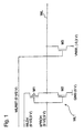
- a word line WL is from a word line driver WLT complementary field-effect transistors M1, M2 connected, which in series between ground potential GND and a word line drive voltage WLDV of 0 V or 2.9 V and via a precharge voltage bPRCH of also 0 V or 2.9 V are controlled.
- a field effect transistor M3 lies between the word line WL and the negative VNWL potential of -0.3 V and is via a word line reset signal WLRST of 0 V or 2 V can be controlled.
- the word line WL is over the Word line driver WLT with transistor M3 switched off Started up 2.9 V and then shut down again to 0 V.
- the word line WL shown is an inactive word line and are other word lines of the memory cell array, not shown switched to active, the word line WL is initially with the field effect transistor M3 switched on VNWL potential of -0.3 V. Just before shutting down the active word lines, the word line WL becomes high-impedance brought the VNWL potential to float. For this, a corresponding WLRST signal applied to transistor M3 in order turn it off. With the word line driver also switched off WLT then floats the inactive word line WL high impedance at the VNWL potential of -0.3 V.
Landscapes
- For Increasing The Reliability Of Semiconductor Memories (AREA)
- Tests Of Electronic Circuits (AREA)
- Dram (AREA)
- Semiconductor Memories (AREA)
Abstract
Description
Claims (4)
- Verfahren zum Testen einer Vielzahl von Wortleitungen (WL) einer Halbleiterspeicheranordnung bei einem Multiple-WL-Wafertest, bei dem mehrere Wortleitungen (WL) zunächst auf ein hohes Potential hochgefahren und so aktiv geschaltet werden und bei dem die so hochgefahrenen aktiven Wortleitungen (WL) sodann auf ein niedriges Potential heruntergefahren werden,
dadurch gekennzeichnet, daß
die nicht hochgefahrenen und damit inaktiven Wortleitungen vor dem Herunterfahren der aktiven Wortleitungen (WL) hochohmig auf einem negativen VNWL-Potential floaten und daß nach dem Herunterfahren der aktiven Wortleitungen alle Wortleitungen wieder mit dem negativen VNWL-Potential verbunden werden. - Verfahren nach Anspruch 1,
dadurch gekennzeichnet, daß
die inaktiven Wortleitungen vor dem Herunterfahren der aktiven Wortleitungen mit dem negativen VNWL-Potential verbunden sind. - Verfahren nach Anspruch 1 oder 2,
dadurch gekennzeichnet, daß
für das VNWL-Potential ein Potential von etwa -0,3 V verwendet wird. - Verfahren nach einem der Ansprüche 1 bis 3,
dadurch gekennzeichnet, daß
das negative VNWL-Potential über einen Transistor (M3) an die Wortleitung (WL) gelegt wird.
Applications Claiming Priority (2)
| Application Number | Priority Date | Filing Date | Title |
|---|---|---|---|
| DE10026275 | 2000-05-26 | ||
| DE10026275A DE10026275A1 (de) | 2000-05-26 | 2000-05-26 | Verfahren zum Testen einer Vielzahl von Wortleitungen einer Halbleiterspeicheranordnung |
Publications (3)
| Publication Number | Publication Date |
|---|---|
| EP1176604A2 true EP1176604A2 (de) | 2002-01-30 |
| EP1176604A3 EP1176604A3 (de) | 2002-05-29 |
| EP1176604B1 EP1176604B1 (de) | 2007-01-03 |
Family
ID=7643756
Family Applications (1)
| Application Number | Title | Priority Date | Filing Date |
|---|---|---|---|
| EP01111474A Expired - Lifetime EP1176604B1 (de) | 2000-05-26 | 2001-05-10 | Verfahren zum Testen einer Vielzahl von Wortleitungen einer Halbleiterspeicheranordnung |
Country Status (6)
| Country | Link |
|---|---|
| US (1) | US6370069B2 (de) |
| EP (1) | EP1176604B1 (de) |
| JP (1) | JP3611203B2 (de) |
| KR (1) | KR100409122B1 (de) |
| DE (2) | DE10026275A1 (de) |
| TW (1) | TW559820B (de) |
Families Citing this family (11)
| Publication number | Priority date | Publication date | Assignee | Title |
|---|---|---|---|---|
| JP4245147B2 (ja) | 2003-10-28 | 2009-03-25 | エルピーダメモリ株式会社 | 階層ワード線方式の半導体記憶装置と、それに使用されるサブワードドライバ回路 |
| US7245548B2 (en) * | 2004-07-27 | 2007-07-17 | Micron Technology, Inc. | Techniques for reducing leakage current in memory devices |
| US7286417B2 (en) * | 2005-06-21 | 2007-10-23 | Micron Technology, Inc. | Low power dissipation voltage generator |
| US7313033B2 (en) * | 2005-09-28 | 2007-12-25 | Infineon Technologies Ag | Random access memory including first and second voltage sources |
| JP5029205B2 (ja) * | 2007-08-10 | 2012-09-19 | 富士通セミコンダクター株式会社 | 半導体メモリ、半導体メモリのテスト方法およびシステム |
| US8605525B2 (en) * | 2010-11-23 | 2013-12-10 | Macronix International Co., Ltd. | System and method for testing for defects in a semiconductor memory array |
| CN102568578A (zh) * | 2010-12-08 | 2012-07-11 | 旺宏电子股份有限公司 | 半导体存储装置及其测试及控制方法 |
| US9503091B2 (en) * | 2013-11-20 | 2016-11-22 | Globalfoundries Inc. | Wordline decoder circuits for embedded charge trap multi-time-programmable-read-only-memory |
| JP2015170379A (ja) * | 2014-03-10 | 2015-09-28 | マイクロン テクノロジー, インク. | 半導体装置 |
| TWI852168B (zh) * | 2022-11-16 | 2024-08-11 | 立積電子股份有限公司 | 開關裝置 |
| TWI865988B (zh) | 2022-12-14 | 2024-12-11 | 立積電子股份有限公司 | 開關裝置 |
Family Cites Families (10)
| Publication number | Priority date | Publication date | Assignee | Title |
|---|---|---|---|---|
| US4751679A (en) * | 1986-12-22 | 1988-06-14 | Motorola, Inc. | Gate stress test of a MOS memory |
| JPH0760845B2 (ja) * | 1991-03-22 | 1995-06-28 | 株式会社東芝 | 半導体記憶装置 |
| KR950009204B1 (ko) * | 1993-04-08 | 1995-08-16 | 삼성전자 주식회사 | 반도체 집적회로의 워드라인 드라이버회로 및 그 소오스전원 공급방법 |
| JP3667787B2 (ja) * | 1994-05-11 | 2005-07-06 | 株式会社ルネサステクノロジ | 半導体記憶装置 |
| KR0135108B1 (ko) * | 1994-12-13 | 1998-04-25 | 김광호 | 스트레스 테스트 회로를 포함하는 반도체 메모리 장치 |
| JP3712150B2 (ja) * | 1996-10-25 | 2005-11-02 | 株式会社日立製作所 | 半導体集積回路装置 |
| JPH1166874A (ja) * | 1997-08-08 | 1999-03-09 | Mitsubishi Electric Corp | 不揮発性半導体記憶装置 |
| US6016281A (en) * | 1997-12-17 | 2000-01-18 | Siemens Aktiengesellschaft | Memory with word line voltage control |
| KR100269319B1 (ko) * | 1997-12-29 | 2000-10-16 | 윤종용 | 동시칼럼선택라인활성화회로를구비하는반도체메모리장치및칼럼선택라인제어방법 |
| US6049495A (en) * | 1999-02-03 | 2000-04-11 | International Business Machines Corporation | Auto-programmable current limiter to control current leakage due to bitline to wordline short |
-
2000
- 2000-05-26 DE DE10026275A patent/DE10026275A1/de not_active Ceased
-
2001
- 2001-05-10 EP EP01111474A patent/EP1176604B1/de not_active Expired - Lifetime
- 2001-05-10 DE DE50111772T patent/DE50111772D1/de not_active Expired - Fee Related
- 2001-05-25 KR KR10-2001-0028910A patent/KR100409122B1/ko not_active Expired - Fee Related
- 2001-05-25 JP JP2001157851A patent/JP3611203B2/ja not_active Expired - Fee Related
- 2001-05-25 TW TW090112628A patent/TW559820B/zh not_active IP Right Cessation
- 2001-05-29 US US09/867,254 patent/US6370069B2/en not_active Expired - Lifetime
Also Published As
| Publication number | Publication date |
|---|---|
| KR100409122B1 (ko) | 2003-12-06 |
| DE10026275A1 (de) | 2001-12-13 |
| TW559820B (en) | 2003-11-01 |
| EP1176604B1 (de) | 2007-01-03 |
| DE50111772D1 (de) | 2007-02-15 |
| JP3611203B2 (ja) | 2005-01-19 |
| EP1176604A3 (de) | 2002-05-29 |
| JP2002063800A (ja) | 2002-02-28 |
| KR20010107755A (ko) | 2001-12-07 |
| US20010048621A1 (en) | 2001-12-06 |
| US6370069B2 (en) | 2002-04-09 |
Similar Documents
| Publication | Publication Date | Title |
|---|---|---|
| DE3588042T2 (de) | Dynamischer Halbleiterspeicher mit einer statischen Datenspeicherzelle. | |
| DE69227232T2 (de) | Halbleiterspeicher und dessen Siebtestverfahren | |
| DE69129138T2 (de) | DRAM mit einem Wortleitungsbetriebsschaltungssystem | |
| DE69325838T2 (de) | Halbleiter-FIFO-Speicher | |
| DE69221005T2 (de) | Dynamische RAM-Einrichtung mit einem Selektor für mehrere Wortleitungen, der bei einem Einbrenntest verwendet wird | |
| DE69323681T2 (de) | Stressprüfung für Speichernetzwerke in integrierten Schaltungen | |
| DE19508680C2 (de) | Integrierter Halbleiterschaltkreis und Verfahren zum Durchführen eines Belastungstests | |
| DE112018003001T5 (de) | Ferroelektrische 2T1C-Direktzugriffsspeicherzelle | |
| DE102012104648A1 (de) | Techniken zur Verifikation einer Verlässlichkeit eines Speichers | |
| DE102013214258A1 (de) | Vorrichtung mit mehreren statischen Direktzugriffsspeicherzellen und Verfahren zu ihrem Betrieb | |
| DE2650574B2 (de) | Halbleiter-Speicher | |
| EP1176604A2 (de) | Verfahren zum Testen einer Vielzahl von Wortleitungen einer Halbleiterspeicheranordnung | |
| DE10135065B4 (de) | Halbleiterspeichervorrichtung und Verfahren für den Zugriff auf eine Speicherzelle | |
| DE69909202T2 (de) | Anordnung und Verfahren für statischen RAMspeicher | |
| DE102019200314A1 (de) | Schreibunterstützung | |
| DE19832960A1 (de) | Halbleiterspeichervorrichtung mit Einbrenntestfunktion | |
| DE69119732T2 (de) | Dynamischer RAM | |
| DE69126912T2 (de) | Halbleiteranordnung und ihre Prüfungsverfahren | |
| DE10223711A1 (de) | Ferroelektrischer Speicher und Verfahren zu dessen Ansteuerung | |
| DE69228522T2 (de) | Lese-Schreibspeicher mit Prüfmodusdatenvergleich | |
| DE3939849A1 (de) | Halbleiterspeichereinrichtung mit einem geteilten leseverstaerker und verfahren zu deren betrieb | |
| DE102019211875B4 (de) | Spaltenabhängiger positiver Spannungsboost für eine Speicherzellenversorgungsspannung | |
| DE19963417A1 (de) | Nichtflüchtiger ferroelektrischer Speicher | |
| DE10165025B4 (de) | Halbleiterspeicherbauelement mit Subwortleitungstreibern | |
| DE69421480T2 (de) | Halbleiterspeicheranordnung und Betriebsverfahren dafür |
Legal Events
| Date | Code | Title | Description |
|---|---|---|---|
| PUAI | Public reference made under article 153(3) epc to a published international application that has entered the european phase |
Free format text: ORIGINAL CODE: 0009012 |
|
| AK | Designated contracting states |
Kind code of ref document: A2 Designated state(s): AT BE CH CY DE DK ES FI FR GB GR IE IT LI LU MC NL PT SE TR |
|
| AX | Request for extension of the european patent |
Free format text: AL;LT;LV;MK;RO;SI |
|
| PUAL | Search report despatched |
Free format text: ORIGINAL CODE: 0009013 |
|
| AK | Designated contracting states |
Kind code of ref document: A3 Designated state(s): AT BE CH CY DE DK ES FI FR GB GR IE IT LI LU MC NL PT SE TR |
|
| AX | Request for extension of the european patent |
Free format text: AL;LT;LV;MK;RO;SI |
|
| 17P | Request for examination filed |
Effective date: 20021105 |
|
| AKX | Designation fees paid |
Designated state(s): DE GB IE |
|
| GRAP | Despatch of communication of intention to grant a patent |
Free format text: ORIGINAL CODE: EPIDOSNIGR1 |
|
| GRAS | Grant fee paid |
Free format text: ORIGINAL CODE: EPIDOSNIGR3 |
|
| GRAA | (expected) grant |
Free format text: ORIGINAL CODE: 0009210 |
|
| AK | Designated contracting states |
Kind code of ref document: B1 Designated state(s): DE GB IE |
|
| PG25 | Lapsed in a contracting state [announced via postgrant information from national office to epo] |
Ref country code: IE Free format text: LAPSE BECAUSE OF FAILURE TO SUBMIT A TRANSLATION OF THE DESCRIPTION OR TO PAY THE FEE WITHIN THE PRESCRIBED TIME-LIMIT Effective date: 20070103 |
|
| REG | Reference to a national code |
Ref country code: GB Ref legal event code: FG4D Free format text: NOT ENGLISH |
|
| REF | Corresponds to: |
Ref document number: 50111772 Country of ref document: DE Date of ref document: 20070215 Kind code of ref document: P |
|
| REG | Reference to a national code |
Ref country code: IE Ref legal event code: FG4D Free format text: LANGUAGE OF EP DOCUMENT: GERMAN |
|
| GBV | Gb: ep patent (uk) treated as always having been void in accordance with gb section 77(7)/1977 [no translation filed] |
Effective date: 20070103 |
|
| REG | Reference to a national code |
Ref country code: IE Ref legal event code: FD4D |
|
| PLBE | No opposition filed within time limit |
Free format text: ORIGINAL CODE: 0009261 |
|
| STAA | Information on the status of an ep patent application or granted ep patent |
Free format text: STATUS: NO OPPOSITION FILED WITHIN TIME LIMIT |
|
| PG25 | Lapsed in a contracting state [announced via postgrant information from national office to epo] |
Ref country code: GB Free format text: LAPSE BECAUSE OF FAILURE TO SUBMIT A TRANSLATION OF THE DESCRIPTION OR TO PAY THE FEE WITHIN THE PRESCRIBED TIME-LIMIT Effective date: 20070103 |
|
| 26N | No opposition filed |
Effective date: 20071005 |
|
| PGFP | Annual fee paid to national office [announced via postgrant information from national office to epo] |
Ref country code: DE Payment date: 20080715 Year of fee payment: 8 |
|
| PG25 | Lapsed in a contracting state [announced via postgrant information from national office to epo] |
Ref country code: DE Free format text: LAPSE BECAUSE OF NON-PAYMENT OF DUE FEES Effective date: 20091201 |