EP1170804A2 - Grabenkondensator mit Isolationskragen und entsprechendes Herstellungsverfahren - Google Patents
Grabenkondensator mit Isolationskragen und entsprechendes Herstellungsverfahren Download PDFInfo
- Publication number
- EP1170804A2 EP1170804A2 EP01115516A EP01115516A EP1170804A2 EP 1170804 A2 EP1170804 A2 EP 1170804A2 EP 01115516 A EP01115516 A EP 01115516A EP 01115516 A EP01115516 A EP 01115516A EP 1170804 A2 EP1170804 A2 EP 1170804A2
- Authority
- EP
- European Patent Office
- Prior art keywords
- trench
- capacitor
- metal electrode
- electrode layer
- region
- Prior art date
- Legal status (The legal status is an assumption and is not a legal conclusion. Google has not performed a legal analysis and makes no representation as to the accuracy of the status listed.)
- Granted
Links
Images













Classifications
-
- H—ELECTRICITY
- H10—SEMICONDUCTOR DEVICES; ELECTRIC SOLID-STATE DEVICES NOT OTHERWISE PROVIDED FOR
- H10B—ELECTRONIC MEMORY DEVICES
- H10B12/00—Dynamic random access memory [DRAM] devices
- H10B12/01—Manufacture or treatment
- H10B12/02—Manufacture or treatment for one transistor one-capacitor [1T-1C] memory cells
- H10B12/03—Making the capacitor or connections thereto
- H10B12/038—Making the capacitor or connections thereto the capacitor being in a trench in the substrate
-
- H—ELECTRICITY
- H10—SEMICONDUCTOR DEVICES; ELECTRIC SOLID-STATE DEVICES NOT OTHERWISE PROVIDED FOR
- H10D—INORGANIC ELECTRIC SEMICONDUCTOR DEVICES
- H10D1/00—Resistors, capacitors or inductors
- H10D1/60—Capacitors
- H10D1/62—Capacitors having potential barriers
- H10D1/66—Conductor-insulator-semiconductor capacitors, e.g. MOS capacitors
- H10D1/665—Trench conductor-insulator-semiconductor capacitors, e.g. trench MOS capacitors
Definitions
- the present invention relates to a trench capacitor, especially for use in a semiconductor memory cell, with a trench formed in a semiconductor substrate is; one in the trench first and second conductive capacitor plate; one between the first and second capacitor plate located dielectric layer as a capacitor dielectric; an insulation collar in the top Area of the trench; and a conductive one filled in the trench Filling material and a corresponding manufacturing process.
- Such Memory cells are built into integrated circuits (ICs) such as for example, random access memory (RAM), dynamic RAMs (DRAMs), synchronous DRAMs (SDRAMs), static RAMs (SRAMs) and read-only memories (ROMs) are used.
- ICs integrated circuits
- Other integrated circuits contain logic devices such as e.g. programmable logic arrays (PLAs), user-specific ICs (ASICs), mixed logic / memory ICs (embedded DRAMs) or other circuit devices.
- PDAs programmable logic arrays
- ASICs user-specific ICs
- mixed logic / memory ICs embedded DRAMs
- the wafer After processing the wafer is diced to make the ICs into a variety of individual Separate chips.
- the chips are then in Packaged end products, for example for use in consumer products, such as. Computer systems, cellular phones, personal digital assistants (PDAs) and others Products.
- PDAs personal digital assistants
- the invention is regarding described the formation of a single memory cell.
- Integrated circuits or chips use capacitors for the purpose of charge storage.
- An example of one IC, which uses capacitors to store charges, is a memory IC, e.g. a chip for a dynamic Random access read / write memory (DRAM).
- DRAM dynamic Random access read / write memory
- the state of charge (“0" or "1") represents in the capacitor one data bit.
- a DRAM chip contains a matrix of memory cells, which are interconnected in the form of rows and columns. Usually the row connections as word lines and the Column connections referred to as bit lines. Reading out of data from the memory cells or writing data in the memory cells becomes more suitable by the activation Word lines and bit lines accomplished.
- a DRAM memory cell usually contains one with one Capacitor connected transistor.
- the transistor contains two diffusion areas, separated by a channel are above which a gate is arranged. Depending on The direction of the current flow is called the one diffusion area as a drain and the other as a source.
- the labels "Drain” and “Source” are here in terms of Diffusion areas used interchangeably.
- the Gates are connected to a word line, and one of the Diffusion areas is connected to a bit line.
- the other diffusion area is connected to the capacitor. Applying a suitable voltage to the gate switches the transistor, allows current to flow between the Areas of diffusion through the channel so as to connect form between the capacitor and the bit line. The Turning off the transistor separates this connection by the flow of electricity through the channel is interrupted.
- the charge stored in the capacitor builds up with the Time due to an inherent leakage current. Before the Charging to an undetermined level (below a threshold) has degraded, the storage capacitor must be refreshed become.
- a type of capacitor that is commonly used in DRAMs is a trench capacitor.
- Has a trench capacitor a three-dimensional structure, which in the silicon substrate is trained.
- An increase in volume or The capacitance of the trench capacitor can be reduced by etching in the substrate can be reached.
- the Increasing the capacitance of the trench capacitor no increase the surface occupied by the memory cell.
- a common trench capacitor contains a trench etched into the substrate. This trench is typically filled with p + or n + -doped polysilicon, which serves as a capacitor electrode (also referred to as a storage capacitor).
- the second capacitor electrode is the substrate or a "buried plate”.
- a capacitor dielectric which contains, for example, nitride, is usually used to isolate the two capacitor electrodes.
- a dielectric Collar (preferably an oxide area) creates a leakage current to prevent or the upper part of the capacitor isolate.
- the capacitor dielectric is in the upper area of the Where the collar is to be formed, usually in front of it Formation removed because this upper part of the capacitor dielectric is a hindrance to subsequent process steps.
- the storage density for future storage technology generations The structure size of generation will continue to increase downsized to generation.
- the ever smaller Capacitor area and the resulting smaller Capacitance leads to problems. That's why it is an important task, the capacitor capacity despite smaller Keep structure size at least constant. This can among other things by increasing the surface charge density of the storage capacitor can be reached.
- the procedure according to the invention according to claim 1 or 14 has the advantage over the known approaches that the surface charge density by using special Dielectrics and / or electrodes in the trench capacitor with higher compared to the previously used dielectrics Dielectric constant can be increased without doing so to increase the leakage currents.
- the special dielectrics can be used with the so-called Atomic Layer Deposition (ALD or ALCVD process) without problems in structures with very high aspect ratios be deposited with very good edge coverage.
- ALD Atomic Layer Deposition
- ALCVD Atomic Layer Deposition
- processes for enlarging the surface for example wet bottle, Roughening of the surface in the trench, etc., can be combined.
- the first capacitor plate an area of increased doping in the semiconductor substrate in the lower part of the trench, and the second capacitor plate is the conductive filler.
- the upper A second metal electrode layer is provided in the region of the trench, which with the first metal electrode layer in electrical connection.
- the upper A second metal electrode layer is provided in the region of the trench, which with the fourth metal electrode layer in electrical connection.
- the dielectric layer and the fourth metal electrode layer led into the area of the insulation collar.
- the third Metal electrode layer in the area of the insulation collar guided is guided.
- the first and / or second and / or third and / or fourth metal electrode layer and / or the dielectric layer by an ALD or ALCVD process and / or a CVD process applied.
- the first and / or second and / or third and / or fourth metal electrode layer at least one of the following materials on: TiN, WN, TaN, HfN, ZrN, Ti, W, Ta, Si, TaSiN, WSiN, TiAlN, WSi, MoSi, CoSi or similar materials.
- the trench has a lower expanded area.
- the dielectric layer has at least one of the following materials: Al 2 O 3 , Ta 2 O 5 , ZrO 2 , HfO 2 , Y 2 O 3 , La 2 O 3, TiO 2 ; Al-Ta-O, Al-Zr-O, Al-Hf-O, Al-La-O, Al-Ti-O, Zr-YO, Zr-Si-O, Hf-Si-O, Si-ON, Ta-ON, Gd 2 O 3 , SnO 3 , La-Si-O, Ti-Si-O, LaAlO 3 , ZrTiO 4 , (Zr, Sn) TiO 4 , SrZrO 4 , LaAlO 4 , BaZrO 3 or similar materials.
- leading one Filling material from a first conductive filling layer in the lower trench area and a second conductive fill layer composed in the upper trench area.
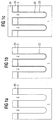
- a pad oxide layer 5 and one Padnitride layer 10 deposited, as shown in Figure 1a.
- another pad oxide layer (not shown) deposited and these layers are then removed by means of a also not shown photoresist mask and a corresponding Etching process structured into a so-called hard mask.
- this hard mask trenches 2 are formed a typical depth of about 1-10 ⁇ m in the silicon substrate 1 etched. Then the top pad oxide layer is removed, to get to the state shown in Fig. 1a.
- a cover oxide 5 ' is then placed on the resulting structure deposited.
- a special dielectric 70 with a high dielectric constant is then deposited on the resulting structure by means of the ALD or ALCVD method (atomic layer deposition).
- ALD atomic layer deposition
- ALCVD atomic layer chemical vapor deposition
- other suitable CVD methods can be used for the deposition.
- Suitable materials for the dielectric 60 with a high dielectric constant are in particular: Al 2 O 3 , Ta 2 O 5 , ZrO 2 , HfO 2 , Y 2 O 3 , La 2 O 3 , TiO 2 ; Al-Ta-O, Al-Zr-O, Al-Hf-O, Al-La-O, Al-Ti-O, Zr-YO, Zr-Si-O, Hf-Si-O, Si-ON, Ta-ON and similar materials.
- This deposition can be carried out with very good uniformity and conformity due to the ALD, ALCVD or CVD process.
- a collar oxide 5 ′′ is formed in the upper region of the trenches 2. This is done by a full-surface oxide deposition and a subsequent anisotropic etching of the oxide so that the Collar oxide 5 '' on the side walls in the upper trench area stop.
- the collar was made after Deposition of the dielectric 70 with a high dielectric constant educated.
- the collar is formed before deposition of the dielectric 70 with a high dielectric constant.
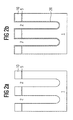
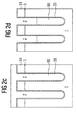
- the ASG layer 20 with a filling of the resulting structure undoped polycrystalline silicon 90 which is then used for Reaching the state shown in Figure 2d in the upper area the trench by isotropic dry chemical etching Will get removed.
- arsenic is made from the ASG 20 in the surrounding area of the silicon substrate 1 diffused out to form the buried plate 60.
- the deposition takes place in the next process step according to FIG. 2j of dielectric 70 with high dielectric constants by means of in connection with the first embodiment ALD or ALCVD method or CVD method already mentioned.
- the particularly suitable materials with high Dielectric constant have also already been related mentioned with the first embodiment.
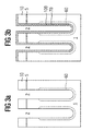
- the special dielectric 70 is then included high dielectric constant using the ALD or ALCVD method deposited on the resulting structure, like explained in detail in connection with Figure 1h.
- this is followed by the deposition of a metal electrode film 100 by means of the ALD or ALCVD method or another suitable CVD process.
- metal electrode 100 come as materials for the metal electrode 100 considered: TiN, WN, TaN, HfN, ZrN, Ti, W, Ta, Si, TaSiN, WSiN, TiAlN, WSi, MoSi, CoSi and in general metal-silicon nitrides or similar materials.
- arsenic-doped according to FIG. 3c polycrystalline silicon 80 on the resulting Structure deposited, so that the trenches 2 completely fills.
- poly silicon germanium could also be used be used for replenishment.
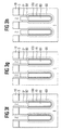
- a collar oxide 5 ′′ is formed in the upper region of the trenches 2. This is done by a full-surface oxide deposition and a subsequent anisotropic etching of the oxide so that the Collar oxide 5 '' on the side walls in the upper trench area stop.
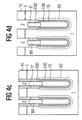
- a further metal electrode film is then made 100 'deposited analogously to the metal electrode film 100 and etched back anisotropically so that it is in the upper region of the trenches 2 stops.
- anisotropic etching can be used also be waived or the upper ditch area also completely filled with metal (i.e. without polysilicon 80 ') become.
- Arsenic-doped polysilicon is deposited 80 'and a corresponding etching back to the in Figure 4c shown state to achieve.
- the metal electrode film 100 'and the collar oxide 5' 'in the upper area of the trenches 2 expediently etched back by wet chemistry.
- 5a-e show the essentials for understanding the invention Method steps for producing a fifth exemplary embodiment of the trench capacitor according to the invention.
- FIG. 5a corresponds to that in FIG 2j shown state, its history in detail above explained in connection with the second embodiment has been.
- the metal electrode film subsequently follows 100 by means of the ALD or ALCVD process or the CVD process deposited on the resulting structure, and although in an analogous manner as discussed in connection with Figure 3b.
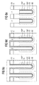
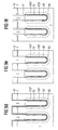
- 6a-h show the essentials for understanding the invention Method steps for producing a sixth exemplary embodiment of the trench capacitor according to the invention.
- a metal-insulator-metal structure is then deposited, consisting of the metal electrode layer 100 ′′, the dielectric layer 70 and the metal electrode layer 100 '' '.
- the deposition process and the materials used for these layers correspond to those the first and third embodiments explained above, and a repeated description of them is therefore made omit here.
- arsenic-doped according to FIG. 6c polycrystalline silicon 80 on the resulting Structure deposited, so that the trenches 2 completely fills.
- poly-silicon germanium could also be used be used for replenishment.
- a collar oxide 5 ′′ is formed in the upper region of the trenches 2. This is done by a full-surface oxide deposition and a subsequent anisotropic etching of the oxide so that the Collar oxide 5 '' on the side walls in the upper trench area stop.
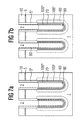
- the state shown in FIG. 7a corresponds to that in FIG 6f shown state, with another recess on the Polysilicon 80 was made so that the metal electrode layer 100 '' 'is partially exposed in trench 2.
- the further metal electrode layer 100 ' is deposited and anisotropically etched so that the metal electrode layer 100 'the Lining inner walls in the upper region of the trench 2.
- alternative anisotropic etching back can also be dispensed with or the upper trench area entirely with metal (i.e. without polysilicon 80 ').
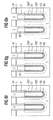
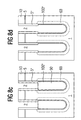
- FIG. 8a corresponds to that in FIG. 1g shown structure, wherein on the structure of Figure 1g Metal electrode film 100 '' according to the ALD or CVD process, was deposited as explained above. Furthermore was undoped polysilicon 90 over the structure thus obtained deposited and etched back to the top of Buried Plate 60.
- the metal electrode film is then etched back 100 '' in the exposed area by a corresponding isotropic etching process.
- the collar oxide 5 ′′ is then deposited and etched back anisotropically, as already described above. It this is followed by removal of the undoped polysilicon 90 in the lower one Trench area, resulting in the structure shown in Figure 8d leads.
- This eighth embodiment allows the collar self-aligned to the lower metal electrode 100 '' is.
- the metal electrode layer is deposited 100 ′′ on the structure shown in FIG Photoresist 30 was applied and etched back.
- the metal electrode layer is then etched back 100 ′′ and removal of the photoresist 30 by a corresponding etching process.
- the metal electrode layer 100 '' 'and the dielectric layer 70 also etched back to the structure shown in Figure 9e to obtain.
- a collar oxide 5 ′′ is formed in the upper region of the trenches 2. This is done by a full-surface oxide deposition and a subsequent anisotropic etching of the oxide so that the Collar oxide 5 '' on the side walls in the upper trench area stop.
- the collar is self-aligned to the dielectric 70 and applied to the upper electrode 100 '' '.
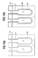
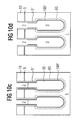
- FIG. 10a corresponds to the state according to Figure 2i, the history of which has already been described in detail explained with the above second embodiment has been.
- the metal electrode layer 100 '' deposited.
- the structure is then filled with photoresist 30 and Etch back photoresist 30 to that shown in Figure 10c Structure. Then the is etched back Metal electrode layer 100 '' in the exposed area and after removing the photoresist 30. This is shown in FIG. 10d shown.
- Arsenic-doped is deposited and etched back Polysilicon 80 or polysilicon germanium. This leads to the structure shown in Figure 10f.
- the materials listed are only examples and other materials with suitable properties replaceable.
Landscapes
- Engineering & Computer Science (AREA)
- Manufacturing & Machinery (AREA)
- Semiconductor Memories (AREA)
- Semiconductor Integrated Circuits (AREA)
Abstract
Description
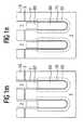
- Fig. 1a-n
- die zum Verständnis der Erfindung wesentlichen Verfahrensschritte zur Herstellung eines ersten Ausführungsbeispiels des erfindungsgemäßen Grabenkondensators;
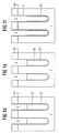
- Fig. 2a-m
- die zum Verständnis der Erfindung wesentlichen Verfahrensschritte zur Herstellung eines zweiten Ausführungsbeispiels des erfindungsgemäßen Grabenkondensators;
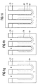
- Fig. 3a-h
- die zum Verständnis der Erfindung wesentlichen Verfahrensschritte zur Herstellung eines dritten Ausführungsbeispiels des erfindungsgemäßen Grabenkondensators;
- Fig. 4a-d
- die zum Verständnis der Erfindung wesentlichen Verfahrensschritte zur Herstellung eines vierten Ausführungsbeispiels des erfindungsgemäßen Grabenkondensators;
- Fig. 5a-e
- die zum Verständnis der Erfindung wesentlichen Verfahrensschritte zur Herstellung eines fünften Ausführungsbeispiels des erfindungsgemäßen Grabenkondensators;
- Fig. 6a-h
- die zum Verständnis der Erfindung wesentlichen Verfahrensschritte zur Herstellung eines sechsten Ausführungsbeispiels des erfindungsgemäßen Grabenkondensators;
- Fig. 7a-d
- die zum Verständnis der Erfindung wesentlichen Verfahrensschritte zur Herstellung eines siebenten Ausführungsbeispiels des erfindungsgemäßen Grabenkondensators;
- Fig. 8a-g
- die zum Verständnis der Erfindung wesentlichen Verfahrensschritte zur Herstellung eines achten Ausführungsbeispiels des erfindungsgemäßen Grabenkondensators;
- Fig. 9a-h
- die zum Verständnis der Erfindung wesentlichen Verfahrensschritte zur Herstellung eines neunten Ausführungsbeispiels des erfindungsgemäßen Grabenkondensators; und
- Fig. 10a-g
- die zum Verständnis der Erfindung wesentlichen Verfahrensschritte zur Herstellung eines zehnten Ausführungsbeispiels des erfindungsgemäßen Grabenkondensators.
- 1
- Siliziumsubstrat
- 3
- aufgeweiteter Bereich
- 5
- Padoxid
- 5'
- Deckoxid
- 5''
- Kragenoxid
- 10
- Padnitrid
- 20
- ASG
- 30
- Photolack
- 60
- Buried Plate
- 70
- Dielektrikum
- 80, 80'
- dotiertes Polysilizium
- 90
- undotiertes Polysilizium
- 100, 100', 100'', 100'''
- Metallelektrodenschicht
Claims (21)
- Grabenkondensator, insbesondere zur Verwendung in einer Halbleiter-Speicherzelle, mit:dadurch gekennzeichnet, daß die dielektrische Schicht (70) durch ein ALD- bzw. ALCVD-Verfahren oder ein CVD-Verfahren aufgebracht worden ist.einem Graben (2), der in einem Halbleitersubstrat (1) gebildet ist;einer im Graben (2) befindlichen ersten und zweiten leitenden Kondensatorplatte (60, 80; 60, 100; 100'', 100''');einer zwischen der ersten und zweiten Kondensatorplatte (60, 80; 60, 100; 100'', 100''') befindlichen dielektrischen Schicht (70) als Kondensatordielektrikum;einem Isolationskragen (5'') im oberen Bereich des Grabens (2); undeinem optionellen in den Graben (2) gefüllten leitenden Füllmaterial (80, 80');
- Grabenkondensator nach Anspruch 1,
dadurch gekennzeichnet, daß die erste Kondensatorplatte (60) ein Bereich erhöhter Dotierung (60) im Halbleitersubstrat (1) im unteren Bereich des Grabens (2) ist und die zweite Kondensatorplatte das leitende Füllmaterial (80, 80') ist. - Grabenkondensator, insbesondere zur Verwendung in einer Halbleiter-Speicherzelle, mit:wobei die erste Kondensatorplatte (60) ein Bereich erhöhter Dotierung (60) im Halbleitersubstrat (1) im unteren Bereich des Grabens (2) ist;einem Graben (2), der in einem Halbleitersubstrat (1) gebildet ist;einer im Graben (2) befindlichen ersten und zweiten leitenden Kondensatorplatte (60, 80; 60, 100; 100'', 100''');einer zwischen der ersten und zweiten Kondensatorplatte (60, 80; 60, 100; 100'', 100''') befindlichen dielektrischen Schicht (70) als Kondensatordielektrikum;einem Isolationskragen (5'') im oberen Bereich des Grabens(2); undeinem optionellen in den Graben (2) gefüllten leitenden Füllmaterial (80, 80');
dadurch gekennzeichnet, daß auf der dielektrischen Schicht (70) im Grabeninnern eine erste Metallelektrodenschicht (100) als zweite Kondensatorplatte vorgesehen ist. - Grabenkondensator nach Anspruch 3,
dadurch gekennzeichnet, daß im oberen Bereich des Grabens (2) eine zweite Metallelektrodenschicht (100') vorgesehen ist, welche mit der ersten Metallelektrodenschicht (100) in elektrischer Verbindung steht, wobei die zweite Metallelektrodenschicht (100') optionellerweise den oberen Grabenbereich ausfüllt. - Grabenkondensator, insbesondere zur Verwendung in einer Halbleiter-Speicherzelle, mit:dadurch gekennzeichnet, daß zwischen der dielektrischen Schicht (70) und dem Halbleitersubstrat (1) eine dritte Metallelektrodenschicht (100'') als erste Kondensatorplatte und andererseits der dielektrischen Schicht (70) eine vierte Metallelektrodenschicht (100''') als zweite Kondensatorplatte vorgesehen ist.einem Graben (2), der in einem Halbleitersubstrat (1) gebildet ist;einer im Graben (2) befindlichen ersten und zweiten leitenden Kondensatorplatte (60, 80; 60, 100; 100'', 100''');einer zwischen der ersten und zweiten Kondensatorplatte (60, 80; 60, 100; 100'', 100''') befindlichen dielektrischen Schicht (70) als Kondensatordielektrikum;einem Isolationskragen (5'') im oberen Bereich des Grabens (2); undeinem optionellen in den Graben (2) gefüllten leitenden Füllmaterial (80');
- Grabenkondensator nach Anspruch 5,
dadurch gekennzeichnet, daß im oberen Bereich des Grabens (2) eine zweite Metallelektrodenschicht (100') vorgesehen ist, welche mit der vierten Metallelektrodenschicht (100''') in elektrischer Verbindung steht, wobei die zweite Metallelektrodenschicht (100') optionellerweise den oberen Grabenbereich ausfüllt. - Grabenkondensator nach Anspruch 5 oder 6,
dadurch gekennzeichnet, daß die dielektrische Schicht (70) und die vierte Metallelektrodenschicht (100''') in den Bereich des Isolationskragens (5'') geführt sind. - Grabenkondensator nach Anspruch 7,
dadurch gekennzeichnet, daß die dritte Metallelektrodenschicht (100''') in den Bereich des Isolationskragens (5'') geführt ist. - Grabenkondensator nach einem der Ansprüche 3 bis 8,
dadurch gekennzeichnet, daß die erste oder zweite oder dritte oder vierte Metallelektrodenschicht (100, 100', 100'', 100'') oder die dielektrische Schicht (70) durch ein ALD- bzw. ALCVD-Verfahren oder ein CVD-Verfahren aufgebracht worden ist. - Grabenkondensator nach einem der Ansprüche 3 bis 9,
dadurch gekennzeichnet, daß die erste oder zweite oder dritte oder vierte Metallelektrodenschicht (100, 100', 100'', 100''') mindestens eines der folgenden Materialien aufweist:TiN, WN, TaN, HfN, ZrN, Ti, W, Ta, Si, TaSiN, WSiN, TiAlN, WSi, MoSi, CoSi. - Grabenkondensator nach einem der vorhergehenden Ansprüche,
dadurch gekennzeichnet, daß der Graben (2) einen unteren aufgeweiteten Bereich (3) aufweist. - Grabenkondensator nach einem der vorhergehenden Ansprüche,
dadurch gekennzeichnet, daß die dielektrische Schicht (70) mindestens eines der folgenden Materialien aufweist:Al2O3, Ta2O5, ZrO2, HfO2, Y2O3, La2O3, TiO2; Al-Ta-O, Al-Zr-O, Al-Hf-O, Al-La-O, Al-Ti-O, Zr-Y-O, Zr-Si-O, Hf-Si-O, Si-O-N, Ta-O-N, Gd2O3, SnO3, La-Si-O, Ti-Si-O, LaAlO3, ZrTiO4, (Zr, Sn)TiO4, SrZrO4, LaAlO4, BaZrO3. - Grabenkondensator nach einem der vorhergehenden Ansprüche,
dadurch gekennzeichnet, daß das leitende Füllmaterial (80, 80') aus einer ersten leitenden Füllschicht (80) im unteren Grabenbereich und einer zweiten leitenden Füllschicht (80') im oberen Grabenbereich zusammengesetzt ist. - Verfahren zur Herstellung eine Grabenkondensators, insbesondere zur Verwendung in einer Halbleiter-Speicherzelle, mit den Schritten:dadurch gekennzeichnet, daß die dielektrische Schicht (70) durch ein ALD- bzw. ALCVD-Verfahren oder ein CVD-Verfahren aufgebracht wird.Bilden eines Grabens (2) in einem Halbleitersubstrat (1);Vorsehen einer ersten und zweiten leitenden Kondensatorplatte (60, 80; 60, 100; 100'', 100''') im Graben (2);Vorsehen einer dielektrischen Schicht (70) als Kondensatordielektrikum zwischen der ersten und zweiten Kondensatorplatte (60, 80; 60, 100; 100'', 100''');Bilden eines Isolationskragens (5'') im oberen Bereich des Grabens (2); undoptionelles Auffüllen eines leitenden Füllmaterials (80, 80') in den Graben (2);
- Verfahren zur Herstellung eine Grabenkondensators, insbesondere zur Verwendung in einer Halbleiter-Speicherzelle, mit den Schritten:dadurch gekennzeichnet, daß auf der dielektrischen Schicht (70) im Grabeninnern eine erste Metallelektrodenschicht (100) als zweite Kondensatorplatte vorgesehen wird.Bilden eines Grabens (2) in einem Halbleitersubstrat (1);Vorsehen einer ersten und zweiten leitenden Kondensatorplatte (60, 80; 60, 100; 100'', 100''') im Graben (2);Vorsehen einer dielektrischen Schicht (70) als Kondensatordielektrikum zwischen der ersten und zweiten Kondensatorplatte (60, 80; 60, 100; 100'', 100''');Bilden eines Isolationskragens (5'') im oberen Bereich des Grabens (2); undoptionelles Auffüllen eines leitenden Füllmaterials (80, 80') in den Graben (2);
- Verfahren nach Anspruch 15,
dadurch gekennzeichnet, daß im oberen Bereich des Grabens (2) eine zweite Metallelektrodenschicht (100') vorgesehen wird, welche mit der ersten Metallelektrodenschicht (100) in elektrischer Verbindung steht. - Verfahren zur Herstellung eine Grabenkondensators, insbesondere zur Verwendung in einer Halbleiter-Speicherzelle, mit den Schritten:dadurch gekennzeichnet, daß zwischen der dielektrischen Schicht (70) und dem Halbleitersubstrat (1) eine dritte Metallelektrodenschicht (100'') als erste Kondensatorplatte und andererseits der dielektrischen Schicht (70) eine vierte Metallelektrodenschicht (100''') als zweite Kondensatorplatte vorgesehen wird.Bilden eines Grabens (2) in einem Halbleitersubstrat (1);Vorsehen einer ersten und zweiten leitenden Kondensatorplatte (60, 80; 60, 100; 100'', 100''') im Graben (2);Vorsehen einer dielektrischen Schicht (70) als Kondensatordielektrikum zwischen der ersten und zweiten Kondensatorplatte (60, 80; 60, 100; 100'', 100''');Bilden eines Isolationskragens (5'') im oberen Bereich des Grabens (2); undoptionelles Auffüllen eines leitenden Füllmaterials (80, 80') in den Graben (2);
- Verfahren nach Anspruch 17,
dadurch gekennzeichnet, daß zwischen dem Isolationskragen (5'') und dem leitenden Füllmaterial (80, 80') im oberen Bereich des Grabens (2) eine zweite Metallelektrodenschicht (100') vorgesehen wird, welche mit der vierten Metallelektrodenschicht (100''') in elektrischer Verbindung steht. - Verfahren nach Anspruch 17 oder 18,
dadurch gekennzeichnet, daß die dielektrische Schicht (70) und die vierte Metallelektrodenschicht (100''') in den Bereich des Isolationskragens (5'') geführt werden. - Verfahren nach Anspruch 19,
dadurch gekennzeichnet, daß die dritte Metallelektrodenschicht (100''') in den Bereich des Isolationskragens (5'') geführt wird. - Verfahren nach einem der Ansprüche 16 bis 20,
dadurch gekennzeichnet, daß die erste oder zweite oder dritte oder vierte Metallelektrodenschicht (100, 100', 100'', 100''') oder die dielektrische Schicht (70) durch ein ALD- bzw. ALCVD-Verfahren oder ein CVD-Verfahren aufgebracht wird.
Applications Claiming Priority (2)
| Application Number | Priority Date | Filing Date | Title |
|---|---|---|---|
| DE10034003 | 2000-07-07 | ||
| DE10034003A DE10034003A1 (de) | 2000-07-07 | 2000-07-07 | Grabenkondensator mit Isolationskragen und entsprechendes Herstellungsverfahren |
Publications (3)
| Publication Number | Publication Date |
|---|---|
| EP1170804A2 true EP1170804A2 (de) | 2002-01-09 |
| EP1170804A3 EP1170804A3 (de) | 2004-06-09 |
| EP1170804B1 EP1170804B1 (de) | 2008-04-02 |
Family
ID=7648752
Family Applications (1)
| Application Number | Title | Priority Date | Filing Date |
|---|---|---|---|
| EP01115516A Expired - Lifetime EP1170804B1 (de) | 2000-07-07 | 2001-06-27 | Grabenkondensator mit Isolationskragen und entsprechendes Herstellungsverfahren |
Country Status (4)
| Country | Link |
|---|---|
| US (1) | US20020014647A1 (de) |
| EP (1) | EP1170804B1 (de) |
| DE (2) | DE10034003A1 (de) |
| TW (1) | TWI225707B (de) |
Cited By (6)
| Publication number | Priority date | Publication date | Assignee | Title |
|---|---|---|---|---|
| US6720027B2 (en) | 2002-04-08 | 2004-04-13 | Applied Materials, Inc. | Cyclical deposition of a variable content titanium silicon nitride layer |
| US7067439B2 (en) | 2002-06-14 | 2006-06-27 | Applied Materials, Inc. | ALD metal oxide deposition process using direct oxidation |
| US7262133B2 (en) | 2003-01-07 | 2007-08-28 | Applied Materials, Inc. | Enhancement of copper line reliability using thin ALD tan film to cap the copper line |
| US7547952B2 (en) | 2003-04-04 | 2009-06-16 | Applied Materials, Inc. | Method for hafnium nitride deposition |
| US8119210B2 (en) | 2004-05-21 | 2012-02-21 | Applied Materials, Inc. | Formation of a silicon oxynitride layer on a high-k dielectric material |
| US8323754B2 (en) | 2004-05-21 | 2012-12-04 | Applied Materials, Inc. | Stabilization of high-k dielectric materials |
Families Citing this family (47)
| Publication number | Priority date | Publication date | Assignee | Title |
|---|---|---|---|---|
| US6620723B1 (en) | 2000-06-27 | 2003-09-16 | Applied Materials, Inc. | Formation of boride barrier layers using chemisorption techniques |
| DE10114956C2 (de) * | 2001-03-27 | 2003-06-18 | Infineon Technologies Ag | Verfahren zum Herstellen einer dielektrischen Schicht als Isolatorschicht für einen Grabenkondensator |
| US6753618B2 (en) * | 2002-03-11 | 2004-06-22 | Micron Technology, Inc. | MIM capacitor with metal nitride electrode materials and method of formation |
| DE10211544C1 (de) | 2002-03-15 | 2003-11-27 | Infineon Technologies Ag | Verfahren zur Herstellung einer Kondensatorelektrode eines Grabenkondensators aus flüssiger Phase |
| US6846516B2 (en) | 2002-04-08 | 2005-01-25 | Applied Materials, Inc. | Multiple precursor cyclical deposition system |
| US20030235961A1 (en) * | 2002-04-17 | 2003-12-25 | Applied Materials, Inc. | Cyclical sequential deposition of multicomponent films |
| US6897508B2 (en) | 2002-05-01 | 2005-05-24 | Sundew Technologies, Llc | Integrated capacitor with enhanced capacitance density and method of fabricating same |
| US20030232501A1 (en) * | 2002-06-14 | 2003-12-18 | Kher Shreyas S. | Surface pre-treatment for enhancement of nucleation of high dielectric constant materials |
| US6858547B2 (en) | 2002-06-14 | 2005-02-22 | Applied Materials, Inc. | System and method for forming a gate dielectric |
| US6921702B2 (en) * | 2002-07-30 | 2005-07-26 | Micron Technology Inc. | Atomic layer deposited nanolaminates of HfO2/ZrO2 films as gate dielectrics |
| DE10234735A1 (de) * | 2002-07-30 | 2004-02-12 | Infineon Technologies Ag | Verfahren zum vertikalen Strukturieren von Substraten in der Halbleiterprozesstechnik mittels inkonformer Abscheidung |
| DE10234734A1 (de) | 2002-07-30 | 2004-02-12 | Infineon Technologies Ag | Verwendung von Masken aus Metalloxiden zur Bearbeitung von Oberflächen bei der Herstellung von Mikrochips |
| DE10240106A1 (de) | 2002-08-30 | 2004-03-11 | Infineon Technologies Ag | Ausbildung einer elektrischen Verbindung zwischen Strkturen in einem Halbleitersubstrat |
| TW554521B (en) * | 2002-09-16 | 2003-09-21 | Nanya Technology Corp | Process for forming a bottle-shaped trench |
| US7101813B2 (en) * | 2002-12-04 | 2006-09-05 | Micron Technology Inc. | Atomic layer deposited Zr-Sn-Ti-O films |
| KR101159070B1 (ko) * | 2003-03-11 | 2012-06-25 | 삼성전자주식회사 | 고유전율 산화막 형성방법, 이 방법으로 형성된 유전막이구비된 커패시터 및 그 제조방법 |
| US6909137B2 (en) | 2003-04-07 | 2005-06-21 | International Business Machines Corporation | Method of creating deep trench capacitor using a P+ metal electrode |
| US6967137B2 (en) * | 2003-07-07 | 2005-11-22 | International Business Machines Corporation | Forming collar structures in deep trench capacitors with thermally stable filler material |
| JP3956225B2 (ja) * | 2003-08-26 | 2007-08-08 | 株式会社トリケミカル研究所 | 膜形成方法 |
| DE10344039B4 (de) * | 2003-09-23 | 2011-06-01 | Qimonda Ag | Elektrisch programmierbarer nichtflüchtiger Speicher auf Basis eines Schwellwert veränderbaren MOSFET und ein Verfahren zu dessen Herstellung |
| DE102004019090B4 (de) * | 2004-04-20 | 2006-05-04 | Infineon Technologies Ag | Grabenkondensator mit Isolationskragen |
| US20050252449A1 (en) | 2004-05-12 | 2005-11-17 | Nguyen Son T | Control of gas flow and delivery to suppress the formation of particles in an MOCVD/ALD system |
| US20060062917A1 (en) * | 2004-05-21 | 2006-03-23 | Shankar Muthukrishnan | Vapor deposition of hafnium silicate materials with tris(dimethylamino)silane |
| US20060019033A1 (en) * | 2004-05-21 | 2006-01-26 | Applied Materials, Inc. | Plasma treatment of hafnium-containing materials |
| US20060153995A1 (en) * | 2004-05-21 | 2006-07-13 | Applied Materials, Inc. | Method for fabricating a dielectric stack |
| US7588988B2 (en) * | 2004-08-31 | 2009-09-15 | Micron Technology, Inc. | Method of forming apparatus having oxide films formed using atomic layer deposition |
| KR100728962B1 (ko) * | 2004-11-08 | 2007-06-15 | 주식회사 하이닉스반도체 | 지르코늄산화막을 갖는 반도체소자의 캐패시터 및 그 제조방법 |
| DE102004059668B3 (de) * | 2004-12-10 | 2006-07-13 | Infineon Technologies Ag | Halbleitertechnologieverfahren zur Herstellung einer leitfähigen Schicht |
| KR20060072338A (ko) * | 2004-12-23 | 2006-06-28 | 주식회사 하이닉스반도체 | 유전체막 형성방법 및 이를 이용한 반도체 소자의캐패시터 형성방법 |
| US20070020890A1 (en) * | 2005-07-19 | 2007-01-25 | Applied Materials, Inc. | Method and apparatus for semiconductor processing |
| US7927948B2 (en) | 2005-07-20 | 2011-04-19 | Micron Technology, Inc. | Devices with nanocrystals and methods of formation |
| US20070049043A1 (en) * | 2005-08-23 | 2007-03-01 | Applied Materials, Inc. | Nitrogen profile engineering in HI-K nitridation for device performance enhancement and reliability improvement |
| US7402534B2 (en) | 2005-08-26 | 2008-07-22 | Applied Materials, Inc. | Pretreatment processes within a batch ALD reactor |
| KR100648860B1 (ko) * | 2005-09-08 | 2006-11-24 | 주식회사 하이닉스반도체 | 유전막 및 그 형성방법과, 상기 유전막을 구비한 반도체메모리 소자 및 그 제조방법 |
| US20070065578A1 (en) * | 2005-09-21 | 2007-03-22 | Applied Materials, Inc. | Treatment processes for a batch ALD reactor |
| KR100670747B1 (ko) | 2005-11-28 | 2007-01-17 | 주식회사 하이닉스반도체 | 반도체소자의 캐패시터 제조 방법 |
| US7294554B2 (en) * | 2006-02-10 | 2007-11-13 | International Business Machines Corporation | Method to eliminate arsenic contamination in trench capacitors |
| US7964514B2 (en) * | 2006-03-02 | 2011-06-21 | Applied Materials, Inc. | Multiple nitrogen plasma treatments for thin SiON dielectrics |
| US20070252299A1 (en) * | 2006-04-27 | 2007-11-01 | Applied Materials, Inc. | Synchronization of precursor pulsing and wafer rotation |
| US7798096B2 (en) | 2006-05-05 | 2010-09-21 | Applied Materials, Inc. | Plasma, UV and ion/neutral assisted ALD or CVD in a batch tool |
| US7846791B2 (en) * | 2007-11-08 | 2010-12-07 | International Business Machines Corporation | Structure for a trench capacitor |
| US7659158B2 (en) | 2008-03-31 | 2010-02-09 | Applied Materials, Inc. | Atomic layer deposition processes for non-volatile memory devices |
| US20100062149A1 (en) | 2008-09-08 | 2010-03-11 | Applied Materials, Inc. | Method for tuning a deposition rate during an atomic layer deposition process |
| US8491967B2 (en) | 2008-09-08 | 2013-07-23 | Applied Materials, Inc. | In-situ chamber treatment and deposition process |
| US20110298089A1 (en) * | 2010-06-03 | 2011-12-08 | International Business Machines Corporation | Trench capacitor and method of fabrication |
| US8502293B2 (en) * | 2010-12-22 | 2013-08-06 | Intel Corporation | Capacitor with recessed plate portion for dynamic random access memory (DRAM) and method to form the same |
| US20130075801A1 (en) * | 2011-09-23 | 2013-03-28 | Infineon Technologies Austria Ag | Self-adjusted capacitive structure |
Family Cites Families (11)
| Publication number | Priority date | Publication date | Assignee | Title |
|---|---|---|---|---|
| FR2575335B1 (fr) * | 1984-12-21 | 1987-06-19 | Thomson Csf | Element capacitif integre sur une pastille de circuit integre, et procede de realisation de cet element capacitif |
| JPH04328861A (ja) * | 1991-04-26 | 1992-11-17 | Texas Instr Japan Ltd | 半導体集積回路装置及びその製造方法 |
| RU2082258C1 (ru) * | 1991-08-14 | 1997-06-20 | Сименс АГ | Схемная структура с по меньшей мере одним конденсатором и способ ее изготовления |
| JPH0637275A (ja) * | 1992-07-13 | 1994-02-10 | Toshiba Corp | 半導体記憶装置及びその製造方法 |
| US5998821A (en) * | 1997-05-21 | 1999-12-07 | Kabushiki Kaisha Toshiba | Dynamic ram structure having a trench capacitor |
| US5945704A (en) * | 1998-04-06 | 1999-08-31 | Siemens Aktiengesellschaft | Trench capacitor with epi buried layer |
| US6018174A (en) * | 1998-04-06 | 2000-01-25 | Siemens Aktiengesellschaft | Bottle-shaped trench capacitor with epi buried layer |
| US6310375B1 (en) * | 1998-04-06 | 2001-10-30 | Siemens Aktiengesellschaft | Trench capacitor with isolation collar and corresponding manufacturing method |
| KR20000013654A (ko) * | 1998-08-12 | 2000-03-06 | 윤종용 | 원자층 증착 방법으로 형성한 알루미나/알루미늄나이트라이드복합 유전체막을 갖는 캐패시터와 그제조 방법 |
| US6034390A (en) * | 1999-06-25 | 2000-03-07 | Infineon Technologies North America Corp. | Multi-bit trench capacitor |
| TW426947B (en) * | 1999-12-09 | 2001-03-21 | Mosel Vitelic Inc | Method of producing trench capacitor |
-
2000
- 2000-07-07 DE DE10034003A patent/DE10034003A1/de not_active Ceased
-
2001
- 2001-06-27 EP EP01115516A patent/EP1170804B1/de not_active Expired - Lifetime
- 2001-06-27 DE DE50113806T patent/DE50113806D1/de not_active Expired - Fee Related
- 2001-06-28 TW TW090115833A patent/TWI225707B/zh not_active IP Right Cessation
- 2001-07-06 US US09/899,189 patent/US20020014647A1/en not_active Abandoned
Cited By (6)
| Publication number | Priority date | Publication date | Assignee | Title |
|---|---|---|---|---|
| US6720027B2 (en) | 2002-04-08 | 2004-04-13 | Applied Materials, Inc. | Cyclical deposition of a variable content titanium silicon nitride layer |
| US7067439B2 (en) | 2002-06-14 | 2006-06-27 | Applied Materials, Inc. | ALD metal oxide deposition process using direct oxidation |
| US7262133B2 (en) | 2003-01-07 | 2007-08-28 | Applied Materials, Inc. | Enhancement of copper line reliability using thin ALD tan film to cap the copper line |
| US7547952B2 (en) | 2003-04-04 | 2009-06-16 | Applied Materials, Inc. | Method for hafnium nitride deposition |
| US8119210B2 (en) | 2004-05-21 | 2012-02-21 | Applied Materials, Inc. | Formation of a silicon oxynitride layer on a high-k dielectric material |
| US8323754B2 (en) | 2004-05-21 | 2012-12-04 | Applied Materials, Inc. | Stabilization of high-k dielectric materials |
Also Published As
| Publication number | Publication date |
|---|---|
| DE50113806D1 (de) | 2008-05-15 |
| EP1170804A3 (de) | 2004-06-09 |
| TWI225707B (en) | 2004-12-21 |
| US20020014647A1 (en) | 2002-02-07 |
| DE10034003A1 (de) | 2002-01-24 |
| EP1170804B1 (de) | 2008-04-02 |
Similar Documents
| Publication | Publication Date | Title |
|---|---|---|
| EP1170804B1 (de) | Grabenkondensator mit Isolationskragen und entsprechendes Herstellungsverfahren | |
| DE10142580B4 (de) | Verfahren zur Herstellung einer Grabenstrukturkondensatoreinrichtung | |
| DE19930748C2 (de) | Verfahren zur Herstellung von EEPROM- und DRAM-Grabenspeicherzellbereichen auf einem Chip | |
| DE19521489B4 (de) | Kondensatorplatte und Kondensator, je in einer Halbleitervorrichtung gebildet, die Verwendung eines solchen Kondensators als Speicherkondensator einer Halbleitervorrichtung, Verfahren zur Herstellung eines Kondensators und Verwendung eines solchen Verfahrens zur Herstellung von DRAM-Vorrichtungen | |
| DE102018122648A1 (de) | Speichervorrichtungen und Verfahren zum Herstellen derselben | |
| DE19944012B4 (de) | Grabenkondensator mit Kondensatorelektroden und entsprechendes Herstellungsverfahren | |
| DE19941148B4 (de) | Speicher mit Grabenkondensator und Auswahltransistor und Verfahren zu seiner Herstellung | |
| DE69910293T2 (de) | Verfahren mit verbesserter Kontrollierbarkeit einer vergrabenen Schicht | |
| EP0887863A2 (de) | DRAM mit selbstverstärkenden Speicherzellen | |
| EP0766312A1 (de) | Selbstverstärkende DRAM-Speicherzellenanordnung | |
| DE19946719A1 (de) | Grabenkondensator und Verfahren zu seiner Herstellung | |
| EP1145319B1 (de) | Integrierte schaltungsanordnung und verfahren zu deren herstellung | |
| DE10045694A1 (de) | Halbleiterspeicherzelle mit Grabenkondensator und Auswahltransistor und Verfahren zu ihrer Herstellung | |
| DE19843641A1 (de) | Grabenkondensator mit Isolationskragen und entsprechendes Herstellungsverfahren | |
| EP0973201A1 (de) | Stapelkondensator und entsprechendes Herstellungsverfahren | |
| DE10128193C1 (de) | Ein-Transistor-Speicherzellenanordnung und Verfahren zu deren Herstellung | |
| DE10328634B3 (de) | Verfahren zur Herstellung eines Buried-Strap-Kontakts für einen Speicherkondensator | |
| DE10111760A1 (de) | Verfahren zur Herstellung einer Speicherzelle eines Halbleiterspeichers | |
| DE10128211C1 (de) | Speicher mit einer Speicherzelle, umfassend einen Auswahltransistor und einen Speicherkondensator sowie Verfahren zu seiner Herstellung | |
| DE10226583A1 (de) | DRAM-Speicherzelle für schnellen Schreib-/Lesezugriff | |
| DE102004005694B3 (de) | Grabenkondensator mit Isolationskragen und entsprechendes Herstellungsverfahren | |
| WO2003003462A2 (de) | Grabenkondensator und entsprechendes herstellungsverfahren | |
| DE19923262C1 (de) | Verfahren zur Erzeugung einer Speicherzellenanordnung | |
| EP1296369A1 (de) | Verfahren zur Herstellung von Gateoxyd für Trench Gate DRAM Zellen | |
| DE102005057255B4 (de) | Speicherkondensator und Verfahren zum Herstellen eines solchen Speicherkondensators |
Legal Events
| Date | Code | Title | Description |
|---|---|---|---|
| PUAI | Public reference made under article 153(3) epc to a published international application that has entered the european phase |
Free format text: ORIGINAL CODE: 0009012 |
|
| AK | Designated contracting states |
Kind code of ref document: A2 Designated state(s): AT BE CH CY DE DK ES FI FR GB GR IE IT LI LU MC NL PT SE TR |
|
| AX | Request for extension of the european patent |
Free format text: AL;LT;LV;MK;RO;SI |
|
| PUAL | Search report despatched |
Free format text: ORIGINAL CODE: 0009013 |
|
| AK | Designated contracting states |
Kind code of ref document: A3 Designated state(s): AT BE CH CY DE DK ES FI FR GB GR IE IT LI LU MC NL PT SE TR |
|
| AX | Request for extension of the european patent |
Extension state: AL LT LV MK RO SI |
|
| AKX | Designation fees paid | ||
| 17P | Request for examination filed |
Effective date: 20041005 |
|
| RBV | Designated contracting states (corrected) |
Designated state(s): DE GB IE |
|
| REG | Reference to a national code |
Ref country code: DE Ref legal event code: 8566 |
|
| 17Q | First examination report despatched |
Effective date: 20071022 |
|
| GRAP | Despatch of communication of intention to grant a patent |
Free format text: ORIGINAL CODE: EPIDOSNIGR1 |
|
| GRAS | Grant fee paid |
Free format text: ORIGINAL CODE: EPIDOSNIGR3 |
|
| GRAA | (expected) grant |
Free format text: ORIGINAL CODE: 0009210 |
|
| AK | Designated contracting states |
Kind code of ref document: B1 Designated state(s): DE GB IE |
|
| REG | Reference to a national code |
Ref country code: GB Ref legal event code: FG4D Free format text: NOT ENGLISH |
|
| REG | Reference to a national code |
Ref country code: IE Ref legal event code: FG4D Free format text: LANGUAGE OF EP DOCUMENT: GERMAN |
|
| REF | Corresponds to: |
Ref document number: 50113806 Country of ref document: DE Date of ref document: 20080515 Kind code of ref document: P |
|
| REG | Reference to a national code |
Ref country code: IE Ref legal event code: FD4D |
|
| PGFP | Annual fee paid to national office [announced via postgrant information from national office to epo] |
Ref country code: DE Payment date: 20080812 Year of fee payment: 8 |
|
| PG25 | Lapsed in a contracting state [announced via postgrant information from national office to epo] |
Ref country code: IE Free format text: LAPSE BECAUSE OF FAILURE TO SUBMIT A TRANSLATION OF THE DESCRIPTION OR TO PAY THE FEE WITHIN THE PRESCRIBED TIME-LIMIT Effective date: 20080402 |
|
| PLBE | No opposition filed within time limit |
Free format text: ORIGINAL CODE: 0009261 |
|
| STAA | Information on the status of an ep patent application or granted ep patent |
Free format text: STATUS: NO OPPOSITION FILED WITHIN TIME LIMIT |
|
| 26N | No opposition filed |
Effective date: 20090106 |
|
| GBPC | Gb: european patent ceased through non-payment of renewal fee |
Effective date: 20080702 |
|
| PG25 | Lapsed in a contracting state [announced via postgrant information from national office to epo] |
Ref country code: GB Free format text: LAPSE BECAUSE OF NON-PAYMENT OF DUE FEES Effective date: 20080702 |
|
| PG25 | Lapsed in a contracting state [announced via postgrant information from national office to epo] |
Ref country code: DE Free format text: LAPSE BECAUSE OF NON-PAYMENT OF DUE FEES Effective date: 20100101 |