EP1156580A2 - Appareil d'alimentation de puisance à découpage - Google Patents
Appareil d'alimentation de puisance à découpage Download PDFInfo
- Publication number
- EP1156580A2 EP1156580A2 EP01304310A EP01304310A EP1156580A2 EP 1156580 A2 EP1156580 A2 EP 1156580A2 EP 01304310 A EP01304310 A EP 01304310A EP 01304310 A EP01304310 A EP 01304310A EP 1156580 A2 EP1156580 A2 EP 1156580A2
- Authority
- EP
- European Patent Office
- Prior art keywords
- switching
- switching device
- voltage
- circuit
- primary
- Prior art date
- Legal status (The legal status is an assumption and is not a legal conclusion. Google has not performed a legal analysis and makes no representation as to the accuracy of the status listed.)
- Withdrawn
Links
Images


Classifications
-
- H—ELECTRICITY
- H02—GENERATION; CONVERSION OR DISTRIBUTION OF ELECTRIC POWER
- H02M—APPARATUS FOR CONVERSION BETWEEN AC AND AC, BETWEEN AC AND DC, OR BETWEEN DC AND DC, AND FOR USE WITH MAINS OR SIMILAR POWER SUPPLY SYSTEMS; CONVERSION OF DC OR AC INPUT POWER INTO SURGE OUTPUT POWER; CONTROL OR REGULATION THEREOF
- H02M3/00—Conversion of dc power input into dc power output
- H02M3/22—Conversion of dc power input into dc power output with intermediate conversion into ac
- H02M3/24—Conversion of dc power input into dc power output with intermediate conversion into ac by static converters
- H02M3/28—Conversion of dc power input into dc power output with intermediate conversion into ac by static converters using discharge tubes with control electrode or semiconductor devices with control electrode to produce the intermediate ac
- H02M3/325—Conversion of dc power input into dc power output with intermediate conversion into ac by static converters using discharge tubes with control electrode or semiconductor devices with control electrode to produce the intermediate ac using devices of a triode or a transistor type requiring continuous application of a control signal
- H02M3/335—Conversion of dc power input into dc power output with intermediate conversion into ac by static converters using discharge tubes with control electrode or semiconductor devices with control electrode to produce the intermediate ac using devices of a triode or a transistor type requiring continuous application of a control signal using semiconductor devices only
- H02M3/338—Conversion of dc power input into dc power output with intermediate conversion into ac by static converters using discharge tubes with control electrode or semiconductor devices with control electrode to produce the intermediate ac using devices of a triode or a transistor type requiring continuous application of a control signal using semiconductor devices only in a self-oscillating arrangement
- H02M3/3385—Conversion of dc power input into dc power output with intermediate conversion into ac by static converters using discharge tubes with control electrode or semiconductor devices with control electrode to produce the intermediate ac using devices of a triode or a transistor type requiring continuous application of a control signal using semiconductor devices only in a self-oscillating arrangement with automatic control of output voltage or current
-
- H—ELECTRICITY
- H02—GENERATION; CONVERSION OR DISTRIBUTION OF ELECTRIC POWER
- H02M—APPARATUS FOR CONVERSION BETWEEN AC AND AC, BETWEEN AC AND DC, OR BETWEEN DC AND DC, AND FOR USE WITH MAINS OR SIMILAR POWER SUPPLY SYSTEMS; CONVERSION OF DC OR AC INPUT POWER INTO SURGE OUTPUT POWER; CONTROL OR REGULATION THEREOF
- H02M3/00—Conversion of dc power input into dc power output
- H02M3/01—Resonant DC/DC converters
-
- H—ELECTRICITY
- H02—GENERATION; CONVERSION OR DISTRIBUTION OF ELECTRIC POWER
- H02M—APPARATUS FOR CONVERSION BETWEEN AC AND AC, BETWEEN AC AND DC, OR BETWEEN DC AND DC, AND FOR USE WITH MAINS OR SIMILAR POWER SUPPLY SYSTEMS; CONVERSION OF DC OR AC INPUT POWER INTO SURGE OUTPUT POWER; CONTROL OR REGULATION THEREOF
- H02M3/00—Conversion of dc power input into dc power output
- H02M3/22—Conversion of dc power input into dc power output with intermediate conversion into ac
- H02M3/24—Conversion of dc power input into dc power output with intermediate conversion into ac by static converters
- H02M3/28—Conversion of dc power input into dc power output with intermediate conversion into ac by static converters using discharge tubes with control electrode or semiconductor devices with control electrode to produce the intermediate ac
- H02M3/325—Conversion of dc power input into dc power output with intermediate conversion into ac by static converters using discharge tubes with control electrode or semiconductor devices with control electrode to produce the intermediate ac using devices of a triode or a transistor type requiring continuous application of a control signal
- H02M3/335—Conversion of dc power input into dc power output with intermediate conversion into ac by static converters using discharge tubes with control electrode or semiconductor devices with control electrode to produce the intermediate ac using devices of a triode or a transistor type requiring continuous application of a control signal using semiconductor devices only
- H02M3/33569—Conversion of dc power input into dc power output with intermediate conversion into ac by static converters using discharge tubes with control electrode or semiconductor devices with control electrode to produce the intermediate ac using devices of a triode or a transistor type requiring continuous application of a control signal using semiconductor devices only having several active switching elements
- H02M3/33571—Half-bridge at primary side of an isolation transformer
-
- Y—GENERAL TAGGING OF NEW TECHNOLOGICAL DEVELOPMENTS; GENERAL TAGGING OF CROSS-SECTIONAL TECHNOLOGIES SPANNING OVER SEVERAL SECTIONS OF THE IPC; TECHNICAL SUBJECTS COVERED BY FORMER USPC CROSS-REFERENCE ART COLLECTIONS [XRACs] AND DIGESTS
- Y02—TECHNOLOGIES OR APPLICATIONS FOR MITIGATION OR ADAPTATION AGAINST CLIMATE CHANGE
- Y02B—CLIMATE CHANGE MITIGATION TECHNOLOGIES RELATED TO BUILDINGS, e.g. HOUSING, HOUSE APPLIANCES OR RELATED END-USER APPLICATIONS
- Y02B70/00—Technologies for an efficient end-user side electric power management and consumption
- Y02B70/10—Technologies improving the efficiency by using switched-mode power supplies [SMPS], i.e. efficient power electronics conversion e.g. power factor correction or reduction of losses in power supplies or efficient standby modes
Definitions
- the present invention relates to a switching power supply circuit to be provided as a power supply for various electronic apparatus.
- Switching power supply circuits employing switching converters such as flyback converters and forward converters are widely known. These switching converters form a rectangular waveform in switching operation, and therefore there is a limit to suppression of switching noise. It is also known that because of their operating characteristics, there is a limit to improvement of power conversion efficiency.
- Figs. 9 and 10 are circuit diagrams each showing an example of a prior art switching power supply circuit employing a resonance type converter.
- This voltage resonance type converter is externally excited, and a MOS-FET, for example, is used as a switching device Q1.
- a capacitor Cr is connected in parallel with a drain and a source of the switching device Q1. Capacitance of the capacitor Cr and leakage inductance obtained at a primary winding N1 of an isolating converter transformer PIT form a voltage resonant circuit.
- the parallel resonant circuit performs resonant operation according to switching operation of the switching device Q1.
- a clamp diode (so-called body diode) DD is connected in parallel with the drain and source of the switching device Q1.
- the clamp diode DD forms a path of clamp current that flows during an off period of the switching device.
- the drain of the switching device Q1 is connected to an oscillating circuit 11 in a switching driver 10.
- An output of the drain supplied to the oscillating circuit 11 is used to variably control an on period of switching operation of the switching device Q1 in switching frequency control.
- the switching device Q1 is driven for switching operation by the switching driver 10 which is formed by integrating the oscillating circuit 11 and a driving circuit 12, and the switching frequency of the switching device Q1 is variably controlled for the purpose of constant-voltage control.
- the switching driver 10 in this case is provided as a single integrated circuit, for example.
- The-switching driver 10 is connected to a line of rectified and smoothed voltage Ei via a starting resistance Rs.
- the switching driver 10 starts operation by being supplied with power supply voltage via the starting resistance Rs at the start of power supply, for example.
- the oscillating circuit 11 in the switching driver 10 performs oscillating operation to generate and output an oscillating signal.
- the driving circuit 12 converts the oscillating signal into a driving voltage, and then outputs the driving voltage to a gate of the switching device Q1.
- the switching device Q1 performs switching operation according to the oscillating signal generated by the oscillating circuit 11. Therefore, the switching frequency and duty ratio of an on/off period within one switching cycle of the switching device Q1 are determined depending on the oscillating signal generated by the oscillating circuit 11.
- the oscillating circuit 11 changes frequency fs of the oscillating signal on the basis of the level of a secondary-side direct-current output voltage E0 inputted via a photocoupler 30.
- the oscillating circuit 11 changes the switching frequency fs and at the same time, controls the waveform of the oscillating signal in such a manner that a period TOFF during which the switching device Q1 is turned off is fixed and a period TON during which the switching device Q1 is turned on is changed.
- the period TON is variably controlled on the basis of the level of a switching resonance pulse voltage V1 across the parallel resonant capacitor Cr.
- the isolating converter transformer PIT transmits switching output of the switching device Q1 to the secondary side of the switching power supply circuit.
- the isolating converter transformer PIT has an E-E-shaped core formed by combining E-shaped cores CR1 and CR2 made for example of a ferrite material in such a manner that magnetic legs of the core CR1 are opposed to magnetic legs of the core CR2.
- a gap G is formed in a central magnetic leg of the E-E-shaped core in a manner as shown in the figure, and a primary winding N1 and a secondary winding N2 are wound around the central magnetic leg in a state in which the windings are divided from each other by using a dividing bobbin B.
- a state of loose coupling at a required coupling coefficient for example k ⁇ 0.85 is obtained between the primary winding N1 and the secondary winding N2, and because of the looseness of the coupling, a saturated state is not readily obtained.
- the gap G can be formed by making the central magnetic leg of each of the E-shaped cores CR1 and CR2 shorter than two outer legs of each of the E-shaped cores CR1 and CR2.
- an ending point of the primary winding N1 of the isolating converter transformer PIT is connected to the drain of the switching device Q1, while a starting point of the primary winding N1 is connected to the rectified and smoothed voltage Ei.
- the primary winding N1 is supplied with the switching output of the switching device Q1, whereby an alternating voltage whose cycle corresponds to the switching frequency of the switching device Q1 occurs in the primary winding N1.
- the alternating voltage induced by the primary winding N1 occurs in the secondary winding N2 on the secondary side of the isolating converter transformer PIT.
- a secondary-side parallel resonant capacitor C2 is connected in parallel with the secondary winding N2
- a secondary-side series resonant capacitor C2 is connected in series with the secondary winding N2. Therefore leakage inductance L2 of the secondary winding N2 and capacitance of the secondary-side parallel or series resonant capacitor C2 form a resonant circuit.
- the resonant circuit converts the alternating voltage induced in the secondary winding N2 into a resonance voltage, whereby voltage resonance operation is obtained on the secondary side.
- the power supply circuit is provided with the parallel resonant circuit to convert switching operation into voltage resonance type operation on the primary side, and the parallel or series resonant circuit to provide voltage resonance operation on the secondary side.
- the switching converter provided with resonant circuits on the primary side and the secondary side as described above is referred to as a "complex resonance type switching converter.”
- a rectifying and smoothing circuit comprising a bridge rectifier circuit DBR and a smoothing capacitor C0 is provided on the secondary side of the power supply circuit, whereby a secondary-side direct-current output voltage E0 is obtained.
- full-wave rectifying operation is provided by the bridge rectifier circuit DBR on the secondary side.
- the bridge rectifier circuit DBR is supplied with the resonance voltage by the secondary-side parallel resonant circuit, and then generates the secondary-side direct-current output voltage E0 whose level is substantially equal to that of the alternating voltage induced in the secondary winding N2.
- the rectifier circuit on the secondary side forms a voltage doubler rectifier circuit.
- the rectifier circuit on the secondary side provides a secondary-side direct-current output voltage E0 that has a level twice that of the alternating voltage obtained in the secondary winding N2.
- the secondary-side direct-current output voltage E0 is also inputted to the oscillating circuit 11 in the switching driver 10 on the primary side via the photocoupler 30 insulating the primary side from the secondary side.
- mutual inductance M between inductance L1 of the primary winding N1 and inductance L2 of the secondary winding N2 becomes +M or -M, depending on polarity (winding direction) of the primary winding N1 and the secondary winding N2, a connected relation between the rectifier diodes D01 and D02, and change in polarity of the alternating voltage induced in the secondary winding N2.
- an equivalent of a circuit shown in Fig. 12A has a mutual inductance of +M
- an equivalent of a circuit shown in Fig. 12B has a mutual inductance of -M.
- the oscillating circuit 11 in the switching driver 10 on the primary side is supplied with the secondary-side direct-current output voltage E0 via the photocoupler 30.
- the oscillating circuit 11 changes the frequency of the oscillating signal for output according to change in the level of the supplied secondary-side direct-current output voltage E0. This means an operation of changing the switching frequency of the switching device Q1.
- resonance impedance of the primary-side voltage resonance type converter and the isolating converter transformer PIT is changed, and accordingly energy transmitted to the secondary side of the isolating converter transformer PIT is also changed.
- the secondary-side direct-current output voltage E0 is controlled so as to remain constant at a required level. This means that the power supply is stabilized.
- the oscillating circuit 11 of the power supply circuit shown in Fig. 9 or Fig. 10 changes the switching frequency
- the period TOFF during which the switching device Q1 is turned off is fixed and the period TON during which the switching device Q1 is turned on is variably controlled.
- the power supply circuit controls the resonance impedance for switching output, and at the same time, controls the conduction angle of the switching device within a switching cycle. This complex control operation is realized by a single control circuit system.
- Figs. 13A, 13B, 13C, 13D, 13E, and 13F are waveform diagrams showing operation of the primary-side voltage resonance type converters in the power supply circuits shown in Fig. 9 and Fig. 10.
- the primary-side parallel resonant circuit When the switching device Q1 performs switching operation, the primary-side parallel resonant circuit performs resonant operation during the period TOFF during which the switching device Q1 is turned off.
- the parallel resonance voltage V1 across the parallel resonant capacitor Cr forms a sinusoidal resonance pulse waveform during the period TOFF.
- the parallel resonant operation performed during the period TOFF causes a parallel resonance current Icr to flow through the parallel resonant capacitor Cr so as to form a substantially sinusoidal waveform and change from a positive direction to a negative direction during the period TOFF, as shown in Figs. 13C and 13F.
- FIG. 13A A comparison of Fig. 13A with Fig. 13D indicates that the switching frequency fs is controlled so as to rise as load power Po is decreased, and the switching frequency fs is changed while fixing the period TOFF at a constant length and changing the period TON, during which the switching device Q1 is turned on.
- the voltage resonance type converters formed as shown in Figs. 9 and 10 change the level of the parallel resonance voltage V1 according to variation in load power.
- a switching output current IQ1 flowing through the drain or the collector of the switching device Q1 is at a zero level during the period TOFF, and flows in a manner shown by the waveforms of Figs. 13B and 13E during the period TON.
- the level of the switching output current IQ1 also has a tendency to rise as the load power Po becomes heavier.
- the switching frequency is controlled so as to rise as the level of the alternating input voltage VAC is increased.
- the figure shows that the period TOFF is constant, as contrasted with the switching frequency fs, whereas the period TON is shortened as the switching frequency fs is increased.
- the parallel resonance voltage V1 also changes according to variation in the commercial alternating-current power VAC; the level of the parallel resonance voltage V1 rises as the alternating input voltage VAC is increased.
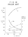
- the power supply circuits as shown in Figs. 9 and 10 configured to stabilize the secondary-side direct-current output voltage by the complex control method change the peak level of the parallel resonance voltage V1 according to load conditions and variation in the alternating input voltage VAC, as is shown in Figs. 13A to 13F and Fig. 14.
- the level of the alternating input voltage VAC as the 100-V commercial alternating-current power AC for example rises to 140 V under conditions of a heavy load approximating the maximum load power, in particular, the parallel resonance voltage V1 rises to 700 V at the maximum, as shown in Fig. 14.
- a product having a high withstand voltage selected for the switching device Q1 as described above increases power loss due to switching operation, and also reduces power conversion efficiency.
- a switching power supply circuit comprised as follows.
- the switching power supply circuit comprises a switching means including a main switching device for interrupting an inputted direct-current input voltage for output, a primary-side parallel resonant capacitor for forming a primary-side parallel resonant circuit that converts operation of the switching means into voltage resonance type operation, and an insulating converter transformer having a primary-side winding and a secondary-side winding for transmitting an output of the switching means obtained in the primary-side winding to the secondary-side winding, the primary-side winding and the secondary-side winding being wound so as to be loosely coupled to each other at a required coupling coefficient.
- the switching power supply circuit on the secondary side comprises a secondary-side resonant circuit formed by connecting a secondary-side resonant capacitor to the secondary-side winding, and a direct-current output voltage generating means for rectifying an alternating voltage inputted from the secondary-side winding and thereby providing a direct-current output voltage.
- the switching power supply circuit is characterized by further including an active clamp means for clamping a primary-side parallel resonance voltage generated across the primary-side parallel resonant capacitor during an off period of the main switching device, the active clamp means including an auxiliary switching device driven for switching operation by self-oscillation driving, and a switching driving means for effecting control for constant voltage by driving the main switching device for switching operation such that switching frequency of the main switching device is variably controlled according to level of the direct-current output voltage and an on/off period of the main switching device within one switching cycle is changed.
- the configuration on the primary side described above allows the active clamp means to clamp the parallel resonance voltage generated during the off period of the main switching device to thereby suppress the resonance voltage. Therefore, products having lower withstand voltage may be used for components such as the switching devices and the primary-side parallel resonant capacitor provided in the power supply circuit.
- the active clamp means is driven by a self-oscillation driving circuit of simple configuration that includes a driving winding formed by winding a wire of the primary-side winding of the insulating converter transformer. Therefore, the active clamp means requires only a small number of parts, and thus greatly contributes to miniaturization of the power supply circuit in particular.
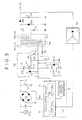
- Fig. 1 is a circuit configuration diagram of a power supply circuit according to a first embodiment of the present invention
- Fig. 3 is a circuit configuration diagram of a power supply circuit according to a second embodiment of the present invention.
- each of the power supply circuits shown in the figures is a complex resonance type switching converter provided with a voltage resonance type converter on the primary side and a resonant circuit on the secondary side. Therefore in this case, the power supply circuits each have an isolating converter transformer PIT configured as shown in Fig. 11. The same is true for power supply circuits according to other embodiments to be described later.
- the general primary-side configuration of the power supply circuit of Fig. 1 or Fig. 3 includes a voltage resonance type converter that has a main switching device Q1 and basically performs single-ended switching operation by being externally excited.
- the power supply circuit has an active clamp circuit 20 for clamping a parallel resonance voltage V1 across a parallel resonant capacitor Cr, which will be described later.
- a MOS-FET is used as the main switching device Q1 and as an auxiliary switching device Q2.
- a switching driver 10 is the same as in Fig. 9, for example, and specifically has an oscillating circuit 11 and a driving circuit 12.
- the oscillating circuit 11 generates an oscillating signal by changing its oscillating frequency according to change in a secondary-side direct-current output voltage E0 and changing duty ratio of its waveform within one switching cycle according to pulse level of the primary-side parallel resonance voltage V1, and then outputs the thus generated oscillating signal to the driving circuit 12 to drive the main switching device Q1.
- switching frequency of the main switching device Q1 is changed according to variation in load and variation in the alternating input voltage, and at the same time, its on/off period within one switching cycle is changed.
- control for constant voltage by the complex control method is effected by changing three parameters: the switching frequency of the main switching device Q1, and the on period and the off period within one switching cycle of the main switching device Q1.
- the active clamp circuit 20 in this case is formed with the auxiliary switching device Q2, a clamp capacitor CCL, and a clamp diode DD2.
- a so-called body diode, for example, is selected for the clamp diode DD2.
- a driving circuit system for driving the auxiliary switching device Q2 comprises the driving winding Ng, a capacitor Cg, and resistances R1 and R2.
- the clamp diode DD2 is connected in parallel with a drain and source of the auxiliary switching device Q2.
- an anode of the clamp diode DD2 is connected to the source of the auxiliary switching device Q2, while a cathode of the clamp diode DD2 is connected to the drain of the auxiliary switching device Q2.
- the drain of the auxiliary switching device Q2 is connected to one terminal of the clamp capacitor CCL, whereas the other terminal of the clamp capacitor CCL is connected to a node that connects a line of rectified and smoothed voltage Ei with a starting point of a primary winding N1.
- the source of the auxiliary switching device Q2 is connected to an ending point of the primary winding N1.
- the active clamp circuit 20 in the first and second embodiments is formed by connecting the clamp capacitor CCL in series with a parallel connection circuit of the auxiliary switching device Q2 and the clamp diode DD2.
- the circuit thus formed is connected in parallel with the primary winding N1 of the isolating converter transformer PIT.
- a series connection circuit of the resistance R1, the capacitor Cg, and the driving winding Ng included in the driving circuit system for driving the auxiliary switching device Q2 is connected to a gate of the auxiliary switching device Q2.
- the series connection circuit forms the self-oscillation driving circuit for driving the auxiliary switching device Q2.
- the driving winding Ng is formed by winding a wire on the ending point side of the primary winding N1 of the isolating converter transformer PIT, and the number of turns in this case is 1T (turn), for example.
- a voltage induced by an alternating voltage obtained in the primary winding N1 occurs in the driving winding Ng.
- the voltage obtained in the driving winding Ng is of opposite polarity from that of the primary winding N1. It is to be noted that when the number of turns of the driving winding Ng is 1T, operation of the driving winding Ng is insured in practice; however, the number of turns is not limited to 1T.
- the resistance R2 is inserted between nodes of the primary winding N1 of the isolating converter transformer PIT and the driving winding Ng.
- the power supply circuit is provided on the secondary side with a secondary-side parallel resonant circuit formed by a secondary winding N2 and a secondary-side resonant capacitor C2, and a half-wave rectifier circuit formed by a rectifier diode D0 and a smoothing capacitor C0 that is connected to a starting point side of the secondary winding N2.
- the power supply circuit is provided on the secondary side with a secondary-side series resonant circuit formed by a secondary winding N2 and a secondary-side series resonant capacitor C2, and a voltage doubler half-wave rectifier circuit formed by a set of rectifier diodes D01 and D02 and a smoothing capacitor C0. Either one of the half-wave rectifier circuits provides a secondary-side direct-current output voltage E0.
- Figs. 2A, 2B, 2C, 2D, 2E, 2F, 2G, 2H, 2I, 2J, 2K, 2L, 2M, 2N, 20, and 2P are waveform diagrams primarily showing switching operation on the primary side of the power supply circuit of Fig. 1. Specifically, the figures show operation of the voltage resonance type converter provided with the active clamp circuit 20. The operations shown in Figs. 2A to 2P are obtained when the circuit of Fig. 1 is configured for AC 100 V.
- the main switching device Q1 is controlled to be turned on during a period TON, and the auxiliary switching device Q2 is controlled so as to remain in an off state during the period TON.
- a switching output current I1 flows through the drain of the main switching device Q1 during the period TON.
- the switching output current I1 flows to the main switching device Q1 via leakage inductance L1 of the primary winding N1 of the isolating converter transformer PIT.
- the switching output current I1 in this period has a waveform that is initially reversed from a negative direction to a positive direction, as shown in the period TON in Fig. 2B.
- the clamp diode DD1 conducts and switching output current IQ1 flows through the clamp diode DD1 and the primary winding N1 after the parallel resonant capacitor Cr finishes discharging electricity at the end of an immediately preceding period td2.
- the main switching device Q1 In timing in which the switching output current I1 is reversed from a negative direction to a positive direction as shown in Fig. 2B, the main switching device Q1 is turned on by ZVS (Zero Volt Switching) and ZCS (Zero Current Switching).
- ZVS Zero Volt Switching
- ZCS Zero Current Switching
- the main switching device Q1 is turned off, whereby the current that has been flowing through the primary winding N1 flows to the parallel resonant capacitor Cr.
- the current Icr flowing through the parallel resonant capacitor Cr during this period exhibits a pulse-shaped waveform of positive polarity. This represents an operation in partial resonance mode.
- the main switching device Q1 is turned off by ZVS.
- auxiliary switching device Q2 is controlled so as to be in an on state, and the main switching device Q1 is controlled so as to be in an off state.
- This period corresponds to a period TON2 during which a voltage V2 across the auxiliary switching device Q2 shown in Fig. 2C is at a zero level.
- the period TON2 is a period of operation of the active clamp circuit 20, in which the active clamp circuit performs the following operation.
- the parallel resonant capacitor Cr is charged with the current flowing from the primary winding N1, whereby a voltage obtained at the primary winding N1 is at the same potential as or higher than the level of voltage across a clamp capacitor CCL1 at the start of the period TON2.
- capacitance of the clamp capacitor CCL1 is selected to be 50 times or more that of the parallel resonant capacitor Cr, for example, most of the current flows to the clamp capacitor CCL1 as the clamp current ICL, and little current flows to the parallel resonant capacitor Cr.
- the resonance voltage V1 in the prior art circuits of Figs. 9 and 10 has a level of 550 V, the resonance voltage V1 in the first and second embodiments is suppressed to 300 V.
- the clamp current ICL shown in Fig. 2E is reversed from a negative direction to a positive direction.
- the auxiliary switching device Q2 is turned on by ZVS and ZCS in timed relation to the reversal of the clamp current ICL from a negative direction to a positive direction.
- the clamp current ICL flows through the primary winding N1 and the clamp capacitor CCL, and then from the drain to the source of the auxiliary switching device Q2 while forming a waveform that increases in a positive direction as shown in Fig. 2E.
- a voltage applied to the gate of the auxiliary switching device Q2 is the voltage induced in the driving winding Ng, and forms a rectangular pulse waveform.
- a gate inflow current Ig flowing through the gate of the auxiliary switching device Q2 is made to flow so as to form a differential waveform as shown in Fig. 2D immediately after the end of the period td1 and during the period td2 by a differentiating circuit formed by the capacitor Cg and the resistance R2.
- the periods td1 and td2 are threshold periods during which both the main switching device Q1 and the auxiliary switching device Q2 are turned off; the threshold periods are retained by the flowing of the gate inflow current Ig.
- a period TOFF is ended when the voltage V2 across the auxiliary switching device Q2, which has been at a zero level during the period TOFF because the auxiliary switching device Q2 has been turned on, begins to rise. Then, the parallel resonant capacitor Cr discharges a current into the primary winding N1. This represents a partial resonance operation.
- the gradient of the parallel resonance voltage V1 applied to the main switching device Q1 in this period is steep because of the small capacitance of the parallel resonant capacitor Cr. Thus, as shown in Fig. 2A, the parallel resonance voltage V1 falls rapidly to a zero level.
- the turning-off of the auxiliary switching device Q2 begins.
- the auxiliary switching device Q2 is turned off by ZVS.
- a voltage generated by turning off the auxiliary switching device Q2 does not rise steeply because of the discharge of the parallel resonant capacitor Cr.
- This operation is for example shown in Fig. 2C as the voltage V2 across the auxiliary switching device Q2, which voltage has a waveform that makes a transition from a zero level to a peak level with a certain gradient in the period td2,
- the voltage V2 across the auxiliary switching device Q2 has a level of 300 V for example during a period TOFF2 during which the auxiliary switching device Q2 is turned off, then makes a transition from 300 V to a zero level during the period td1, which is a starting period of the period TOFF2, and, as described above, makes a transition from the zero level to 300 V during the period td2, which is an ending period of the period TOFF2. Thereafter, the operation described above is repeated for each switching cycle.
- Fig. 2G shows a secondary-side alternating voltage V3 across the secondary-side parallel or series resonant capacitor C2
- Fig. 2H shows a secondary-side rectified current Io flowing in the secondary-side rectifier diode D0.
- the secondary-side alternating voltage V3 is clamped at the level of the secondary-side direct-current voltage E0 during a period DON during which the secondary-side rectifier diode D01 conducts and therefore is in an on state, and shows a sinusoidal waveform that has a peak in a direction of negative polarity during a period DOFF during which the secondary-side rectifier diode D01 is in an off state.
- the secondary-side rectified current I0 is at a zero level during the period DOFF, and flows in a manner shown by a waveform in Fig. 2H during the period DON.
- a comparison of the primary-side parallel resonance voltages V1 in Figs. 2A and 2I indicates that a waveform shown in Fig. 2I has a noticeably shorter period TON, during which the main switching device Q1 is turned on, as compared with Fig. 2A.
- the switching frequency of Fig. 2I is higher than that of Fig. 2A at the maximum load power. It is to be noted that the period TOFF during which the main switching device Q1 is turned off is actually slightly changed.
- the main switching device Q1 on the primary side is controlled so as to raise its switching frequency as the load power is decreased and the secondary-side output voltage E0 is raised, and that at the same time, the on/off period within one switching cycle of the main switching device Q1 is variably controlled.
- an operation for constant voltage by the complex control method that variably controls the three parameters mentioned above: the switching frequency fs, the period TON, and the period TOFF is indicated.
- the auxiliary switching device Q2 is driven in timing in accordance with the waveform of the voltage obtained in the driving winding Ng.
- the voltage obtained in the driving winding Ng is induced by the alternating voltage occurring in the primary winding N1. Accordingly, in synchronism with the switching operation of the main switching device Q1 controlled in a manner described above, the on period TON2 and the off period TOFF2 of the auxiliary switching device Q2 are changed. Thus, the switching frequency of the auxiliary switching device Q2 is also variably controlled.
- the on/off period of the auxiliary switching device Q2 is also variably controlled according as the on/off period of the main switching device Q1 is changed. This is because the level of the voltage for driving the auxiliary switching device Q2 is varied as the voltage induced in the driving winding Ng is changed according to load variation and variation in the rectified and smoothed voltage Ei.
- a product having a low on resistance of 400 V/10 A is selected for the main switching device Q1, and a product having a low on resistance of 400 V/3 A is selected for the auxiliary switching device Q2.
- variable switching frequency fs The range of the variable switching frequency fs to be set when these components are selected is 100 KHz to 150 KHz, for example.
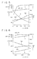
- Fig. 5 shows relations of power conversion efficiency ⁇ DC ⁇ DC, the switching frequency fs and the periods TON and TOFF of the main switching device Q1 with respect to load power Po.
- PWM control is effected such that the period TON during which the main switching device Q1 is turned on is lengthened as the load power becomes heavier, and at the same time, the period TOFF during which the main switching device Q1 is turned off is also lengthened though in smaller degrees than the period TON.
- the switching frequency fs is controlled to decrease.
- the parallel resonance voltage V1 is suppressed to a region of 600 V.
- the period TON during which the main switching device Q1 is turned on is controlled to be shortened as the rectified and smoothed voltage Ei is raised, and at the same time, the period TOFF during which the main switching device Q1 is turned off is lengthened with a gentle gradient.
- the switching frequency fs is controlled to rise as the rectified and smoothed voltage Ei is raised.
- a power conversion efficiency of 94 percent or more is retained irrespective of change in the rectified and smoothed voltage Ei.
- the circuit shown in Fig. 1 clamps the parallel resonance voltage V1 generated during the off period of the main switching device Q1 to suppress its level.
- the parallel resonance voltage V1 can be suppressed to about 300 V.
- Even in the case of AC 200 V it is possible to suppress the maximum value of peak level of the parallel resonance voltage V1 to about 600 V in normal operation.
- a product having a withstand voltage of 400 V may be selected for AC 100 V
- a product having a withstand voltage of 800 V may be selected for AC 200 V. It is therefore possible to use a product having a lower withstand voltage than those of the circuits shown in Figs. 9 and 10.
- a product having an equally low withstand voltage may be used for the auxiliary switching device Q2.
- characteristics of the switching devices of the circuit shown in Fig. 1 are improved over those of the circuits shown in Figs. 9 and 10.
- the switching device is a MOS-FET
- its on resistance is-reduced, thereby resulting in an improvement in power conversion efficiency.
- the first and second embodiments perform an operation by the complex control method that variably controls the three parameters mentioned above: the switching frequency fs, the on period, and the off period of the switching device, thereby extending a range of control for constant voltage.
- the switching device can be miniaturized. For example, products having a withstand voltage of 1000 V or higher are required as the switching devices for use in the circuits of Figs. 9 and 10, thus resulting in relatively large package size. On the other hand, smaller package products may be used as the switching devices Q1 and Q2 in the circuit of Fig. 1.
- the parallel resonant capacitor Cr since the level of the parallel resonance voltage V1 is suppressed, a product having a lower withstand voltage than those of the circuits of Figs. 9 and 10 may be employed as the parallel resonant capacitor Cr in the circuit of Fig. 1. Thus, the parallel resonant capacitor Cr can also be miniaturized.
- the power supply circuit shown in Fig. 1 variably controls the switching frequency of the primary-side switching converter according to variation in load power, the power supply circuit operates so as to lower the switching frequency when a short circuit in the load occurs.
- the circuits of Figs. 9 and 10 lower the switching frequency and thereby lengthen the on period of the switching device when a short circuit in the load occurs, and accordingly the voltage applied to the switching device and the parallel resonant capacitor is increased.
- the power supply circuits need to be provided with a protection circuit for protecting the switching device by limiting a high level of voltage and current generated at the time of the short circuit in the load.
- the power supply circuits according to the first and second embodiments change the parallel resonance voltage V1 only in small degrees according to load variation, and therefore the rise of the parallel resonance voltage V1 is controlled even when the switching frequency is lowered at the time of the short circuit in the load. It is thereby possible to omit a protection circuit to deal with the short circuit in the load.
- the first and second embodiments are particularly characterized by including the self-oscillation driving circuit system comprising the driving winding Ng, the capacitor Cg, and the resistances R1 and R2 for driving the auxiliary switching device Q2 in the active clamp circuit 20 for switching operation.
- an external oscillation driving circuit system for driving the auxiliary switching device Q2 by complex control may be additionally provided in the switching driver 10.
- both the main switching device Q1 and the auxiliary switching device Q2 are driven by a circuit such as an externally oscillating IC.
- a circuit such as an externally oscillating IC.
- the circuit system for driving the auxiliary switching device Q2 has a very simple circuit configuration including the winding of only 1T wound in the isolating converter transformer PIT, the two resistances, and the single capacitor, and realizes the same operation as the external oscillation driving circuit system does.
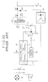
- Fig. 7 is a circuit configuration diagram of a power supply circuit according to a third embodiment of the present invention
- Fig. 8 is a circuit configuration diagram of a power supply circuit according to a fourth embodiment of the present invention.
- the same parts as in Fig. 1 are identified by the same reference numerals, and their description will be omitted.
- an IGBT Insulated Gate Bipolar Transistor
- two rectifier diodes D01 and D02 and two smoothing capacitors C01 and C02 are connected to a secondary-side parallel resonant circuit in a manner shown in the figure to thereby form a voltage doubler rectifier circuit.
- a voltage obtained between a positive terminal of the smoothing capacitor C01 and a secondary-side ground, that is, a secondary-side direct-current voltage E0 has a level twice that of an alternating voltage obtained in a secondary winding N2.
- the number of turns of the secondary winding N2 may be reduced to 1/2, thereby making it possible to miniaturize the isolating converter transformer PIT as much, for example.
- the resonant circuit on the secondary side is not limited to the configurations shown in the figures, a secondary-side series resonant circuit as in Fig. 3 may be employed.
- embodiments of the present invention are not limited to the configurations shown in the drawings.
- MOS-FETs, BJTs (Bipolar Junction Transistors) or IGBTs are used as the main switching device and the auxiliary switching device; however, other devices such as SITs (Static Induction Thyristors) may also be employed.
- configuration of the switching driver for driving the main switching device Q1 by external oscillation does not need to be limited to those shown in the drawings; it may be modified into an appropriate circuit configuration as required.
- the rectifier circuit on the secondary side including the secondary-side resonant circuit is not limited to the configurations shown in the drawings as embodiments of the present invention; the rectifier circuit may employ different circuit configurations.
Landscapes
- Engineering & Computer Science (AREA)
- Power Engineering (AREA)
- Dc-Dc Converters (AREA)
- Inverter Devices (AREA)
Applications Claiming Priority (4)
| Application Number | Priority Date | Filing Date | Title |
|---|---|---|---|
| JP2000149815 | 2000-05-17 | ||
| JP2000149815A JP4501224B2 (ja) | 2000-05-17 | 2000-05-17 | スイッチング電源回路 |
| JP2000164768 | 2000-05-30 | ||
| JP2000164768A JP2001339948A (ja) | 2000-05-30 | 2000-05-30 | スイッチング電源回路 |
Publications (2)
| Publication Number | Publication Date |
|---|---|
| EP1156580A2 true EP1156580A2 (fr) | 2001-11-21 |
| EP1156580A3 EP1156580A3 (fr) | 2004-01-14 |
Family
ID=26592313
Family Applications (1)
| Application Number | Title | Priority Date | Filing Date |
|---|---|---|---|
| EP01304310A Withdrawn EP1156580A3 (fr) | 2000-05-17 | 2001-05-15 | Appareil d'alimentation de puisance à découpage |
Country Status (5)
| Country | Link |
|---|---|
| US (1) | US6366476B1 (fr) |
| EP (1) | EP1156580A3 (fr) |
| KR (1) | KR20010106228A (fr) |
| CN (1) | CN1324141A (fr) |
| TW (1) | TW521481B (fr) |
Cited By (9)
| Publication number | Priority date | Publication date | Assignee | Title |
|---|---|---|---|---|
| EP1684405A2 (fr) * | 2005-01-25 | 2006-07-26 | Sony Corporation | Circuit d'alimentation à découpage |
| EP1772950A2 (fr) * | 2005-10-07 | 2007-04-11 | Sony Corporation | Circuit d'alimentation à découpage |
| WO2007138344A2 (fr) * | 2006-05-26 | 2007-12-06 | Cambridge Semiconductor Limited | Convertisseurs et contrôleurs d'énergie d'avancement |
| WO2009068930A1 (fr) * | 2007-11-28 | 2009-06-04 | Thomson Licensing | Alimentation électrique |
| US7570497B2 (en) | 2006-05-26 | 2009-08-04 | Cambridge Semiconductor | Discontinuous quasi-resonant forward converter |
| US7738266B2 (en) | 2006-05-26 | 2010-06-15 | Cambridge Semiconductor Limited | Forward power converter controllers |
| CN102315782A (zh) * | 2010-07-08 | 2012-01-11 | 晶宏半导体股份有限公司 | 无需电解电容的电源转换器及其电源转换方法 |
| DE102015102507B4 (de) * | 2014-02-28 | 2016-09-15 | Panasonic Intellectual Property Management Co., Ltd. | Stromversorgungseinrichtung und diese verwendende Beleuchtungsvorrichtung |
| EP2573924B1 (fr) * | 2006-09-13 | 2019-02-27 | Cree, Inc. | Circuit pour alimenter en énergie électrique |
Families Citing this family (63)
| Publication number | Priority date | Publication date | Assignee | Title |
|---|---|---|---|---|
| JP2002064980A (ja) * | 2000-08-16 | 2002-02-28 | Sony Corp | スイッチング電源回路 |
| JP3659240B2 (ja) * | 2001-11-16 | 2005-06-15 | ソニー株式会社 | スイッチング電源回路 |
| JP3557198B2 (ja) * | 2002-06-17 | 2004-08-25 | 株式会社東芝 | スイッチング電源回路及び電子機器 |
| WO2005011094A1 (fr) * | 2003-07-24 | 2005-02-03 | Sanken Electric Co., Ltd. | Convertisseur c.c. |
| US7106602B2 (en) * | 2003-07-29 | 2006-09-12 | Astec International Limited | Switching-bursting method and apparatus for reducing standby power and improving load regulation in a DC—DC converter |
| US7239531B2 (en) * | 2004-03-18 | 2007-07-03 | Fairchild Semiconductor Corporation | Resonant lossless circuit for providing a low operating voltage in power converter |
| JP3693061B1 (ja) * | 2004-03-26 | 2005-09-07 | サンケン電気株式会社 | スイッチング電源装置 |
| US8581147B2 (en) * | 2005-03-24 | 2013-11-12 | Lincoln Global, Inc. | Three stage power source for electric ARC welding |
| US9956639B2 (en) * | 2005-02-07 | 2018-05-01 | Lincoln Global, Inc | Modular power source for electric ARC welding and output chopper |
| US8785816B2 (en) * | 2004-07-13 | 2014-07-22 | Lincoln Global, Inc. | Three stage power source for electric arc welding |
| US8269141B2 (en) * | 2004-07-13 | 2012-09-18 | Lincoln Global, Inc. | Power source for electric arc welding |
| CN100459391C (zh) * | 2004-07-14 | 2009-02-04 | 伊博电源(杭州)有限公司 | 一种开关电源的自驱动电路 |
| JP4099595B2 (ja) * | 2004-09-30 | 2008-06-11 | ソニー株式会社 | スイッチング電源回路 |
| JP4506469B2 (ja) * | 2005-01-06 | 2010-07-21 | サンケン電気株式会社 | 共振型電源装置 |
| JP2006191746A (ja) * | 2005-01-06 | 2006-07-20 | Sony Corp | スイッチング電源回路 |
| JP4360326B2 (ja) * | 2005-01-21 | 2009-11-11 | サンケン電気株式会社 | 共振型スイッチング電源装置 |
| JP2006217747A (ja) * | 2005-02-04 | 2006-08-17 | Sony Corp | スイッチング電源回路 |
| US9855620B2 (en) | 2005-02-07 | 2018-01-02 | Lincoln Global, Inc. | Welding system and method of welding |
| JP4701749B2 (ja) * | 2005-02-25 | 2011-06-15 | サンケン電気株式会社 | 直流変換装置 |
| US7339801B2 (en) * | 2005-04-08 | 2008-03-04 | Sony Corporation | Switching power supply circuit |
| US9647555B2 (en) | 2005-04-08 | 2017-05-09 | Lincoln Global, Inc. | Chopper output stage for arc welder power source |
| JP2006345633A (ja) * | 2005-06-08 | 2006-12-21 | Sony Corp | スイッチング電源回路 |
| EP1744440A3 (fr) * | 2005-06-30 | 2009-04-15 | Sony Corporation | Circuit d'alimentation de puissance à découpage |
| TWI297977B (en) * | 2005-07-05 | 2008-06-11 | Delta Electronics Inc | Soft switching dc-dc converter |
| TW200721653A (en) * | 2005-09-02 | 2007-06-01 | Sony Corp | Switching power supply circuit |
| KR100721432B1 (ko) * | 2005-09-26 | 2007-05-25 | 학교법인 포항공과대학교 | 전파출력 직렬공진회로를 이용한 능동 클램프회로 |
| JP4774903B2 (ja) * | 2005-10-17 | 2011-09-21 | サンケン電気株式会社 | スイッチング電源装置 |
| TWI301351B (en) * | 2005-10-31 | 2008-09-21 | Delta Electronics Inc | Switching power supply and zvs method thereof |
| CN1992493B (zh) * | 2005-12-30 | 2011-05-18 | 艾默生网络能源系统北美公司 | 一种谐振直流/直流变换器及其控制方法 |
| US20100202167A1 (en) * | 2009-02-10 | 2010-08-12 | System General Corp. | Soft switching power converter with a variable switching frequency for improving operation and efficiency |
| CN101834063B (zh) * | 2009-03-11 | 2012-05-30 | 王京申 | 一种用于自激式开关电源变换器的脉冲驱动变压器组件 |
| SE534975C2 (sv) * | 2009-10-16 | 2012-03-06 | Tsc Innovation Ab | Förfarande vid och anordning för installation och reparation av isolerade ledningsrör |
| TWI426694B (zh) * | 2010-04-02 | 2014-02-11 | System General Corp | 柔性切換式功率轉換器 |
| US20110305048A1 (en) * | 2010-06-11 | 2011-12-15 | System General Corp. | Active-clamp circuit for quasi-resonant flyback power converter |
| US8743523B2 (en) | 2010-07-28 | 2014-06-03 | General Electric Company | Systems, methods, and apparatus for limiting voltage across a switch |
| CN103339822B (zh) | 2011-01-19 | 2016-05-18 | 株式会社泰库诺瓦 | 非接触供电系统 |
| DE102011104441A1 (de) * | 2011-06-16 | 2012-12-20 | Fujitsu Technology Solutions Intellectual Property Gmbh | Schaltnetzteil, Betriebsverfahren und Verwendung eines Schaltnetzteils in einem Computer |
| US8743565B2 (en) * | 2012-07-27 | 2014-06-03 | Flextronics Ap, Llc | High power converter architecture |
| US9605860B2 (en) | 2012-11-02 | 2017-03-28 | Flextronics Ap, Llc | Energy saving-exhaust control and auto shut off system |
| US9660540B2 (en) | 2012-11-05 | 2017-05-23 | Flextronics Ap, Llc | Digital error signal comparator |
| US9494658B2 (en) | 2013-03-14 | 2016-11-15 | Flextronics Ap, Llc | Approach for generation of power failure warning signal to maximize useable hold-up time with AC/DC rectifiers |
| US9323267B2 (en) | 2013-03-14 | 2016-04-26 | Flextronics Ap, Llc | Method and implementation for eliminating random pulse during power up of digital signal controller |
| US9627915B2 (en) | 2013-03-15 | 2017-04-18 | Flextronics Ap, Llc | Sweep frequency mode for multiple magnetic resonant power transmission |
| KR102116705B1 (ko) * | 2013-10-16 | 2020-06-05 | 온세미컨덕터코리아 주식회사 | 컨버터 및 그 구동 방법 |
| CN104578787B (zh) * | 2013-10-17 | 2017-11-10 | 南京博兰得电子科技有限公司 | 谐振电源转换装置及其控制方法 |
| US20150263639A1 (en) | 2014-03-14 | 2015-09-17 | Avogy, Inc. | Adaptive synchronous switching in a resonant converter |
| WO2015138880A1 (fr) * | 2014-03-14 | 2015-09-17 | Avogy, Inc. | Commutation synchrone adaptative dans un convertisseur résonant |
| TWI513164B (zh) * | 2014-04-18 | 2015-12-11 | Lite On Technology Corp | 返馳式主動箝位電源轉換器 |
| CN105337503B (zh) * | 2014-06-25 | 2017-12-01 | 光宝电子(广州)有限公司 | 直流电压转换装置及适用于直流电压转换装置的箝位电路 |
| US9906137B2 (en) * | 2014-09-23 | 2018-02-27 | Cree, Inc. | High power density, high efficiency power electronic converter |
| FR3046854B1 (fr) * | 2016-01-14 | 2019-07-12 | Sagem Defense Securite | Procede d'asservissement d'un convertisseur de tension continue-continue |
| JP6382885B2 (ja) * | 2016-05-23 | 2018-08-29 | 双葉電子工業株式会社 | 電源装置 |
| CN107196517B (zh) * | 2017-07-04 | 2019-07-19 | 广州金升阳科技有限公司 | 开关电源中钳位开关的驱动电路 |
| TWI652890B (zh) | 2017-07-27 | 2019-03-01 | 群光電能科技股份有限公司 | 具箝位模式切換之電源轉換系統 |
| US10553339B1 (en) * | 2018-03-30 | 2020-02-04 | Universal Lighting Technologies, Inc. | Common-mode choke with integrated RF inductor winding |
| CN112117905B (zh) * | 2019-06-20 | 2021-12-21 | 东南大学 | 有源钳位反激变换器的控制系统及方法 |
| US11114945B2 (en) * | 2019-08-22 | 2021-09-07 | Cypress Semiconductor Corporation | Secondary-controlled active clamp implementation for improved efficiency |
| CN111584205A (zh) * | 2020-06-10 | 2020-08-25 | 中车株洲电机有限公司 | 一种电力电子变压器及变压器绝缘电位分布结构 |
| CN112615531A (zh) * | 2020-12-14 | 2021-04-06 | 矽力杰半导体技术(杭州)有限公司 | 控制电路以及应用其的开关变换器 |
| US11716015B2 (en) * | 2021-02-11 | 2023-08-01 | Rockwell Automation Technologies, Inc. | Low quiescent current startup circuit |
| TWI800203B (zh) * | 2022-01-04 | 2023-04-21 | 捷拓科技股份有限公司 | 自激式主動箝位電路 |
| US11990841B2 (en) | 2022-03-08 | 2024-05-21 | Minmax Technology Co., Ltd. | Multi-mode hybrid control DC-DC converting circuit and control method thereof |
| US11936287B2 (en) | 2022-03-08 | 2024-03-19 | Minmax Technology Co., Ltd. | Self-driven active clamp circuit |
Citations (6)
| Publication number | Priority date | Publication date | Assignee | Title |
|---|---|---|---|---|
| US4736283A (en) * | 1985-09-13 | 1988-04-05 | Sony Corporation | Regulated voltage converter which has substantially fewer parts than prior art devices |
| EP0404191A2 (fr) * | 1989-06-23 | 1990-12-27 | Matsushita Electric Industrial Co., Ltd. | Dispositif d'alimentation de puissance à découpage |
| EP0766372A2 (fr) * | 1995-09-26 | 1997-04-02 | Nec Corporation | Convertisseur résonant courant continu-courant continu contrÔlable par modulation de largeur d'impulsion |
| US5991171A (en) * | 1998-02-05 | 1999-11-23 | Pi Electronics (H.K.) Ltd. | DC-to-DC converters |
| US5991170A (en) * | 1998-02-03 | 1999-11-23 | Sony Corporation | Equipment and method for transmitting electric power |
| US6061252A (en) * | 1997-12-22 | 2000-05-09 | Murata Manufacturing Co., Ltd. | Switching power supply device |
Family Cites Families (4)
| Publication number | Priority date | Publication date | Assignee | Title |
|---|---|---|---|---|
| US3742371A (en) * | 1971-12-16 | 1973-06-26 | Tektronix Inc | Wide range regulated power supply utilizing optimized energy storage |
| KR940005058B1 (ko) * | 1992-02-14 | 1994-06-10 | 삼성전자 주식회사 | 전자레인지의 출력안정화회로 및 그 방법 |
| JPH08168249A (ja) * | 1994-10-11 | 1996-06-25 | Sony Corp | 電流共振形スイッチング電源回路 |
| JPH09131051A (ja) * | 1995-10-31 | 1997-05-16 | Sony Corp | 力率改善コンバータ回路 |
-
2001
- 2001-05-01 TW TW090110423A patent/TW521481B/zh not_active IP Right Cessation
- 2001-05-10 KR KR1020010025377A patent/KR20010106228A/ko not_active Application Discontinuation
- 2001-05-15 EP EP01304310A patent/EP1156580A3/fr not_active Withdrawn
- 2001-05-15 US US09/855,247 patent/US6366476B1/en not_active Expired - Fee Related
- 2001-05-17 CN CN01117781A patent/CN1324141A/zh active Pending
Patent Citations (6)
| Publication number | Priority date | Publication date | Assignee | Title |
|---|---|---|---|---|
| US4736283A (en) * | 1985-09-13 | 1988-04-05 | Sony Corporation | Regulated voltage converter which has substantially fewer parts than prior art devices |
| EP0404191A2 (fr) * | 1989-06-23 | 1990-12-27 | Matsushita Electric Industrial Co., Ltd. | Dispositif d'alimentation de puissance à découpage |
| EP0766372A2 (fr) * | 1995-09-26 | 1997-04-02 | Nec Corporation | Convertisseur résonant courant continu-courant continu contrÔlable par modulation de largeur d'impulsion |
| US6061252A (en) * | 1997-12-22 | 2000-05-09 | Murata Manufacturing Co., Ltd. | Switching power supply device |
| US5991170A (en) * | 1998-02-03 | 1999-11-23 | Sony Corporation | Equipment and method for transmitting electric power |
| US5991171A (en) * | 1998-02-05 | 1999-11-23 | Pi Electronics (H.K.) Ltd. | DC-to-DC converters |
Cited By (16)
| Publication number | Priority date | Publication date | Assignee | Title |
|---|---|---|---|---|
| EP1684405A2 (fr) * | 2005-01-25 | 2006-07-26 | Sony Corporation | Circuit d'alimentation à découpage |
| EP1684405A3 (fr) * | 2005-01-25 | 2008-02-06 | Sony Corporation | Circuit d'alimentation à découpage |
| EP1772950A3 (fr) * | 2005-10-07 | 2009-07-08 | Sony Corporation | Circuit d'alimentation à découpage |
| EP1772950A2 (fr) * | 2005-10-07 | 2007-04-11 | Sony Corporation | Circuit d'alimentation à découpage |
| US7738266B2 (en) | 2006-05-26 | 2010-06-15 | Cambridge Semiconductor Limited | Forward power converter controllers |
| WO2007138344A3 (fr) * | 2006-05-26 | 2008-11-13 | Cambridge Semiconductor Ltd | Convertisseurs et contrôleurs d'énergie d'avancement |
| US7570497B2 (en) | 2006-05-26 | 2009-08-04 | Cambridge Semiconductor | Discontinuous quasi-resonant forward converter |
| WO2007138344A2 (fr) * | 2006-05-26 | 2007-12-06 | Cambridge Semiconductor Limited | Convertisseurs et contrôleurs d'énergie d'avancement |
| EP2573924B1 (fr) * | 2006-09-13 | 2019-02-27 | Cree, Inc. | Circuit pour alimenter en énergie électrique |
| EP2573923B1 (fr) * | 2006-09-13 | 2019-04-03 | Cree, Inc. | Circuit pour alimenter en énergie électrique |
| WO2009068930A1 (fr) * | 2007-11-28 | 2009-06-04 | Thomson Licensing | Alimentation électrique |
| US8482939B2 (en) | 2007-11-28 | 2013-07-09 | Thomson Licensing | Power supply |
| KR101359248B1 (ko) * | 2007-11-28 | 2014-02-05 | 톰슨 라이센싱 | 전원 |
| CN102315782A (zh) * | 2010-07-08 | 2012-01-11 | 晶宏半导体股份有限公司 | 无需电解电容的电源转换器及其电源转换方法 |
| CN102315782B (zh) * | 2010-07-08 | 2013-10-16 | 晶宏半导体股份有限公司 | 无需电解电容的电源转换器及其电源转换方法 |
| DE102015102507B4 (de) * | 2014-02-28 | 2016-09-15 | Panasonic Intellectual Property Management Co., Ltd. | Stromversorgungseinrichtung und diese verwendende Beleuchtungsvorrichtung |
Also Published As
| Publication number | Publication date |
|---|---|
| EP1156580A3 (fr) | 2004-01-14 |
| CN1324141A (zh) | 2001-11-28 |
| US6366476B1 (en) | 2002-04-02 |
| KR20010106228A (ko) | 2001-11-29 |
| US20020021575A1 (en) | 2002-02-21 |
| TW521481B (en) | 2003-02-21 |
Similar Documents
| Publication | Publication Date | Title |
|---|---|---|
| US6366476B1 (en) | Switching power supply apparatus with active clamp circuit | |
| EP1150418B1 (fr) | Appareil d'alimentation de puissance à découpage avec circuit actif de verrouillage de tension | |
| JP5088386B2 (ja) | スイッチング電源装置 | |
| US6396717B2 (en) | Switching power supply having an improved power factor by voltage feedback | |
| US6349046B2 (en) | Switching power supply circuit | |
| EP1124316A2 (fr) | Circuit de puissance à découpage | |
| JP2000152617A (ja) | スイッチング電源回路 | |
| JP2005073335A (ja) | スイッチング電源回路 | |
| JP2002262568A (ja) | スイッチング電源回路 | |
| JP2002262567A (ja) | スイッチング電源回路 | |
| JP4501224B2 (ja) | スイッチング電源回路 | |
| JP4367611B2 (ja) | スイッチング電源回路 | |
| JP2001339948A (ja) | スイッチング電源回路 | |
| JP4218092B2 (ja) | スイッチング電源回路 | |
| JP2001275350A (ja) | スイッチング電源回路 | |
| JP4264625B2 (ja) | スイッチング電源回路 | |
| JP3528816B2 (ja) | スイッチング電源回路 | |
| JP2001224171A (ja) | スイッチング電源回路 | |
| JP2000125552A (ja) | 電圧共振形スイッチング電源回路 | |
| JP2000125555A (ja) | 電圧共振形スイッチング電源回路 | |
| JP2003189614A (ja) | スイッチング電源回路 | |
| JP2002136139A (ja) | スイッチング電源回路 | |
| JP2000125559A (ja) | 電圧共振形スイッチング電源回路 | |
| JP2000125554A (ja) | 電圧共振形スイッチング電源回路 | |
| JP2002272103A (ja) | スイッチング電源回路 |
Legal Events
| Date | Code | Title | Description |
|---|---|---|---|
| PUAI | Public reference made under article 153(3) epc to a published international application that has entered the european phase |
Free format text: ORIGINAL CODE: 0009012 |
|
| AK | Designated contracting states |
Kind code of ref document: A2 Designated state(s): AT BE CH CY DE DK ES FI FR GB GR IE IT LI LU MC NL PT SE TR |
|
| AX | Request for extension of the european patent |
Free format text: AL;LT;LV;MK;RO;SI |
|
| PUAL | Search report despatched |
Free format text: ORIGINAL CODE: 0009013 |
|
| AK | Designated contracting states |
Kind code of ref document: A3 Designated state(s): AT BE CH CY DE DK ES FI FR GB GR IE IT LI LU MC NL PT SE TR |
|
| AX | Request for extension of the european patent |
Extension state: AL LT LV MK RO SI |
|
| AKX | Designation fees paid | ||
| REG | Reference to a national code |
Ref country code: DE Ref legal event code: 8566 |
|
| STAA | Information on the status of an ep patent application or granted ep patent |
Free format text: STATUS: THE APPLICATION IS DEEMED TO BE WITHDRAWN |
|
| 18D | Application deemed to be withdrawn |
Effective date: 20040715 |