EP1154553A2 - Schaltung und Verfahren zur Synchronisierung von parallelgeschalteten spannungsgespeisten Wechselrichtern - Google Patents
Schaltung und Verfahren zur Synchronisierung von parallelgeschalteten spannungsgespeisten Wechselrichtern Download PDFInfo
- Publication number
- EP1154553A2 EP1154553A2 EP01302905A EP01302905A EP1154553A2 EP 1154553 A2 EP1154553 A2 EP 1154553A2 EP 01302905 A EP01302905 A EP 01302905A EP 01302905 A EP01302905 A EP 01302905A EP 1154553 A2 EP1154553 A2 EP 1154553A2
- Authority
- EP
- European Patent Office
- Prior art keywords
- signal
- inverter circuit
- phase
- circuit
- sampling
- Prior art date
- Legal status (The legal status is an assumption and is not a legal conclusion. Google has not performed a legal analysis and makes no representation as to the accuracy of the status listed.)
- Granted
Links
Images
Classifications
-
- H—ELECTRICITY
- H02—GENERATION; CONVERSION OR DISTRIBUTION OF ELECTRIC POWER
- H02M—APPARATUS FOR CONVERSION BETWEEN AC AND AC, BETWEEN AC AND DC, OR BETWEEN DC AND DC, AND FOR USE WITH MAINS OR SIMILAR POWER SUPPLY SYSTEMS; CONVERSION OF DC OR AC INPUT POWER INTO SURGE OUTPUT POWER; CONTROL OR REGULATION THEREOF
- H02M7/00—Conversion of AC power input into DC power output; Conversion of DC power input into AC power output
- H02M7/42—Conversion of DC power input into AC power output without possibility of reversal
- H02M7/44—Conversion of DC power input into AC power output without possibility of reversal by static converters
- H02M7/48—Conversion of DC power input into AC power output without possibility of reversal by static converters using discharge tubes with control electrode or semiconductor devices with control electrode
- H02M7/493—Conversion of DC power input into AC power output without possibility of reversal by static converters using discharge tubes with control electrode or semiconductor devices with control electrode the static converters being arranged for operation in parallel
Definitions
- the present invention relates generally to voltage source inverters, and more specifically, to a synchronization circuit for synchronizing the output of parallel voltage source inverters.
- each of the voltage source inverters has an associated phase angle.
- One known problem with placing voltage source inverters in parallel is that if the phase angles are not the same in each of the parallel voltage source inverters, circulating real power between the voltage sources may be developed. Circulating real power reduces the capability and efficiency of the voltage sources. Further, circulating real power may also cause the malfunctioning of the voltage source inverter.
- the parallel voltage source inverters essentially become electrically equivalent by the present invention to eliminate the circulating real power.
- an inverter circuit comprises a synchronization signal source having a first frequency and a first phase.
- a first voltage source inverter circuit is coupled to a load and the synch source.
- the first voltage source inverter circuit comprises a cycle time counter generating a cyclic output signal and a first sampling circuit receiving the cyclic output signal and sampling said cyclic output signal.
- the first sampling circuit generates a magnitude signal and a phase signal in response to said cyclic output signal.
- the first inverter circuit generates an output signal having a first phase in response to the magnitude signal and the phase signal.
- a second voltage source inverter circuit is coupled to the load in parallel with the first voltage source inverter and to the synch signal source.
- the second voltage source inverter circuit has a second cycle time counter generating a second cyclic output signal.
- the second sampling circuit receives the second cyclic output signal and samples the second cyclic output signal.
- the second sampling circuit generates a second magnitude signal and a second phase signal in response to the cyclic output signal.
- the second phase signal and the first phase signal are substantially synchronised.
- a method for generating a voltage signal using a first inverter circuit in parallel with the second inverter circuit comprises the steps of:
- a sawtooth generator may be used to generate the cyclic output signal that represents the phase angle. This eliminates the usually strict requirement that the updating rate of each of the voltage source inverters must be the same and that the updating cycle must be synchronized for the phase angle synchronization among the voltage source inverters.
- Another advantage of the invention is that the fundamental operating frequency and the sampling frequency of the microprocessor do not need strict synchronization.
- Another advantage of the invention is that no analog-to-digital conversion is required between the microcontroller and the sawtooth wave generator.
- the synchronous signal source is digital which has much better noise immunity than analog signals. Also, the digital signal is based on a relatively low frequency and thus the bandwidth requirements for transmission among the parallel voltage source inverters is low.
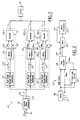
- an inverter circuit 10 has a synchronization (synch) signal source 12 coupled to a plurality of voltage source inverter circuits (VSI 1, VSI n-1, and VSI n). Although three voltage source inverter circuits (VSI) are illustrated, various numbers of voltage source inverter circuits may be used depending on the output power to be provided as would be evident to those skilled in the art.
- the output of each voltage source inverter circuit VSI 1, VSI n-1, and VSI n is coupled to a common load 14.
- Synch signal source 12 is illustrated as a square wave generator. However, those skilled in the art would recognize that other types of synch signal sources may be used. Synch signal source 12 has a fundamental operating frequency input 16. A suitable fundamental operating frequency is a relatively low frequency, e.g., preferably about 50 or 60 Hz. The preferred fundamental operating frequency is the frequency provided through the connection to the mains power companies.
- the synch signal source 12 generates a synch signal represented by reference numeral 18 through an output 20.
- the synch signal 18 has a first frequency corresponding to the fundamental operating frequency input and a phase also corresponding to the fundamental operating frequency input.
- a square wave generator is used as the synch signal source. The square wave is a digital signal and is consequently less susceptible to noise during transmission to the VSIs.
- Each VSI has a timer counter 22 such as a sawtooth wave generator.
- Timer counter 22 generates a cyclic output signal 24 which has a magnitude corresponding to a count of the cycle time of the square wave.
- the cyclic output signal 24 may, for example, correspond to the time since the last rising edge of the synch signal square waves.
- the timer counter 22 converts the square wave synch signal 18 into cyclic output signal 24, which is a sawtooth wave.
- the frequency of the sawtooth wave is the same as the synch signal.
- the sawtooth cyclic output signal 24 also has the same phase as the square wave signal.
- a microprocessor 26 is used to sample the cyclic output signal 24.
- the sampling frequency should be much higher than the synchronization signal frequency of 50 to 60 Hz.
- a suitable range of the sampling frequency is between about 2,000 and 20,000 Hz.
- the sample by the microprocessor of the cyclic output signal 24 corresponds to a time elapsed from the previous rising edge of the phase synch signal.
- the microprocessor has two outputs; a magnitude output 28 and a phase angle output 30.
- the phase angle and the magnitude are coupled to an inverter 32.
- Inverter 32 provides a synchronized signal to load 14 corresponding to V m *Sin ⁇ .
- the phase angles of the outputs of each VSI may be synchronized.
- Timer counter 22 has a time counter 34 that is coupled to a time source such as a clock 36 and to square wave generator 10 for receiving synch signal 18.
- the output of time counter 34 is a measurement of time from the last rising edge of the synch signal 18.
- the cyclic output signal 24 starts at zero upon a rising edge of the synch signal and increases until a new rising edge is presented.
- Clear logic circuit 35 monitors the synch signal 18 and resets time counter 34 upon the rising edge. Of course, other triggers such as a falling edge may be used for resetting. As long as a consistent portion of synch signal 18 is monitored, the phase of the cyclic output signal 24 is the same as the phase of synch signal 18.
- the microprocessor 26 is coupled to gate 40 for receiving cyclic output signal 24.
- Gate 40 is coupled to a sampling line 42 of microprocessor 26 to control the sampling of the cyclic output signal 24. Because the magnitude of the cyclic output signal 24 corresponds to the time since the last rising edge, the phase angle of the signal may be calculated by microprocessor 26 using the equation above. Thus, the inverter may then output a common phase angle signal for each of the VSIs.
- the synch signal 18 is derived from a fundamental operating frequency.
- the square wave signal has a first frequency and a first phase angle.
- the time counting circuit 22 calculates the time since the last rising edge of the synch signal. Because this signal directly corresponds to the time since the last rising edge, the phase angle may be derived therefrom.
- the microprocessor 26 samples the cyclic output signal 24 that corresponds to the time and thus the phase of the output of the microprocessor 26 may be set to provide the inverter with the same signal as the other microprocessors provide to the other inverters.
- the output of each of the inverters is synchronized in terms of phase angle and thus real power will not be circulated through the inverter circuit 10.
Landscapes
- Engineering & Computer Science (AREA)
- Power Engineering (AREA)
- Inverter Devices (AREA)
- Power Conversion In General (AREA)
Applications Claiming Priority (2)
| Application Number | Priority Date | Filing Date | Title |
|---|---|---|---|
| US567965 | 2000-05-10 | ||
| US09/567,965 US6178103B1 (en) | 2000-05-10 | 2000-05-10 | Method and circuit for synchronizing parallel voltage source inverters |
Publications (3)
| Publication Number | Publication Date |
|---|---|
| EP1154553A2 true EP1154553A2 (de) | 2001-11-14 |
| EP1154553A3 EP1154553A3 (de) | 2003-07-30 |
| EP1154553B1 EP1154553B1 (de) | 2005-06-15 |
Family
ID=24269358
Family Applications (1)
| Application Number | Title | Priority Date | Filing Date |
|---|---|---|---|
| EP01302905A Expired - Lifetime EP1154553B1 (de) | 2000-05-10 | 2001-03-28 | Schaltung und Verfahren zur Synchronisierung von parallelgeschalteten spannungsgespeisten Wechselrichtern |
Country Status (3)
| Country | Link |
|---|---|
| US (1) | US6178103B1 (de) |
| EP (1) | EP1154553B1 (de) |
| DE (1) | DE60111453T2 (de) |
Families Citing this family (7)
| Publication number | Priority date | Publication date | Assignee | Title |
|---|---|---|---|---|
| CN1170354C (zh) * | 2001-12-25 | 2004-10-06 | 艾默生网络能源有限公司 | 并联逆变器系统 |
| JP2004248377A (ja) * | 2003-02-12 | 2004-09-02 | Toyoda Mach Works Ltd | 駆動電圧出力装置及びその制御方法 |
| FR2910197B1 (fr) * | 2006-12-13 | 2009-02-06 | Messier Dowty Sa Sa | Alimentation a deux onduleurs en serie pour actionneur electromecanique polyphase |
| US9059603B2 (en) * | 2008-12-11 | 2015-06-16 | Sunline Jamaica Limited | Solar powered electrical energy generating device |
| CN102097855B (zh) * | 2010-12-28 | 2013-06-05 | 广东易事特电源股份有限公司 | 一种数字化控制不间断电源并联运行锁相方法 |
| JP2015045553A (ja) * | 2013-08-28 | 2015-03-12 | 株式会社三社電機製作所 | スイッチング電源を備える二次電池の充放電装置 |
| CN105656338B (zh) * | 2014-11-14 | 2018-08-14 | 比亚迪股份有限公司 | 多个逆变器的共模电压抑制方法和逆变器系统 |
Family Cites Families (14)
| Publication number | Priority date | Publication date | Assignee | Title |
|---|---|---|---|---|
| US3621365A (en) | 1970-08-13 | 1971-11-16 | Garrett Corp | Parallel coupled static inverters |
| US3832622A (en) * | 1973-07-11 | 1974-08-27 | Avionic Instr Inc | Parallel phase lock circuitry for inverters and the like |
| US4171517A (en) | 1977-01-25 | 1979-10-16 | Tokyo Shibaura Electric Company, Limited | Apparatus for synchronization control of a plurality of inverters |
| JPS62147962A (ja) | 1985-12-20 | 1987-07-01 | Toshiba Corp | インバ−タの制御装置 |
| JP2685586B2 (ja) | 1989-06-30 | 1997-12-03 | 株式会社日立製作所 | 多重インバータ装置 |
| US5027265A (en) | 1989-12-20 | 1991-06-25 | Sundstrand Corporation | Regulator for stepped-waveform inverter |
| TW198773B (de) | 1991-03-13 | 1993-01-21 | Mitsubishi Electric Machine | |
| CA2066490C (en) | 1991-04-22 | 1997-10-14 | Nobuo Sashida | Parallel operation system of ac output inverters |
| TW245848B (de) | 1991-09-18 | 1995-04-21 | Toshiba Kk | |
| JP3226609B2 (ja) | 1992-06-24 | 2001-11-05 | 三菱電機株式会社 | 電力変換器の並列運転制御装置 |
| DE59303495D1 (de) | 1992-12-03 | 1996-09-26 | Inventio Ag | Verfahren zum Parallelschalten von Umrichtern anhand von Strom-Extremwerten |
| US5745356A (en) * | 1996-06-25 | 1998-04-28 | Exide Electronics Corporation | Independent load sharing of AC power systems connected in parallel |
| DE19720948A1 (de) * | 1997-05-17 | 1998-11-19 | Bosch Gmbh Robert | Vorrichtung zur Spannungswandlung |
| US5883797A (en) * | 1997-06-30 | 1999-03-16 | Power Trends, Inc. | Parallel path power supply |
-
2000
- 2000-05-10 US US09/567,965 patent/US6178103B1/en not_active Expired - Lifetime
-
2001
- 2001-03-28 EP EP01302905A patent/EP1154553B1/de not_active Expired - Lifetime
- 2001-03-28 DE DE60111453T patent/DE60111453T2/de not_active Expired - Lifetime
Also Published As
| Publication number | Publication date |
|---|---|
| DE60111453D1 (de) | 2005-07-21 |
| EP1154553A3 (de) | 2003-07-30 |
| EP1154553B1 (de) | 2005-06-15 |
| US6178103B1 (en) | 2001-01-23 |
| DE60111453T2 (de) | 2006-05-18 |
Similar Documents
| Publication | Publication Date | Title |
|---|---|---|
| KR910002118A (ko) | 디글리처(deglicher)를 지닌 높은 해상도용 표본 클록 발생기 | |
| GB2353156A (en) | Method and apparatus for varying a clock frequency on a phase by phase basis | |
| EP1154553B1 (de) | Schaltung und Verfahren zur Synchronisierung von parallelgeschalteten spannungsgespeisten Wechselrichtern | |
| US6005421A (en) | Synchronous delay circuit for generating synchronous delayed signals with short time and frequency multiplying circuit using the same | |
| RU2014707C1 (ru) | Устройство для автоматической синхронизации синхронных генераторов | |
| JP4509535B2 (ja) | 半導体装置および制御方法 | |
| JP2950351B2 (ja) | パルス信号発生回路 | |
| KR970056136A (ko) | 시스템 클럭 발생기 | |
| RU1791925C (ru) | Устройство дл управлени N - фазным импульсным преобразователем напр жени | |
| JPS6039365A (ja) | 周期的パルス状ノイズ除去装置 | |
| KR980006918A (ko) | 50% 듀티 사이클 데이타 발생기(50% Duty Cycle Data Generator) | |
| SU1030985A1 (ru) | Устройство дл выделени опорного сигнала | |
| JP3147129B2 (ja) | タイミング発生装置 | |
| CN121036554A (zh) | 一种并联型逆变器系统及其同步方法 | |
| SU1495905A1 (ru) | Устройство дл синхронизации генераторов переменного тока | |
| JP2665257B2 (ja) | クロック乗せ換え回路 | |
| EP0922332B1 (de) | Frequenzteilerschaltung | |
| KR0133877Y1 (ko) | 동기신호 발생회로 | |
| JP3008678B2 (ja) | 並列直列変換器 | |
| KR100882725B1 (ko) | 동기 데이터 변환장치 | |
| RU2216812C1 (ru) | Реле разности частот | |
| SU1265983A1 (ru) | Селектор импульсов по частоте следовани | |
| SU1166331A1 (ru) | Устройство формировани синхронизирующих последовательностей | |
| SU1379910A1 (ru) | Устройство дл импульсного управлени мощностью электропотребител | |
| SU1279058A2 (ru) | Умножитель частоты следовани импульсов |
Legal Events
| Date | Code | Title | Description |
|---|---|---|---|
| PUAI | Public reference made under article 153(3) epc to a published international application that has entered the european phase |
Free format text: ORIGINAL CODE: 0009012 |
|
| AK | Designated contracting states |
Kind code of ref document: A2 Designated state(s): AT BE CH CY DE DK ES FI FR GB GR IE IT LI LU MC NL PT SE TR |
|
| AX | Request for extension of the european patent |
Free format text: AL;LT;LV;MK;RO;SI |
|
| PUAL | Search report despatched |
Free format text: ORIGINAL CODE: 0009013 |
|
| AK | Designated contracting states |
Designated state(s): AT BE CH CY DE DK ES FI FR GB GR IE IT LI LU MC NL PT SE TR |
|
| AX | Request for extension of the european patent |
Extension state: AL LT LV MK RO SI |
|
| RIC1 | Information provided on ipc code assigned before grant |
Ipc: 7H 02M 7/48 A |
|
| 17P | Request for examination filed |
Effective date: 20040126 |
|
| RAP1 | Party data changed (applicant data changed or rights of an application transferred) |
Owner name: BALLARD POWER SYSTEMS CORPORATION |
|
| AKX | Designation fees paid |
Designated state(s): DE FR GB |
|
| 17Q | First examination report despatched |
Effective date: 20040324 |
|
| GRAP | Despatch of communication of intention to grant a patent |
Free format text: ORIGINAL CODE: EPIDOSNIGR1 |
|
| GRAS | Grant fee paid |
Free format text: ORIGINAL CODE: EPIDOSNIGR3 |
|
| GRAA | (expected) grant |
Free format text: ORIGINAL CODE: 0009210 |
|
| AK | Designated contracting states |
Kind code of ref document: B1 Designated state(s): DE FR GB |
|
| REG | Reference to a national code |
Ref country code: GB Ref legal event code: FG4D |
|
| REF | Corresponds to: |
Ref document number: 60111453 Country of ref document: DE Date of ref document: 20050721 Kind code of ref document: P |
|
| ET | Fr: translation filed | ||
| PLBE | No opposition filed within time limit |
Free format text: ORIGINAL CODE: 0009261 |
|
| STAA | Information on the status of an ep patent application or granted ep patent |
Free format text: STATUS: NO OPPOSITION FILED WITHIN TIME LIMIT |
|
| 26N | No opposition filed |
Effective date: 20060316 |
|
| REG | Reference to a national code |
Ref country code: FR Ref legal event code: ST Effective date: 20061130 |
|
| REG | Reference to a national code |
Ref country code: GB Ref legal event code: 732E |
|
| PG25 | Lapsed in a contracting state [announced via postgrant information from national office to epo] |
Ref country code: FR Free format text: LAPSE BECAUSE OF NON-PAYMENT OF DUE FEES Effective date: 20060331 |
|
| PGFP | Annual fee paid to national office [announced via postgrant information from national office to epo] |
Ref country code: GB Payment date: 20160321 Year of fee payment: 16 |
|
| PGFP | Annual fee paid to national office [announced via postgrant information from national office to epo] |
Ref country code: DE Payment date: 20160331 Year of fee payment: 16 |
|
| REG | Reference to a national code |
Ref country code: DE Ref legal event code: R119 Ref document number: 60111453 Country of ref document: DE |
|
| GBPC | Gb: european patent ceased through non-payment of renewal fee |
Effective date: 20170328 |
|
| PG25 | Lapsed in a contracting state [announced via postgrant information from national office to epo] |
Ref country code: DE Free format text: LAPSE BECAUSE OF NON-PAYMENT OF DUE FEES Effective date: 20171003 |
|
| PG25 | Lapsed in a contracting state [announced via postgrant information from national office to epo] |
Ref country code: GB Free format text: LAPSE BECAUSE OF NON-PAYMENT OF DUE FEES Effective date: 20170328 |