EP1139423A2 - Schmelzbrückenanordnung in integrierten Schaltungen - Google Patents
Schmelzbrückenanordnung in integrierten Schaltungen Download PDFInfo
- Publication number
- EP1139423A2 EP1139423A2 EP01101997A EP01101997A EP1139423A2 EP 1139423 A2 EP1139423 A2 EP 1139423A2 EP 01101997 A EP01101997 A EP 01101997A EP 01101997 A EP01101997 A EP 01101997A EP 1139423 A2 EP1139423 A2 EP 1139423A2
- Authority
- EP
- European Patent Office
- Prior art keywords
- bank
- fusible links
- fusible
- links
- banks
- Prior art date
- Legal status (The legal status is an assumption and is not a legal conclusion. Google has not performed a legal analysis and makes no representation as to the accuracy of the status listed.)
- Granted
Links
Images
Classifications
-
- H—ELECTRICITY
- H10—SEMICONDUCTOR DEVICES; ELECTRIC SOLID-STATE DEVICES NOT OTHERWISE PROVIDED FOR
- H10W—GENERIC PACKAGES, INTERCONNECTIONS, CONNECTORS OR OTHER CONSTRUCTIONAL DETAILS OF DEVICES COVERED BY CLASS H10
- H10W20/00—Interconnections in chips, wafers or substrates
- H10W20/40—Interconnections external to wafers or substrates, e.g. back-end-of-line [BEOL] metallisations or vias connecting to gate electrodes
- H10W20/49—Adaptable interconnections, e.g. fuses or antifuses
- H10W20/493—Fuses, i.e. interconnections changeable from conductive to non-conductive
- H10W20/494—Fuses, i.e. interconnections changeable from conductive to non-conductive changeable by the use of an external beam, e.g. laser beam or ion beam
Definitions
- the invention relates to a fusible link arrangement in or on integrated circuits, especially highly integrated circuits Memory chips, each with a bank of fusible links together with one electrically connected to the fusible link Evaluation logic that determines whether one or more of the Melt bridges are severed, next to and in association with one Memory array segment is arranged and use of the same in a highly integrated memory chip.
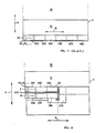
- the attached arrangement of the fusible links on a highly integrated memory chip is described with the aid of the attached FIG. 3.
- the fusible links (so-called fuses) F 1 , F 2 etc. are spatially assigned to a storage field segment 20 and arranged together with an evaluation logic 21 next to the storage field segment 20, ie in FIG. 3 below the storage field segment 20 in the lateral direction, ie in the direction of arrow B. .
- the entire arrangement of the fusible links F 1 , F 2 etc. forms a bank 10, which in turn is divided into individual fusible link boxes 101, 102, 103, ..., 106. For example, twelve melting bridges F 1 , F 2 ,... Can be located in a box 101-106.
- the evaluation logic 21 has the function of determining whether one of the fusible links F 1 , F 2 etc. has been cut or not.
- the melting of individual melting bridges takes place with a on the area in which the bank 10 of the melting bridges located, directed laser beam.
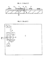
- FIGS. 1 and 2 each show in the form of a schematic cross-sectional view and a plan view of the Arrangement of small contact pads 4 on a chip 1 and such additional larger contact pads 3, 5 and 6 through an insulation layer 2 separated from the chip 1 and by additional Conductor tracks 7, 8, 9 with the original contact pads 4 are connected.
- this contacting which is the larger contact pads makes it necessary to be used before the in a melting bridge indicated with 10 bank were severed on the chip 1, can by the additional required interconnects the underlying melt bridge banks 10 are covered so that a cut all Melting bridges are no longer possible.
- FIG. 2 shows two conductor tracks 7 and 9 by way of example, which cover a fusible link bank 10. This has under another consequence that defective memory cells for chip 1 can no longer be replaced by redundant ones. Depending on Geometry of the wiring are different sized areas the melting bridges covered.
- the object is achieved by dividing the Melting bridge banks in small units and a rearrangement of the units mentioned solved in such a way that the overlying ones Wiring no longer covers the fusible links, see above that cutting the fusible links just like without that Presence of additional wiring is enabled.
- the units are like this grouped that the original width of the fusible link is halved and that both halves of the fusible link bank in a direction perpendicular to the width direction side by side lie.
- the melting bridges are at one end where they cross Adjacent to the width direction with a ground path connected and with their opposite other ends each individually wired with the associated evaluation logic.
- the melting bridges are wired to the evaluation logic e.g. B. in a single level of the chip.
- This wiring can also be used in several wiring levels instead be led to the area increase resulting from this Wiring means to keep it as small as possible.
- one becomes the conductor tracks for contacting of the additional large contact pads try to guide that halving the width of the fusible link bank or -benches sufficient to ensure that all fusible links the bank or banks are accessible and the additional Space requirements through the new wiring of the melting bridges to keep it as small as possible.
- the melting bridge arrangement proposed according to the invention can for both column and row melting bridges as well as for any other type of fusible link, e.g. B. for trimming internal voltages.
- the melting bridges F 1 , F 2 ,... Belonging to a bank 10 are divided into boxes 101, 102, 103, 104, 105, 106 and these are grouped together in two halves I and II in the direction of arrow A.
- One side of the fusible links F 1 , F 2 , ... is connected to a ground line 110 and the other side is wired to the evaluation logic 21 by conductor tracks 112.
- This wiring 112 can be routed in one or more wiring levels in order to keep the area increase that results from this wiring as small as possible.
- An example of the area increase of a wiring 112 when it is routed in one plane of the chip results as follows: 14 ⁇ m height of the fusible link boxes 101, 102, 103, ... (in the direction of arrow A) + 18 ⁇ m for the additional wiring 112 when guiding in a metal plane with a cell field pitch of 0.5 ⁇ m over the entire chip length x 2, since there are two rows I and II of rows of fusible link banks in the spine; this results in 0.5 mm 2 and corresponds to 1.6% of the total chip area of an assumed 64 M memory chip.
- the entire position of the bank 10 can be maintained the position of the evaluation logic 21 are shifted. This can but too much space for wiring pull yourself.
Landscapes
- Design And Manufacture Of Integrated Circuits (AREA)
- Semiconductor Memories (AREA)
Abstract
Description
- Die Figuren 1 und 2
- jeweils in schematischem Querschnitt und in einer Draufsicht die bereits beschriebene Anordnung von Kontaktpads und Leiterbahnen über einer Schmelzbrückenbank.
- Figur 3
- eine schematische Draufsicht auf einen Abschnitt eines Speicherchips mit einem Speicherfeldsegment.
- Figur 4
- eine Draufsicht auf einen Abschnitt eines Speicherchips mit einem Ausführungsbeispiel einer erfindungsgemäßen Schmelzbrückenanordnung.
Claims (5)
- Schmelzbrückenanordnung in oder auf integrierten Schaltungen, insbesondere hochintegrierten Speicherchips, bei denen jeweils eine Bank (10) von Schmelzbrücken (F1, F2, ...) zusammen mit einer mit den Schmelzbrücken (F1, F2, ...) elektrisch verbunden Auswertelogik (21), die feststellt, ob eine oder mehrere der Schmelzbrücken (F1, F2, ...) durchtrennt ist, neben und in Zuordnung zu einem Speicherfeldsegment (20) angeordnet ist,
dadurch gekennzeichnet, dass
eine oder mehrere in kleinere Einheiten (101, ...106) aufgeteilte Bänke (10) der Schmelzbrücken (F1, F2, ...) unter Einschränkung der Breite(n) (B) der Bank (10) bzw. Bänke so gruppiert sind, dass wenigstens ein Teil der Schmelzbrücken (F1, F2, ...) quer zur Breitenrichtung der Bank (10) nebeneinander liegt. - Schmelzbrückenanordnung nach Anspruch 1,
dadurch gekennzeichnet, dass
die ursprüngliche Breite der Schmelzbrückenbank halbiert ist, und beide Hälften (I, II) senkrecht zur Breitenrichtung (B) der Bank (10) nebeneinander liegen. - Schmelzbrückenanordnung nach Anspruch 1 oder 2,
dadurch gekennzeichnet, dass
die Schmelzbrücken (F1, F2...) an ihrem einen Ende, wo sie quer zur Breitenrichtung (B) aneinandergrenzen, mit einer Massebahn (110) verbunden sind und mit ihren entgegengesetzten anderen Enden jeweils einzeln mit der zugehörigen Auswertelogik (21) verdrahtet sind. - Schmelzbrückenanordnung nach Anspruch 3,
dadurch gekennzeichnet, dass
die Verdrahtung (112) der Schmelzbrücken (F1, F2, ...) mit der Auswertelogik (21) in einer oder mehreren Metallisierungsebenen des Chips (1) geführt ist. - Hochintegrierter Speicherchip
gekennzeichnet durch
die Anwendung der Schmelzbrückenanordnung nach einem der Ansprüche 1 bis 4.
Applications Claiming Priority (2)
| Application Number | Priority Date | Filing Date | Title |
|---|---|---|---|
| DE10006243 | 2000-02-11 | ||
| DE10006243A DE10006243A1 (de) | 2000-02-11 | 2000-02-11 | Schmelzbrückenanordnung in integrierten Schaltungen |
Publications (3)
| Publication Number | Publication Date |
|---|---|
| EP1139423A2 true EP1139423A2 (de) | 2001-10-04 |
| EP1139423A3 EP1139423A3 (de) | 2004-07-28 |
| EP1139423B1 EP1139423B1 (de) | 2006-05-10 |
Family
ID=7630681
Family Applications (1)
| Application Number | Title | Priority Date | Filing Date |
|---|---|---|---|
| EP01101997A Expired - Lifetime EP1139423B1 (de) | 2000-02-11 | 2001-01-29 | Schmelzbrückenanordnung in integrierten Schaltungen |
Country Status (4)
| Country | Link |
|---|---|
| US (1) | US6407586B2 (de) |
| EP (1) | EP1139423B1 (de) |
| DE (2) | DE10006243A1 (de) |
| TW (1) | TW492174B (de) |
Families Citing this family (1)
| Publication number | Priority date | Publication date | Assignee | Title |
|---|---|---|---|---|
| DE10231206B4 (de) * | 2002-07-10 | 2014-10-30 | Qimonda Ag | Halbleitervorrichtung |
Family Cites Families (10)
| Publication number | Priority date | Publication date | Assignee | Title |
|---|---|---|---|---|
| US4910418A (en) * | 1988-12-29 | 1990-03-20 | Gazelle Microcircuits, Inc. | Semiconductor fuse programmable array structure |
| EP0706172A1 (de) | 1994-10-04 | 1996-04-10 | Hughes Aircraft Company | Sprachkodierer und Dekodierer mit niedriger Bitrate |
| US5495181A (en) * | 1994-12-01 | 1996-02-27 | Quicklogic Corporation | Integrated circuit facilitating simultaneous programming of multiple antifuses |
| TW279229B (en) * | 1994-12-29 | 1996-06-21 | Siemens Ag | Double density fuse bank for the laser break-link programming of an integrated-circuit |
| US5532966A (en) * | 1995-06-13 | 1996-07-02 | Alliance Semiconductor Corporation | Random access memory redundancy circuit employing fusible links |
| US5905295A (en) * | 1997-04-01 | 1999-05-18 | Micron Technology, Inc. | Reduced pitch laser redundancy fuse bank structure |
| US5859801A (en) * | 1997-03-28 | 1999-01-12 | Siemens Aktiengesellschaft | Flexible fuse placement in redundant semiconductor memory |
| US5835425A (en) * | 1997-09-04 | 1998-11-10 | Siemens Aktiengesellschaft | Dimension programmable fusebanks and methods for making the same |
| JPH11154706A (ja) * | 1997-11-20 | 1999-06-08 | Mitsubishi Electric Corp | 半導体装置 |
| JP2000100195A (ja) * | 1998-09-22 | 2000-04-07 | Nec Corp | 冗長回路を有する半導体記憶装置 |
-
2000
- 2000-02-11 DE DE10006243A patent/DE10006243A1/de not_active Withdrawn
-
2001
- 2001-01-29 EP EP01101997A patent/EP1139423B1/de not_active Expired - Lifetime
- 2001-01-29 DE DE50109730T patent/DE50109730D1/de not_active Expired - Lifetime
- 2001-02-09 TW TW090102889A patent/TW492174B/zh not_active IP Right Cessation
- 2001-02-12 US US09/781,813 patent/US6407586B2/en not_active Expired - Lifetime
Also Published As
| Publication number | Publication date |
|---|---|
| DE50109730D1 (de) | 2006-06-14 |
| DE10006243A1 (de) | 2001-08-23 |
| US20010019167A1 (en) | 2001-09-06 |
| EP1139423A3 (de) | 2004-07-28 |
| TW492174B (en) | 2002-06-21 |
| US6407586B2 (en) | 2002-06-18 |
| EP1139423B1 (de) | 2006-05-10 |
Similar Documents
| Publication | Publication Date | Title |
|---|---|---|
| DE69526006T2 (de) | Anordnung mit einem einzigen Verdrillungsgebiet und Verfahren für gepaarte linienförmige Leiter in integrierten Schaltungen | |
| DE60011190T2 (de) | Gemischte Sicherungstechnologien | |
| DE19619737C2 (de) | Halbleitereinrichtung mit einer Ersatzschaltung und einer Sicherungsschicht und Verfahren zur Herstellung einer derartigen Halbleitereinrichtung | |
| DE2633079A1 (de) | Anordnung zum verbinden bzw. integrieren einer vielzahl von getrennten speichern auf einem scheibchen | |
| DE69325133T2 (de) | Halbleiterfestwertspeicher | |
| DE102020111649A1 (de) | Integrierte Schaltungsvorrichtung | |
| DE19507127A1 (de) | Adaptersystem für Baugruppen-Platinen, zu verwenden in einer Prüfeinrichtung | |
| DE2418906B2 (de) | Verfahren zur Verbindung der in einer Halbleiterscheibe erzeugten Schaltungskreise | |
| EP1368833B1 (de) | Integrierte schaltung mit elektrischen verbindungselementen | |
| DE10044148A1 (de) | Elektronisches Bauteil mit gestapelten Bausteinen und Verfahren zu seiner Herstellung | |
| DE10306949A1 (de) | Halbleitereinrichtung | |
| EP1139423B1 (de) | Schmelzbrückenanordnung in integrierten Schaltungen | |
| DE10126610A1 (de) | Halbleiterchip, Speichermodul und Verfahren zum Testen des Halbleiterchips | |
| DE10231206B4 (de) | Halbleitervorrichtung | |
| DE102004060369A1 (de) | Halbleiterscheibe mit Teststruktur | |
| DE19908428C2 (de) | Halbleiterspeicheranordnung mit Bitleitungs-Twist | |
| DE4132849A1 (de) | Verfahren zur automatischen verdrahtung in einer halbleiterschaltungsanordnung | |
| DE602004000651T2 (de) | Integrierte Spannungsreglerschaltung und deren Herstellungsverfahren | |
| DE2425915B2 (de) | Verfahren zum herstellen von integrierten halbleiterschaltungen | |
| DE60116774T2 (de) | Leiterbahnen innerhalb eines belichtungsfensters für laser-schmelzsicherungen | |
| DE19631133A1 (de) | Halbleitervorrichtung mit einer Sicherungsschicht | |
| DE60118833T2 (de) | Halbleiter-Speicher mit unterteilter Wortleitungstruktur | |
| DE68917793T2 (de) | Integrierte Vorrichtung in Halbleiterscheibengrösse. | |
| DE10054447A1 (de) | Halbleiterspeicherbauelement mit Zellenversorgungs-Reparaturschaltkreisen und Verfahren zum Anordnen derselben | |
| DE202021106814U1 (de) | Schaltungsstruktur für die Erkennung und Umgehung von Unterbrechungen und Kurzschlüssen in einer PCB-basierten Spule |
Legal Events
| Date | Code | Title | Description |
|---|---|---|---|
| PUAI | Public reference made under article 153(3) epc to a published international application that has entered the european phase |
Free format text: ORIGINAL CODE: 0009012 |
|
| AK | Designated contracting states |
Kind code of ref document: A2 Designated state(s): AT BE CH CY DE DK ES FI FR GB GR IE IT LI LU MC NL PT SE TR |
|
| AX | Request for extension of the european patent |
Free format text: AL;LT;LV;MK;RO;SI |
|
| PUAL | Search report despatched |
Free format text: ORIGINAL CODE: 0009013 |
|
| AK | Designated contracting states |
Kind code of ref document: A3 Designated state(s): AT BE CH CY DE DK ES FI FR GB GR IE IT LI LU MC NL PT SE TR |
|
| AX | Request for extension of the european patent |
Extension state: AL LT LV MK RO SI |
|
| 17P | Request for examination filed |
Effective date: 20050128 |
|
| AKX | Designation fees paid |
Designated state(s): DE FR GB IE IT |
|
| 17Q | First examination report despatched |
Effective date: 20050311 |
|
| GRAP | Despatch of communication of intention to grant a patent |
Free format text: ORIGINAL CODE: EPIDOSNIGR1 |
|
| GRAS | Grant fee paid |
Free format text: ORIGINAL CODE: EPIDOSNIGR3 |
|
| GRAA | (expected) grant |
Free format text: ORIGINAL CODE: 0009210 |
|
| AK | Designated contracting states |
Kind code of ref document: B1 Designated state(s): DE FR GB IE IT |
|
| PG25 | Lapsed in a contracting state [announced via postgrant information from national office to epo] |
Ref country code: IT Free format text: LAPSE BECAUSE OF FAILURE TO SUBMIT A TRANSLATION OF THE DESCRIPTION OR TO PAY THE FEE WITHIN THE PRESCRIBED TIME-LIMIT;WARNING: LAPSES OF ITALIAN PATENTS WITH EFFECTIVE DATE BEFORE 2007 MAY HAVE OCCURRED AT ANY TIME BEFORE 2007. THE CORRECT EFFECTIVE DATE MAY BE DIFFERENT FROM THE ONE RECORDED. Effective date: 20060510 |
|
| REG | Reference to a national code |
Ref country code: GB Ref legal event code: FG4D Free format text: NOT ENGLISH |
|
| REF | Corresponds to: |
Ref document number: 50109730 Country of ref document: DE Date of ref document: 20060614 Kind code of ref document: P |
|
| REG | Reference to a national code |
Ref country code: IE Ref legal event code: FG4D Free format text: LANGUAGE OF EP DOCUMENT: GERMAN |
|
| GBT | Gb: translation of ep patent filed (gb section 77(6)(a)/1977) |
Effective date: 20060809 |
|
| PLBE | No opposition filed within time limit |
Free format text: ORIGINAL CODE: 0009261 |
|
| STAA | Information on the status of an ep patent application or granted ep patent |
Free format text: STATUS: NO OPPOSITION FILED WITHIN TIME LIMIT |
|
| 26N | No opposition filed |
Effective date: 20070213 |
|
| EN | Fr: translation not filed | ||
| PG25 | Lapsed in a contracting state [announced via postgrant information from national office to epo] |
Ref country code: FR Free format text: LAPSE BECAUSE OF FAILURE TO SUBMIT A TRANSLATION OF THE DESCRIPTION OR TO PAY THE FEE WITHIN THE PRESCRIBED TIME-LIMIT Effective date: 20070309 |
|
| PG25 | Lapsed in a contracting state [announced via postgrant information from national office to epo] |
Ref country code: FR Free format text: LAPSE BECAUSE OF FAILURE TO SUBMIT A TRANSLATION OF THE DESCRIPTION OR TO PAY THE FEE WITHIN THE PRESCRIBED TIME-LIMIT Effective date: 20060510 |
|
| REG | Reference to a national code |
Ref country code: GB Ref legal event code: 732E Free format text: REGISTERED BETWEEN 20100916 AND 20100922 |
|
| REG | Reference to a national code |
Ref country code: GB Ref legal event code: 732E Free format text: REGISTERED BETWEEN 20110804 AND 20110810 |
|
| REG | Reference to a national code |
Ref country code: DE Ref legal event code: R081 Ref document number: 50109730 Country of ref document: DE Owner name: INFINEON TECHNOLOGIES AG, DE Free format text: FORMER OWNER: QIMONDA AG, 81739 MUENCHEN, DE Ref country code: DE Ref legal event code: R081 Ref document number: 50109730 Country of ref document: DE Owner name: POLARIS INNOVATIONS LTD., IE Free format text: FORMER OWNER: QIMONDA AG, 81739 MUENCHEN, DE |
|
| REG | Reference to a national code |
Ref country code: DE Ref legal event code: R081 Ref document number: 50109730 Country of ref document: DE Owner name: POLARIS INNOVATIONS LTD., IE Free format text: FORMER OWNER: INFINEON TECHNOLOGIES AG, 85579 NEUBIBERG, DE |
|
| REG | Reference to a national code |
Ref country code: GB Ref legal event code: 732E Free format text: REGISTERED BETWEEN 20151015 AND 20151021 |
|
| REG | Reference to a national code |
Ref country code: GB Ref legal event code: 732E Free format text: REGISTERED BETWEEN 20160310 AND 20160316 |
|
| PGFP | Annual fee paid to national office [announced via postgrant information from national office to epo] |
Ref country code: GB Payment date: 20170125 Year of fee payment: 17 Ref country code: IE Payment date: 20170109 Year of fee payment: 17 |
|
| PGFP | Annual fee paid to national office [announced via postgrant information from national office to epo] |
Ref country code: DE Payment date: 20180117 Year of fee payment: 18 |
|
| GBPC | Gb: european patent ceased through non-payment of renewal fee |
Effective date: 20180129 |
|
| REG | Reference to a national code |
Ref country code: IE Ref legal event code: MM4A |
|
| PG25 | Lapsed in a contracting state [announced via postgrant information from national office to epo] |
Ref country code: GB Free format text: LAPSE BECAUSE OF NON-PAYMENT OF DUE FEES Effective date: 20180129 |
|
| PG25 | Lapsed in a contracting state [announced via postgrant information from national office to epo] |
Ref country code: IE Free format text: LAPSE BECAUSE OF NON-PAYMENT OF DUE FEES Effective date: 20180129 |
|
| REG | Reference to a national code |
Ref country code: DE Ref legal event code: R119 Ref document number: 50109730 Country of ref document: DE |
|
| PG25 | Lapsed in a contracting state [announced via postgrant information from national office to epo] |
Ref country code: DE Free format text: LAPSE BECAUSE OF NON-PAYMENT OF DUE FEES Effective date: 20190801 |