EP1136864A2 - Optisches Modul - Google Patents
Optisches Modul Download PDFInfo
- Publication number
- EP1136864A2 EP1136864A2 EP01107206A EP01107206A EP1136864A2 EP 1136864 A2 EP1136864 A2 EP 1136864A2 EP 01107206 A EP01107206 A EP 01107206A EP 01107206 A EP01107206 A EP 01107206A EP 1136864 A2 EP1136864 A2 EP 1136864A2
- Authority
- EP
- European Patent Office
- Prior art keywords
- optical
- resin
- inner container
- substrate
- container
- Prior art date
- Legal status (The legal status is an assumption and is not a legal conclusion. Google has not performed a legal analysis and makes no representation as to the accuracy of the status listed.)
- Withdrawn
Links
Images


Classifications
-
- G—PHYSICS
- G02—OPTICS
- G02B—OPTICAL ELEMENTS, SYSTEMS OR APPARATUS
- G02B6/00—Light guides; Structural details of arrangements comprising light guides and other optical elements, e.g. couplings
- G02B6/24—Coupling light guides
- G02B6/42—Coupling light guides with opto-electronic elements
- G02B6/4201—Packages, e.g. shape, construction, internal or external details
- G02B6/4219—Mechanical fixtures for holding or positioning the elements relative to each other in the couplings; Alignment methods for the elements, e.g. measuring or observing methods especially used therefor
- G02B6/4236—Fixing or mounting methods of the aligned elements
- G02B6/4239—Adhesive bonding; Encapsulation with polymer material
-
- G—PHYSICS
- G02—OPTICS
- G02B—OPTICAL ELEMENTS, SYSTEMS OR APPARATUS
- G02B6/00—Light guides; Structural details of arrangements comprising light guides and other optical elements, e.g. couplings
- G02B6/24—Coupling light guides
- G02B6/42—Coupling light guides with opto-electronic elements
- G02B6/4201—Packages, e.g. shape, construction, internal or external details
- G02B6/4251—Sealed packages
- G02B6/4253—Sealed packages by embedding housing components in an adhesive or a polymer material
-
- G—PHYSICS
- G02—OPTICS
- G02B—OPTICAL ELEMENTS, SYSTEMS OR APPARATUS
- G02B6/00—Light guides; Structural details of arrangements comprising light guides and other optical elements, e.g. couplings
- G02B6/24—Coupling light guides
- G02B6/42—Coupling light guides with opto-electronic elements
- G02B6/4201—Packages, e.g. shape, construction, internal or external details
- G02B6/4256—Details of housings
- G02B6/4257—Details of housings having a supporting carrier or a mounting substrate or a mounting plate
-
- G—PHYSICS
- G02—OPTICS
- G02B—OPTICAL ELEMENTS, SYSTEMS OR APPARATUS
- G02B6/00—Light guides; Structural details of arrangements comprising light guides and other optical elements, e.g. couplings
- G02B6/24—Coupling light guides
- G02B6/26—Optical coupling means
- G02B6/30—Optical coupling means for use between fibre and thin-film device
-
- G—PHYSICS
- G02—OPTICS
- G02B—OPTICAL ELEMENTS, SYSTEMS OR APPARATUS
- G02B6/00—Light guides; Structural details of arrangements comprising light guides and other optical elements, e.g. couplings
- G02B6/24—Coupling light guides
- G02B6/42—Coupling light guides with opto-electronic elements
- G02B6/4201—Packages, e.g. shape, construction, internal or external details
- G02B6/4204—Packages, e.g. shape, construction, internal or external details the coupling comprising intermediate optical elements, e.g. lenses, holograms
- G02B6/4212—Packages, e.g. shape, construction, internal or external details the coupling comprising intermediate optical elements, e.g. lenses, holograms the intermediate optical element being a coupling medium interposed therebetween, e.g. epoxy resin, refractive index matching material, index grease, matching liquid or gel
-
- G—PHYSICS
- G02—OPTICS
- G02B—OPTICAL ELEMENTS, SYSTEMS OR APPARATUS
- G02B6/00—Light guides; Structural details of arrangements comprising light guides and other optical elements, e.g. couplings
- G02B6/24—Coupling light guides
- G02B6/42—Coupling light guides with opto-electronic elements
- G02B6/4201—Packages, e.g. shape, construction, internal or external details
- G02B6/4219—Mechanical fixtures for holding or positioning the elements relative to each other in the couplings; Alignment methods for the elements, e.g. measuring or observing methods especially used therefor
- G02B6/4236—Fixing or mounting methods of the aligned elements
- G02B6/424—Mounting of the optical light guide
- G02B6/4243—Mounting of the optical light guide into a groove
-
- G—PHYSICS
- G02—OPTICS
- G02B—OPTICAL ELEMENTS, SYSTEMS OR APPARATUS
- G02B6/00—Light guides; Structural details of arrangements comprising light guides and other optical elements, e.g. couplings
- G02B6/24—Coupling light guides
- G02B6/42—Coupling light guides with opto-electronic elements
- G02B6/4201—Packages, e.g. shape, construction, internal or external details
- G02B6/4256—Details of housings
- G02B6/4262—Details of housings characterised by the shape of the housing
- G02B6/4265—Details of housings characterised by the shape of the housing of the Butterfly or dual inline package [DIP] type
-
- H—ELECTRICITY
- H10—SEMICONDUCTOR DEVICES; ELECTRIC SOLID-STATE DEVICES NOT OTHERWISE PROVIDED FOR
- H10W—GENERIC PACKAGES, INTERCONNECTIONS, CONNECTORS OR OTHER CONSTRUCTIONAL DETAILS OF DEVICES COVERED BY CLASS H10
- H10W72/00—Interconnections or connectors in packages
- H10W72/50—Bond wires
- H10W72/551—Materials of bond wires
- H10W72/552—Materials of bond wires comprising metals or metalloids, e.g. silver
- H10W72/5522—Materials of bond wires comprising metals or metalloids, e.g. silver comprising gold [Au]
Definitions
- the present invention relates to an optical module used for optical communications, for example, an optical module such as an optical transmitter, an optical receiver, an optical demultiplexer, or an optical multiplexer.
- an optical module such as an optical transmitter, an optical receiver, an optical demultiplexer, or an optical multiplexer.
- it relates to the improvement of a package structure and a portion where optical fibers are fixed.
- optical coupling between an optical fiber and an optical device such as a photo diode (PD) and a laser diode (LD) was often achieved via a free space by using a lens.
- a lens is used for focusing light.
- the light exits once in the free space it is effective to provide the lens.
- problems such as the difference in thermal expansion coefficient between the optical fiber and element, stress, and distortion do not occur.
- a prior-art example will be described with reference to the optical transmitter and the receiver.
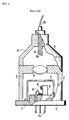
- FIG. 1 is a longitudinal section showing an example of the transmitter which is most commonly adopted for practical use.
- An outer fence comprises a metallic circular stem 1, a cylindrical metallic lens holder 2, and a metallic conic ferrule holder 3.
- the housing has a shape with an axial-symmetric three-dimensional expanse.
- a pole 4 is provided on the upper surface of the stem 1 and on the side thereof, an LD 5 is fixed.
- the LD has its end faces directed in the vertical direction so that light is emitted in the axial direction.
- An upper surface-illuminated type monitor PD 6 is fixed on the central part of the stem 1.
- a cylindrical cap 7 is attached so that the LD 5 and the PD 6 are surrounded.
- a lens holder 2 is fixed so that the cap is surrounded.
- a lens 8 is positioned directly above the LD 5.
- a tubular ferrule 9 grasps the tip end of an optical fiber 10.
- the ferrule 9 is inserted in a hole on the top portion of the ferrule holder 3.
- the axis of the optical fiber 10 exists on the center line of a metallic package (the stem 1, lens holder 2, and ferrule holder 3). That is, the center of the stem 1, the PD 6, the LD 5, the lens 8, and the optical fiber 10 are lined on the center line.
- the lens holder 2 and the ferrule holder 3 each having a three-dimensional structure are aligned with respect to the x-y surface and the ferrule 9 is aligned in the z direction, and they are then fixed.
- lead pins 11 are terminal ends to connect to an external electric circuit.
- a PD module having a similar three-dimensional structure is also used.
- illustration thereof is omitted.
- a beam of light is perpendicular to the stem surface and the optical fiber protrudes from the top portion of the package. The ray of light exits from the optical fiber to the free space and enters the optical element, or it exits from the optical element and enters the optical fiber via the free space.
- the module having such a three-dimensional structure covered by the metal package is advantageous in that it can shut out external noise, has a long life without being affected by moisture and oxygen in the open air, and also has high reliability.
- the present structures of the LD module shown in FIG. 1 and the PD module are excellent. However, there is a considerable number of components, alignment thereof takes much time and labor, and the production cost is high. In addition, they have the drawback of having a large shape. The shape and structure without change has limited cost reduction.
- a structure of a module wherein an optical fiber is fixed parallel to a bench surface so that a beam of light is parallel with a substrate surface (package surface) is generally referred to as the surface-mount type.
- various types are included.
- a free space air, vacuum
- the space between an optical fiber and an optical device is covered by a resin.
- the present invention relates to a module wherein the section between the optical fiber and devices is covered by a resin.
- the object of the present invention is to provide a module that the section between the optical fiber and devices is covered by a resin. Now, a prior art wherein such a section is covered by a resin will be described.
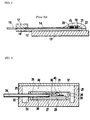
- a structure as in FIG. 2 has been studied.
- a horizontal Si substrate 12 is mounted on a horizontal package terrace 13.
- a Planar Lightwave Circuit (PLC) layer 14 is formed on the Si substrate 12.
- This comprises an SiO 2 layer formed thereon by oxidizing the Si substrate or an SiO 2 layer by sputtering.
- PLC Planar Lightwave Circuit
- a part with a high refractive index is linearly formed and it serves as a light guide (waveguide).
- an LD 15 is fixed on an extension of the waveguide (axis).
- a PD 16 for monitoring is mounted. This serves to monitor LD power and to maintain the LD power stably.
- a fixing portion 17 is provided at the front end of the waveguide, and in a hole 18 thereof, the tip end of an optical fiber 19 is inserted and fixed.
- the optical fiber 19, the waveguide, the LD 15, and the PD 16 are lined up straight on the substrate surface.
- Light which is emitted from the LD propagates in parallel with the surface of the substrate. Therefore, the structure is referred to as the surface-mount type.
- a transparent silicone resin 21 covers the terminal end 20 of the waveguide, the LD 15, and the PD 16.
- the light which is emitted forward from the LD 15 propagates through the transparent resin 21 and enters the waveguide terminal end 20.
- the light which is emitted rearward from LD 15 propagates through the transparent resin 21 and enters the PD 16.
- the light from the LD propagates only through the resin without going out to the free space. Naturally, the resin must be transparent since the light passes therethrough.
- the transparent resin 21 lacks moisture resistance and stress resistance, the outside thereof is covered by a black epoxy resin 22. Since the epoxy resin becomes a hard and solid coating when being hardened, the epoxy resin is excellent in airtightness, mechanical strength, and moisture resistance, etc. Thus, by double-sealing the PD and LD by means of two types of resins with different properties, necessary characteristics such as moisture resistance, stress resistance, and strength are realized, while allowing light to pass therethrough.
- FIG. 2 The prior-art example of FIG. 2 has been suggested, for example, in 1 ⁇ "Highly reliable resin-sealed LD-PD module" by Fumio Ichikawa, Mitsuo Fukuda, Yasufumi Yamada, Kuniharu Kato, Koji Sato, and Hiroshi Toba, in the General Convention of the Electronic Society of 1998, C-3-161, p.327.
- a silicone resin which is transparent and flexible is used for portions through which light needs to pass such as the PD, LD, and the end of the waveguide.
- the outside thereof is covered by a strong epoxy resin, whereby environment resistance is enhanced.
- the module is lower in price than a metal package. Because of the surface-mount type, the time and labor for alignment is unnecessary. Since the structure does not have a three-dimensional structure but has a two dimensional structure, a smaller size can be achieved.
- This structure is characterized by double-sealing by means of resins.
- An inside transmittance (transparent resin) and an outside opaque resin are complementarily utilized.
- a transparent resin is used on the inside in order to suppress the reflection of light on the boundary between the waveguide and space.
- a silicone-based resin is used.
- the transparent resin not only transmits light but also reduces reflection on the end face, whereby the light is suppressed from spreading.
- the inside transparent resin does not harden into a solid but is in a gel form and is flexible, that is, a soft resin. Since the resin covers the LD and PD, it also serves to protect these semiconductor chips from the outside area.
- the transparent resin has flexibility and also has an effect to protect a wire for conduction. If the wire is covered over by a hard resin, the wire can be broken due to shocks, etc., however, since the wire is covered by the flexible resin, it is prevented from being cut.
- the transparent resin itself is soft, it does not cause damage or distortion to the chips and the optical fiber. Such a characteristic of softness is advantageous in the mechanical aspect.
- the transparent silicone resin has drawbacks. It has high permeability and lacks moisture resistance. The fact that it is flexible means, on the other hand, that a fixed shape cannot be obtained.
- Such a resin as this is entirely covered by an epoxy-based resin in order to fix the shape and improve the moisture resistance.
- the epoxy-based resin is excellent in hardening ability and fixes its shape. It is excellent in shapeability. It is also excellent in moisture resistance and high in reliability.
- the epoxy-based resin does not have transmittance and is suitable to prevent light from entering from the outside area.
- Such a double sealing resin structure as 1 ⁇ has the abovedescribed advantages.
- this double sealing structure has some disadvantages.
- a silicone-based resin is coated on the end of a waveguide and narrow portions between the LD and PD, then is hardened by means of heat and ultraviolet ray, etc. It is preferable if the resin forms a round shape due to surface tension and stops in a condition where about only the area of the PD, LD, and the end of the waveguide are covered.
- This resin is high in fluidity and it does not easily stick to and fit to the substrate. Therefore, the resin slips and flows about the horizontal surface of the substrate.
- the silicon-based resin does not stay at a fixed point and flows due to vibration, inclination, the direction where the resin drops, and instability in supplying pressure. There is also a case where it flows excessively, coats widely, and solidifies on the substrate.
- the resin Since the resin is used to enhance smoothness, even if an epoxy resin is coated thereon, the epoxy resin is repelled and flows. That is, an excessive amount of silicone-based resin hinders adhesion of the epoxy resin. If the substrate surface is exposed, the epoxy resin can be adhered, however, if the substrate surface is broadly covered by the silicone based resin, the epoxy resin does not fit. Then, since it cannot be closely fitted to the substrate, the resin comes off. In addition, if it broadens to a lead frame, it covers the upper surface of the lead frame. In this case, wire bonding becomes impossible, and wiring cannot be performed.
- the device of FIG. 2 has the resin-double covering structure, however, since there is nothing to restrict the silicone-based resin as the base to flow, the abovementioned disadvantages exist.
- a first object of the present invention is to provide a package structure wherein fluidity of a silicone resin as the base is restricted so that a silicone-based resin does not widely cover a substrate.
- a second object of the present invention is to provide a package structure wherein a silicone-based resin is prevented from flowing into an unnecessary part, whereby a strong covering of an epoxy resin becomes possible.
- a package structure of a module of the present invention comprises an inner barrier structure to store a soft silicone-based resin in a gel form and an outer shell structure composed of a fixing resin which surrounds the outside of the inner barrier structure. That is, an inner container for a silicone-based resin is provided inside the package. Therefore, a container having an inside-and-outside double structure is provided comprising the inner container having the barrier inside thereof and the outer container.
- the inner container and outer container can be formed of the same package material. Otherwise, the outer fence portion on the outside may be formed not of the package material but by hardening an epoxy resin.
- An optical fiber end and optical devices such as an LD, and a PD, etc. are provided in the inner container and they are filled with a silicone-based resin. Thereon, an epoxy resin is poured to fill the outer container of the package and solidified.
- the package has the double structure as well as the resins do.
- a transparent silicone-based resin is filled inside the inner container.
- This base resin completely covers the optical devices and optical fiber end. It also covers the wire.
- the inner container is surrounded by walls, the resin having fluidity does not overflow. The resin does not flow freely on the substrate. The resin does not moisten broadly on the substrate to hinder the epoxy resin from fitting. The effect of the barriers of the inner container is the most advantageous in terms of holding the transparent resin (inner resin) without being spilled.
- the inner resin (transparent resin, silicone-based) 35 is transparent and guides light to the section between optical fibers or between an optical fiber and an optical element.
- the refractive index of the resin is almost the same as that of the optical fiber so that reflection on the end face is minimal and the light does not spread.
- the inner resin also acts to protect the wire from being applied with a stress.
- the outer resin (fixation resin such as an epoxy) 36 hardens, whereby it protects the inner structure. Since the outer resin does not serve to guide light, it can be black. It also has an airtight-sealing function to prevent water from entering by trickling down a lead frame.
- the present invention provides a package having a structure of a plane-mount type and an inside-and-outside double structure comprising an inner container having a barrier and a hard outer container, wherein a glue that is high in fluidity can be stored in the inner container.
- the range where a silicone-based resin spreads can be limited in the production process with accuracy.
- the inner container is especially novel and it brings about a benefit in the production process.
- the outer container provides mechanical strength and airtightness. When a silicone-based transparent resin sticks to a package surface, it repels an epoxy resin and reduces the adhesion, however, the silicone-based resin does not flow out in the present invention. Therefore, a fixing resin of the epoxy base, etc. can form a firm outer shell portion at all times.
- the present invention provides a double resin structure comprising flexible and rigid resins which is skillfully combined and it has a complementary effect. Since the inside is made of a transparent resin, light transmission between an optical fiber and an optical element are not spoiled. Since the resin is in a gel form, it reduces stress, the stress is not applied on the optical element, and a wire is prevented from being cut. These are the effects of a completed transparent resin product. Furthermore, since a hard resin is used on the outside, the strength for fixing an optical fiber is high. The structure is airtight and has excellent moisture resistance. The circumference of the lead frame can be fixed by the epoxy resin, whereby the strength and moisture resistance can be improved.
- the package structure is made of the resins, mass production is possible and the optical devices and optical fiber can easily be mounted at low cost. According to the present invention, reduction in cost and size of a wide range of optical modules can stably be realized. Thus, the spread of optical transmission to each home is more actively enhanced.
- FIG. 1 is a section of an LD module according to the prior art which is accommodated in a metal package and has a three-dimensional structure.
- FIG. 2 is a longitudinal section of an LD module of a surface-mount type according to the prior art, wherein an optical waveguide layer is provided on the plane substrate, LD and PD chips are attached at the terminal ends of the optical waveguides, and the LD, PD, and the ends of optical waveguides are covered by a transparent resin, and an epoxy resin covers thereon.
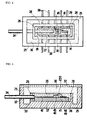
- FIG. 3 is a longitudinal section showing Example 1 having a double barrier structure and double glue structure, wherein the present invention is applied to a transmitter.
- FIG. 4 is a plane view showing Example 1 having a double barrier structure and double glue structure, wherein the present invention is applied to a transmitter.
- FIG. 5 is a longitudinal section showing Example 3 having a double barrier structure and double glue structure, wherein the present invention is applied to a transmitting and receiving device.
- FIG. 6 is a longitudinal section showing only the substrate of Example 3 having a double barrier structure and double glue structure, wherein the present invention is applied to a transmitter.
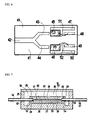
- FIG. 7 is a longitudinal section showing Example 4 having a double barrier structure and double glue structure, wherein the present invention is applied to an optical multiplexer and an optical demultiplexer.
- FIG. 8 is a longitudinal section showing only the substrate of Example 4 having a double barrier structure and double glue structure, wherein the present invention is applied to an optical multiplexer and an optical demultiplexer.
- FIG. 9 is a longitudinal section showing Example 5, wherein the present invention is applied to an LD and PD module with a lens.
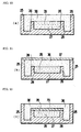
- FIG. 10 is a longitudinal section showing an embodiment of the inside-and-outside double container according to the present invention, wherein the bottom plates are identical, sidewalls are provided, and the upper portion is opened.
- FIG. 11 is a longitudinal section showing an embodiment, according to the present invention, of the inside-and-outside double container in which the bottom plates are identical, sidewalls are provided, and the upper portion is opened, wherein a lid is provided on the outer container.
- FIG. 12 is a longitudinal section showing an embodiment, according to the present invention, of the inside-and-outside double container in which the bottom plates are identical, sidewalls are provided, and the upper portion is opened, wherein a lid is provided on the inner container.
- FIG. 13 is a longitudinal section showing an embodiment, according to the present invention, of the inside-and-outside double container in which the bottom plates are identical, the inner container has sidewalls, and the upper portion is opened, wherein the outer container has no sidewall and has an outer shell portion by hardening of a resin itself.
- FIG. 14 is a longitudinal section showing an embodiment, according to the present invention, of the double container composed of separate inside and outside containers in which the bottom plates are different, sidewalls are provided, and the upper portions are opened, wherein the bottom portion of the inner container is adhered to the bottom portion of the outer container.
- FIG. 15 is a longitudinal section showing an embodiment, according to the present invention, of the double container composed of separate inside and outside containers in which the bottom plates are different, sidewalls are provided, and the upper portion is opened, wherein the bottom portion of the inner container is stuck to the bottom portion of the outer container and a lid is provided on the outer container.
- FIG. 16 is a longitudinal section showing an embodiment, according to the present invention, of the double container composed of separate inside and outside containers in which the bottom plates are different, sidewalls are provided, and the upper portion is opened, wherein the bottom portion of the inner container is adhered to the bottom portion of the outer container and a lid is provided on the inner container.
- FIG. 17 is a longitudinal section showing an embodiment, according to the present invention, of the inside-and-outside double container in which the bottom plates are different, the inner container has sidewalls, and the upper portion is opened, wherein the outer container has no sidewall, the bottom portion of the inner container is stuck to the bottom portion of the outer container, and the outer container has an outer shell portion by hardening a resin itself.
- the present invention is characterized by comprising the inner container which has a plurality of sidewalls (barriers) and stores the transparent resin, and contains optical components and the outer container fixed to the outside of the inner container by the fixing resin.
- the inner container which has a plurality of sidewalls (barriers) and stores the transparent resin, and contains optical components and the outer container fixed to the outside of the inner container by the fixing resin.
- sidewalls are provided on all sides, however the sidewalls provided on only two sides in the direction of the lead frame are satisfactory. Even by only the two barriers, the silicone resin can be prevented from sticking to the lead frame.
- the sidewalls of any type of the inner container are wall surfaces on two parallel sides or on three sides, or, preferably, on four sides (rectangular) and the heights are approximately the same.
- an inner container 26 is provided in the outer container 25 and when the plates of the bottom surfaces (bottom wall) of the inner and outer containers are common, the plates are described as a bottom plate 27.
- the inside of the inner container 26 is filled with a transparent resin 35.
- a fixing resin 36 seals the transparent resin 35 and fills the outer container 25. If the inner container and outer container are separately provided, the bottom plate 76 of the inner container and the bottom plate 75 of the outer container are glued.
- a medium for exchanging optical signals between the outside and an optical device is an optical fiber, however, there may be a case wherein an optical device is directly connected to the outside equipment. There also may be a case of connection via an optical waveguide. There may be a case of connection between the optical fiber and the LD, connection between the optical fiber and the PD, connection between the optical fiber and the PD and LD, or connection between an optical fiber and an optical fiber.
- An LD is fixed on the substrate and an optical fiber is attached hereto. This is an optical transmitter.
- An LD and monitoring PD are fixed on the substrate and an optical fiber is attached hereto. This is an optical transmitter, as well.
- a PD is fixed on the substrate and an optical fiber is attached hereto. This is an optical receiver.
- a PD and AMP are fixed on the substrate and an optical fiber is attached hereto.
- a PD signal is amplified in the AMP. This is an optical receiver, as well.
- An LD is fixed on the substrate on which an optical waveguide is formed and an optical fiber is attached on the front end face of the substrate. This is an optical transmitter.
- An LD and monitoring PD are fixed on the substrate on which optical waveguides are formed and an optical fiber is attached on the front end face of the substrate. This is an optical transmitter, as well.
- a PD is fixed on the substrate on which an optical waveguide is formed and an optical fiber is attached on the front end face of the substrate. This is an optical receiver.
- a PD and AMP are fixed on the substrate on which an optical waveguide is formed and an optical fiber is attached on the front end face of the substrate.
- a PD signal is amplified in the AMP. This is an optical receiver, as well.
- Optical fibers are attached to the end faces of the substrate on which an optical waveguide is formed. If an optical fiber is attached to each end, a simple relay is produced. However, by providing a Y-branch in the optical waveguides and fixing optical fibers to the end face of the substrate that lead to both ends of the branch, an optical demultiplexer and an optical multiplexer can be produced.
- FIG. 3 section
- FIG. 4 plane view
- the outer container 25 whose upper portion is opened and the inner container 26 which is formed inside the outer containers have the bottom plates 27 jointly.
- the inner container 26 has barriers 28 on all sides thereof. The barriers are provided so that a fluid can be held.
- the barriers of the inner container 26 are shorter than the sidewalls of the outer container 25. Since the containers have the bottom plates 27 jointly and the upper portions of both containers are opened, the container can be shaped from plastic, etc. They can be produced from, for example, a liquid crystal polymer.
- a substrate 29 is accommodated in the inner container 26.
- An LD 30 is fixed on the substrate 29.
- a wiring pattern 31 is printed in advance and an electrode of the LD 30 and the wiring pattern 31 are connected by means of a wire 40.
- a transparent resin 35 is filled in the inner container 26.
- the end of the optical fiber, the LD 30, the wiring pattern 31, the wire 40, and the substrate 29 are completely covered by the transparent resin 35.
- the upper area of the inner container 26 and the outside of the inner container 26 are filled with a fixing resin 36.
- This resin has no transmittance but has fixation characteristics.
- the fixing resin has shapeability. Further thereon, a top plate 37 is covered.
- a package in which the barriers (inner container 26) and the outer fence (outer container 25) are integrated is mass-produced by means of a mold.
- the liquid crystal polymer as mentioned above is preferable since it can be shaped easily and can be metallized.
- the mold By means of the mold, a large number of packages can be shaped in series at a stroke. A series of packages in a tape form is then cut and separated into independent packages. It is also possible to produce modules in series.
- the liquid crystal polymer is low in price, is easily formed, and can be metallized. Therefore it is the most preferable material. However, there are still other suitable plastic materials.
- such a double container structure can be shaped from a ceramic material. If the ceramic is employed, sealing performance is improved.
- a metallic package can be provided.
- metal materials such as Al alloy, copper, copper alloy, a double container structure can be provided.
- Such a metallic package is solid and has a higher reliability.
- use of any resin material enables lower cost.
- Example 1 Under the supposition that a package having the inside-and-outside double structure has been prepared, the following production process of Example 1 will now be described below.
- the LD 30 is soldered on the Si bench (substrate) 29 on which the V-groove 39 and wiring pattern 31 for chip-mounting are formed and the Au wire 40 for conduction is strung. Then, the Si bench 29 is fixed to the bottom plate 27 of the package by mean of an epoxy-based resin.
- the optical fiber is inserted through the holes 32 and 33 and fixed to the V-groove 39 of the substrate 29 by an epoxy-based glue.
- the lead frame 38 is inserted in the package and connected to the wiring pattern 31 or the electrode of the LD 30 by means of the wire 40.
- the whole space where the LD 30 and the tip end of the optical fiber 34 exist is covered by a silicone-based transparent resin 35 until the LD is covered.
- the inner space is surrounded by the barriers 28, the transparent resin 35 fills the inner container 26 without flowing out.
- the silicone-based resin includes a thermosetting silicone-based resin and an ultraviolet-curing silicone-based resin and they can be selectively used to suit the purpose.
- the gelation refers to moderate hardening wherein flexibility is held.
- the epoxy (fixing resin) resin 36 is filled in the outer walls (outer container) 25, whereby the inner container 26 and the transparent resin 35 are entirely covered.
- the inner space of the outer container 25 is fixed by the fixing resin 36 and the mechanical shape becomes stable.
- the top plate 37 is glued. Even if the top plate 37 is not provided, a package can be formed if the outer walls 25 and the epoxy resin are made to be the same color and the upper surfaces are made into a plane.
- a similarly structured optical receiver By replacing the LD by a PD in FIG. 3 and FIG. 4, a similarly structured optical receiver can be formed.
- a PD of an edge-illuminated type an approximately similar structure can be used without change.
- a PD of a top-illuminated type it may be used upright with its side surface glued to the substrate. Or by electing to use a pole (such as 4 of FIG. 1) on the substrate, the top-illuminated type PD may be fixed to the pole surface.
- the present invention can be carried out in other different modes.
- FIG. 5 An application example to an optical transmitting and receiving device is shown in FIG. 5 (section) and FIG. 6 (plane view of the substrate).
- the present invention can be applied to a device comprising silica-based waveguides, a transmitter, and a receiver, which are provided on an Si substrate.
- a package which comprises the outer container 25 whose upper portion is opened and the inner container 26, and has the common bottom plate 27, is used. Similar to the above, this can be produced easily from plastic such as a liquid crystal polymer.
- the inner container 26 has the barriers 28 on all sides. The barriers are provided so that a fluid resin can be held.
- the barriers of the inner container 26 are shorter than the sidewalls of the outer container 25.
- the containers have the bottom plates 27 jointly and the upper portions of both containers are opened.
- FIG. 6 shows a plane view of the substrate 41.
- Branched optical waveguides 42, 43, and 44 are formed on the substrate 41.
- light is not simply branched into two waveguides.
- the branch has wavelength selectivity and selects light ⁇ 1 from the LD and light ⁇ 2 to the PD. That is, the branched optical waveguides are formed so that the WDM function can be provided.
- Metallized patterns 47 and 50 are provided ahead of the branched waveguides 43 and 44, and an LD 45 and a PD 46 are fixed thereon.
- the metallized patterns 47 and 48 are patterns for the LD 45
- the metallized patterns 49 and 50 are patterns for the PD 46.
- the LD 45 is fixed on the pattern 47.
- the electrode on the upper surface of the LD 45 is connected to the wiring pattern 48 by means of a wire 51.
- the PD 46 is fixed on the pattern 50.
- the electrode on the upper surface of the PD 46 is connected to the wiring pattern 49 by means of a wire 52.
- the horizontal holes 32 and 33 are bored.
- the optical fiber 34 is inserted through the holes 32 and 33 and fixed to the end face of the substrate 41 by an epoxy-based glue.
- the optical fiber 34 is optically connected to the optical waveguide 42.
- the whole space where the LD 45, the PD 46, the optical waveguides 42, 43, and 44, the substrate 41, and the tip end of the optical fiber 34 exist is covered by the silicone-based transparent resin 35.
- the transparent resin 35 does not flow out from the inner container 26.
- the epoxy (fixing resin) resin 36 is filled inside the outer walls (outer container) 25, whereby the inner container 26 and the transparent resin 35 are entirely covered.
- the inner space of the outer container 25 is fixed by the fixing resin 36.
- the top plate 37 is glued. Even if the top plate 37 is not provided, a package can be formed if the outer walls 25 and the epoxy resin are made to be the same color and the upper surfaces are made into a plane.
- the present invention can also be applied to an optical multiplexer and an optical demultiplexer.
- one optical fiber is united with two optical fibers.
- the Y-branched waveguides are formed on the substrate.
- the optical fibers are connected to the end portions of the waveguides on the substrate.
- the WDM function is provided for the branched portion of the Y-branched waveguides to distribute light selectively.
- FIG. 7(section) and FIG. 8 plane view of the substrate.
- a package which comprises the outer container 25 whose upper portion is opened and the inner container 26, and has the common bottom plate 27, is used.
- the inner container 26 has the barriers 28 on all sides. The barriers of the inner container 26 are shorter than the sidewalls of the outer container.
- FIG. 8 shows a plane view of the substrate 53.
- Branched optical waveguides 60, 61, and 62 are formed on the substrate 53.
- an optical branch 63 simply branches light into two waveguides.
- the branch has wavelength selectivity and it is also possible to pass light ⁇ 1 and light ⁇ 2 selectively.
- the optical fiber 34 is glued to the tip end of the waveguide 60 on the substrate 53.
- An optical fiber 56 is glued to the terminal end portion of the waveguide 61 and an optical fiber 57 is glued to the terminal end portion of the waveguide 62.
- the light from the optical fiber 34 is guided to the optical waveguide 60 and split into two beams of light and they are distributed to the optical waveguides 61 and 62 and to the optical fibers 56 and 57.
- the optical branch 63 is a simple branch.
- the light from the optical fibers 56 and 57 is combined in the optical branch 63 and the multiplexed light exits from the optical fiber 34.
- the optical branch is not a simple branch.
- the optical branch 63 has wavelength selectivity and selects the light ⁇ 1 from the LD and light ⁇ 2 to the PD. That is, the branch is formed so that the WDM function is provided.
- the substrate 53 having a Y-branched optical waveguide structure as shown in FIG. 8 is fixed inside the inner container 26 and the optical fibers 34, 56, and 57 are inserted through the holes on the wall surfaces of the inner container 26 and fixedly attached to the end faces of the substrate.
- the transparent resin 35 is filled in the inner container 26. This resin is half-hardened into a gel form by means of ultraviolet ray or heat. Further thereon, the epoxy fixing resin 36 is filled and hardened. Further thereon, if necessary, the top plate 37 is placed so that the package is sealed.
- a structure can be employed wherein a lens is inserted and fixed in the outer container and inner container.
- the structure will now be described with reference to FIG. 9.
- a rod lens is used as the lens, it can be inserted into the container walls.
- This structure can be applied to any of a transmitter, a receiver, a transmitting and a receiving device, and an optical branching element.
- the outer container 25 whose upper portion is opened and the inner container 26 formed in the outer container have the bottom plates 27 jointly.
- the inner container 26 has the barriers 28 to hold the fluid resin.
- the barriers of the inner container 26 are shorter than the sidewalls of the outer container 25.
- the substrate 64 is accommodated in the inner container 26.
- Example 1 Similar to Example 1, a case where this structure is applied to a transmitter will now be described.
- An LD 65 is fixed on the substrate 64.
- a wiring pattern 66 has been printed in advance, and the electrode of the LD 65 and the wiring pattern 66 are connected by means of a wire 67.
- Such a structure is the same as that of Example 1.
- horizontal holes 32 and 33 are bored on the front end walls of the outer container 25 and inner container 26.
- a rod lens 68 is inserted in these holes.
- the LD 65 is positioned on the tip end of the lens.
- An optical fiber (not illustrated) is connected to the outer end of the lens. The lens condenses the light from the LD and transmits the light to the external fiber.
- the transparent resin 35 is filled in the inner container 26.
- the end of the lens, the LD 65, the wiring pattern 66, the wire 67, and the substrate 64, etc. are completely covered by the transparent resin 35.
- the fixing resin 36 is filled over the inner container and outside the inner container.
Landscapes
- Physics & Mathematics (AREA)
- General Physics & Mathematics (AREA)
- Optics & Photonics (AREA)
- Optical Couplings Of Light Guides (AREA)
- Semiconductor Lasers (AREA)
- Light Receiving Elements (AREA)
Applications Claiming Priority (2)
| Application Number | Priority Date | Filing Date | Title |
|---|---|---|---|
| JP2000079596A JP2001264593A (ja) | 2000-03-22 | 2000-03-22 | 光装置 |
| JP2000079596 | 2000-03-22 |
Publications (2)
| Publication Number | Publication Date |
|---|---|
| EP1136864A2 true EP1136864A2 (de) | 2001-09-26 |
| EP1136864A3 EP1136864A3 (de) | 2004-12-01 |
Family
ID=18596827
Family Applications (1)
| Application Number | Title | Priority Date | Filing Date |
|---|---|---|---|
| EP01107206A Withdrawn EP1136864A3 (de) | 2000-03-22 | 2001-03-22 | Optisches Modul |
Country Status (5)
| Country | Link |
|---|---|
| US (1) | US6655856B2 (de) |
| EP (1) | EP1136864A3 (de) |
| JP (1) | JP2001264593A (de) |
| CA (1) | CA2341150A1 (de) |
| NO (1) | NO20011464L (de) |
Cited By (1)
| Publication number | Priority date | Publication date | Assignee | Title |
|---|---|---|---|---|
| DE102006034175A1 (de) * | 2006-07-24 | 2008-01-31 | Siemens Ag | Gehäusevorrichtung für ein elektronisches Bauelement |
Families Citing this family (32)
| Publication number | Priority date | Publication date | Assignee | Title |
|---|---|---|---|---|
| JP4221896B2 (ja) * | 2000-11-30 | 2009-02-12 | ヤマハ株式会社 | 光ファイバーセンサ |
| JP2002341193A (ja) * | 2001-05-15 | 2002-11-27 | Oki Electric Ind Co Ltd | 光学レンズ素子組立体 |
| JP2003124500A (ja) * | 2001-10-15 | 2003-04-25 | Sharp Corp | 光結合素子 |
| JP2003149479A (ja) * | 2001-11-14 | 2003-05-21 | Hitachi Cable Ltd | 石英系ガラス光導波路及びそれを用いた光モジュール |
| JP3750649B2 (ja) * | 2001-12-25 | 2006-03-01 | 住友電気工業株式会社 | 光通信装置 |
| JP3950694B2 (ja) * | 2002-01-29 | 2007-08-01 | 株式会社ルネサステクノロジ | 光送信モジュール |
| JP3986840B2 (ja) * | 2002-02-01 | 2007-10-03 | 三菱電機株式会社 | 光スイッチの製造方法 |
| JP3838164B2 (ja) * | 2002-06-18 | 2006-10-25 | 住友電気工業株式会社 | 光通信用素子と光通信用素子の製造方法 |
| JP2004198719A (ja) * | 2002-12-18 | 2004-07-15 | Tdk Corp | 光モジュール及びその製造方法 |
| US7321703B2 (en) * | 2002-12-20 | 2008-01-22 | Ngk Insulators, Ltd. | Optical device |
| US7308174B2 (en) * | 2002-12-20 | 2007-12-11 | Ngk Insulators, Ltd. | Optical device including a filter member for dividing a portion of signal light |
| JP4361300B2 (ja) * | 2003-03-20 | 2009-11-11 | セイコーエプソン株式会社 | 光モジュール及びその製造方法並びに電子機器 |
| JP3804632B2 (ja) * | 2003-05-21 | 2006-08-02 | 住友電気工業株式会社 | 光データリンク |
| WO2004109354A1 (ja) * | 2003-06-02 | 2004-12-16 | Ngk Insulators, Ltd. | 光デバイス |
| US7452140B2 (en) * | 2003-07-16 | 2008-11-18 | Ibiden Co., Ltd. | Protective sealing of optoelectronic modules |
| JP3929968B2 (ja) * | 2003-12-09 | 2007-06-13 | 株式会社フジクラ | 光コネクタ |
| TWI303491B (en) * | 2004-02-20 | 2008-11-21 | Toshiba Kk | Semiconductor relay apparatus and wiring board fabrication method |
| JP2006208951A (ja) * | 2005-01-31 | 2006-08-10 | Mitsumi Electric Co Ltd | 光学素子の保持方法及び光学素子の保持機構並びに光通信用モジュール |
| JP4654074B2 (ja) * | 2005-06-15 | 2011-03-16 | キヤノン株式会社 | 光学ユニット及び画像形成装置 |
| JP5029193B2 (ja) * | 2007-07-31 | 2012-09-19 | 日本電気株式会社 | 光送受信サブアセンブリ、及び光送受信モジュール |
| US8235603B2 (en) * | 2008-03-26 | 2012-08-07 | Sumitomo Electric Industries, Ltd. | Optoelectric conversion module, method for assembling same, and optoelectric information processor using same |
| JP2010237641A (ja) * | 2009-03-13 | 2010-10-21 | Fujikura Ltd | 光モジュールおよびモジュール付きケーブル |
| JP5214532B2 (ja) * | 2009-05-15 | 2013-06-19 | ヒロセ電機株式会社 | 光電気複合型コネクタ |
| DE102015114292A1 (de) * | 2015-08-27 | 2017-03-02 | Osram Opto Semiconductors Gmbh | Laserbauelement und Verfahren zu seiner Herstellung |
| KR101978913B1 (ko) * | 2015-11-16 | 2019-05-16 | 한국전자통신연구원 | 다채널 광 수신기 및 그의 제조 방법 |
| JP2019117061A (ja) * | 2017-12-26 | 2019-07-18 | ファナック株式会社 | ロータリエンコーダおよびロータリエンコーダの製造方法 |
| JP7421840B2 (ja) * | 2019-02-08 | 2024-01-25 | 古河電気工業株式会社 | 光モジュール |
| CN110854087B (zh) * | 2019-11-27 | 2021-10-01 | 南通优睿半导体有限公司 | 一种具有调节结构的可散热式双基岛dsop芯片用封装机构 |
| CN113451233B (zh) * | 2021-05-14 | 2022-10-28 | 上海维攀微电子有限公司 | 一种tvs二极管封装结构 |
| DE102022106941A1 (de) | 2022-03-24 | 2023-09-28 | Ams-Osram International Gmbh | Optoelektronisches halbleiterlaserbauelement |
| WO2024150629A1 (ja) * | 2023-01-13 | 2024-07-18 | イビデン株式会社 | 配線基板 |
| CN120303595A (zh) * | 2023-01-13 | 2025-07-11 | 揖斐电株式会社 | 布线基板 |
Family Cites Families (11)
| Publication number | Priority date | Publication date | Assignee | Title |
|---|---|---|---|---|
| JPH079441B2 (ja) * | 1991-03-20 | 1995-02-01 | 日本碍子株式会社 | 光応用センサおよびその製造方法 |
| US5717533A (en) * | 1995-01-13 | 1998-02-10 | Methode Electronics Inc. | Removable optoelectronic module |
| JP3087676B2 (ja) * | 1997-02-13 | 2000-09-11 | 日本電気株式会社 | ゲル状樹脂を用いた光結合系及び実装構造 |
| DE19714170C1 (de) * | 1997-03-21 | 1998-07-30 | Siemens Ag | Elektrooptisches Modul |
| JP4090512B2 (ja) * | 1997-04-08 | 2008-05-28 | 日本オプネクスト株式会社 | 光モジュール |
| JPH10303508A (ja) | 1997-04-28 | 1998-11-13 | Hitachi Ltd | パッケージケースと半導体モジュール |
| JP3191729B2 (ja) * | 1997-07-03 | 2001-07-23 | 日本電気株式会社 | 光半導体モジュールとその製造方法 |
| JP2907203B1 (ja) * | 1998-02-20 | 1999-06-21 | 住友電気工業株式会社 | 光モジュール |
| DE19823691A1 (de) * | 1998-05-27 | 1999-12-02 | Siemens Ag | Gehäuseanordnung für Lasermodul |
| JP2000110176A (ja) * | 1998-10-02 | 2000-04-18 | Fujitsu Ltd | 光モジュール及びその製造方法 |
| JP3637228B2 (ja) * | 1999-02-09 | 2005-04-13 | 住友電気工業株式会社 | 光送受信モジュール |
-
2000
- 2000-03-22 JP JP2000079596A patent/JP2001264593A/ja active Pending
-
2001
- 2001-03-21 CA CA002341150A patent/CA2341150A1/en not_active Abandoned
- 2001-03-21 US US09/812,693 patent/US6655856B2/en not_active Expired - Lifetime
- 2001-03-22 NO NO20011464A patent/NO20011464L/no not_active Application Discontinuation
- 2001-03-22 EP EP01107206A patent/EP1136864A3/de not_active Withdrawn
Cited By (2)
| Publication number | Priority date | Publication date | Assignee | Title |
|---|---|---|---|---|
| DE102006034175A1 (de) * | 2006-07-24 | 2008-01-31 | Siemens Ag | Gehäusevorrichtung für ein elektronisches Bauelement |
| DE102006034175B4 (de) * | 2006-07-24 | 2008-11-13 | Continental Automotive Gmbh | Dichtes Hohlraumgehäuse für ein elektronisches Bauelement |
Also Published As
| Publication number | Publication date |
|---|---|
| EP1136864A3 (de) | 2004-12-01 |
| US20010024553A1 (en) | 2001-09-27 |
| CA2341150A1 (en) | 2001-09-22 |
| US6655856B2 (en) | 2003-12-02 |
| JP2001264593A (ja) | 2001-09-26 |
| NO20011464D0 (no) | 2001-03-22 |
| NO20011464L (no) | 2001-09-24 |
Similar Documents
| Publication | Publication Date | Title |
|---|---|---|
| US6655856B2 (en) | Optical module | |
| JP3721935B2 (ja) | 光学装置 | |
| US6170996B1 (en) | Optical module encapsulated with resin and manufacturing method therefor | |
| US6282352B1 (en) | Optical module, method for manufacturing optical module and optical communication apparatus | |
| JP3955065B2 (ja) | 光結合器 | |
| US6641308B2 (en) | Ferrule assembly and optical module | |
| JP4180537B2 (ja) | 光学素子の封止構造体および光結合器ならびに光学素子の封止方法 | |
| US6748143B2 (en) | Optical transceiver module and optical communications system using the same | |
| EP0645651B1 (de) | Optisches faserarray | |
| US6181854B1 (en) | Optical module packaged with molded resin | |
| US6733190B2 (en) | Optical communication device | |
| US8827572B2 (en) | Side coupling optical fiber assembly and fabrication method thereof | |
| US20020114588A1 (en) | Apparatus for coupling an optoelectronic device to a fiber optic cable and a microelectronic device, a system including the apparatus, and a method of forming the same | |
| JPH0875956A (ja) | ファイバ・バンドル相互接続とその製造方法 | |
| JPH08166523A (ja) | 光アセンブリ | |
| WO2002089274A1 (en) | Optical communication device | |
| US8113725B2 (en) | Optical module and method for manufacturing same | |
| JP3979185B2 (ja) | 光通信装置 | |
| CN104516070B (zh) | 高可靠性非气密封装并行收发组件 | |
| US6877908B2 (en) | Fiber with ferrule, and optical module and method of manufacturing the same | |
| US6371665B1 (en) | Plastic packaged optoelectronic device | |
| JP2001108873A (ja) | 光伝送モジュール | |
| JPH11287930A (ja) | レセプタクル型光モジュールの構造 | |
| JP2011095294A (ja) | 光モジュール | |
| JP2819861B2 (ja) | 光デバイス |
Legal Events
| Date | Code | Title | Description |
|---|---|---|---|
| PUAI | Public reference made under article 153(3) epc to a published international application that has entered the european phase |
Free format text: ORIGINAL CODE: 0009012 |
|
| AK | Designated contracting states |
Kind code of ref document: A2 Designated state(s): AT BE CH CY DE DK ES FI FR GB GR IE IT LI LU MC NL PT SE TR |
|
| AX | Request for extension of the european patent |
Free format text: AL;LT;LV;MK;RO;SI |
|
| RAP1 | Party data changed (applicant data changed or rights of an application transferred) |
Owner name: SUMITOMO ELECTRIC INDUSTRIES, LTD. |
|
| PUAL | Search report despatched |
Free format text: ORIGINAL CODE: 0009013 |
|
| AK | Designated contracting states |
Kind code of ref document: A3 Designated state(s): AT BE CH CY DE DK ES FI FR GB GR IE IT LI LU MC NL PT SE TR |
|
| AX | Request for extension of the european patent |
Extension state: AL LT LV MK RO SI |
|
| AKX | Designation fees paid | ||
| REG | Reference to a national code |
Ref country code: DE Ref legal event code: 8566 |
|
| STAA | Information on the status of an ep patent application or granted ep patent |
Free format text: STATUS: THE APPLICATION IS DEEMED TO BE WITHDRAWN |
|
| 18D | Application deemed to be withdrawn |
Effective date: 20050602 |