EP1136833A1 - Procédé de vieillissement par stress électrique d'une mémoire semi-conducteur - Google Patents
Procédé de vieillissement par stress électrique d'une mémoire semi-conducteur Download PDFInfo
- Publication number
- EP1136833A1 EP1136833A1 EP01104285A EP01104285A EP1136833A1 EP 1136833 A1 EP1136833 A1 EP 1136833A1 EP 01104285 A EP01104285 A EP 01104285A EP 01104285 A EP01104285 A EP 01104285A EP 1136833 A1 EP1136833 A1 EP 1136833A1
- Authority
- EP
- European Patent Office
- Prior art keywords
- voltage
- reference potential
- control
- burn
- circuit arrangement
- Prior art date
- Legal status (The legal status is an assumption and is not a legal conclusion. Google has not performed a legal analysis and makes no representation as to the accuracy of the status listed.)
- Granted
Links
- 238000000034 method Methods 0.000 title claims abstract description 36
- 239000004065 semiconductor Substances 0.000 title claims description 9
- 230000015654 memory Effects 0.000 claims description 16
- 230000035882 stress Effects 0.000 description 13
- 230000010363 phase shift Effects 0.000 description 5
- 230000032683 aging Effects 0.000 description 4
- 230000006399 behavior Effects 0.000 description 4
- 230000018109 developmental process Effects 0.000 description 3
- 238000010586 diagram Methods 0.000 description 3
- 239000002800 charge carrier Substances 0.000 description 2
- 230000006641 stabilisation Effects 0.000 description 2
- 238000011105 stabilization Methods 0.000 description 2
- 239000003990 capacitor Substances 0.000 description 1
- 230000000295 complement effect Effects 0.000 description 1
- 230000007423 decrease Effects 0.000 description 1
- 230000002950 deficient Effects 0.000 description 1
- 230000000694 effects Effects 0.000 description 1
- 230000006870 function Effects 0.000 description 1
- 238000002347 injection Methods 0.000 description 1
- 239000007924 injection Substances 0.000 description 1
- 230000005527 interface trap Effects 0.000 description 1
- 238000004519 manufacturing process Methods 0.000 description 1
- 239000002184 metal Substances 0.000 description 1
- 230000000737 periodic effect Effects 0.000 description 1
Images

Classifications
-
- G—PHYSICS
- G11—INFORMATION STORAGE
- G11C—STATIC STORES
- G11C29/00—Checking stores for correct operation ; Subsequent repair; Testing stores during standby or offline operation
- G11C29/04—Detection or location of defective memory elements, e.g. cell constructio details, timing of test signals
- G11C29/50—Marginal testing, e.g. race, voltage or current testing
Definitions
- the invention relates to a method for carrying out a Burn-in process for the electrical stressing of a semiconductor memory.
- a semiconductor memory is e.g. a DRAM (Dynamic Random Access memory). It comprises a cell array with memory cells and a control periphery.
- the memory cells of the memory cell array consist of a selection transistor and a storage capacitor.
- the control periphery is usually formed from transistors using CMOS technology are made.
- CMOS means Complementary Metal Oxyd Semiconductor and contains both N-MOS and P-MOS transistors be used.
- the mechanism on which the burn-in process according to the invention is dynamic stressing of a MOS transistor.
- Stressing a MOS transistor is e.g. its source connector to a reference potential, its drain connection to a Operating voltage and its gate connection to an alternating Voltage applied, the values between the reference potential and of the operating voltage.
- the voltage at the drain connection e.g. chosen greater than the voltage at the gate connection.
- the properties of a transistor change among them Stress conditions in a few hours as much as normal ones Operation in two years. This stabilizes his Input voltage and remains during its expected ten-year period Operating time at the customer during normal operation in the Memory constant.
- a through the Stress modified transistor in the memory circuit periphery be identified during the test phase, so that the defective memory is not delivered as a product. Under stress, for example, the threshold voltage of the transistor changes and stabilizes.
- combinatorial blocks are arranged in the circuit periphery, which contain transistors.
- control voltage voltage values between the reference potential and an operating voltage alternate.
- the circuit arrangement contains an inverter, the control voltage being applied to an inverter input a first inverter voltage supply the reference potential and the second to a second inverter voltage supply Voltage is applied.
- This arrangement achieves that a stressful transistor in the circuit arrangement is arranged.
- the circuit arrangement contains an inverter. It is an inverter Basic element of every CMOS circuit and is also in the Circuit periphery of a memory included. Farther are logic functions such as AND in the circuit blocks, NAND, OR, NOR, XOR etc. included.
- the second voltage indicates the value of the operating voltage.
- An advantageous embodiment of the method according to the invention provides that the applied to the second voltage connection second voltage between the reference potential and the operating voltage alternates. By alternating the second Voltage, the stress for the circuit arrangement is increased, so that the time to stress can be reduced and the same stress effect is achieved in less time.
- a further development of the method according to the invention provides before that the second voltage at a first frequency and the control voltage with a second frequency between the Alternate reference potential and operating voltage.
- the periodic Alternating the second voltage and the control voltage each with a fixed frequency enables simple circuit implementation of an arrangement to carry out a burn-in process.
- An advantageous embodiment of the method according to the invention stipulates that the first frequency be equal to the second frequency is, and the two voltages have a phase difference between Have 150 to 210 degrees.
- a phase difference of 180 degrees means that the two signals behave exactly in phase opposition.
- the tolerance range between 150 to 210 degrees phase shift enables a variation of the phase shift in the specified range, what a variety of stress constellations means for the circuit arrangement.
- phase difference is varied.
- phase difference there can be a variety of constellations of the operating voltage and control voltage be generated. This will stress the circuitry further increases what the time for the burn-in process reduced.
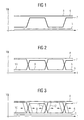
- FIG 4 is a circuit arrangement 1 with a first Voltage connection 2 a second voltage connection 3 and one Control input 4 shown.
- the circuit arrangement 1 there is a logical block which e.g. a MOS transistor or contains a CMOS inverter.
- voltage curves are described that are suitable for stress the circuit arrangement 1 and age prematurely to let the circuit arrangement 1 a constant Behavior assumes.
- FIG 2 is another embodiment of an inventive Voltage curve shown.
- the difference to Figure 1 is that in Figure 2, the second voltage 6 not kept constant at the value of the operating voltage 8 is, but between the reference potential 5 and the operating voltage 8 alternates.
- the two frequencies are identical, the corresponding ones However, voltages have a phase shift of about 180 degrees.
- the second voltage reaches you high voltage value when the control voltage is low Voltage value, and vice versa. By doing this the circuit arrangement 1 is accelerated in its aging process.
- FIG. 3 is another embodiment of an inventive Voltage curve shown.
- the phase position of the second voltage 6 in FIG. 3 and the control voltage 7 is not constant at 180 degrees, but can be varied within a range of ⁇ 30 degrees.
- the variation of the phase position becomes the stress on the circuit arrangement 1 further increased so that the accelerated Aging (burn-in) of the circuit arrangement 1 takes time can be reduced in an advantageous manner.
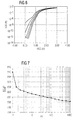
- FIG. 5 shows an input characteristic field of a P-channel transistor which was recorded directly after the P-channel transistor was manufactured.
- the five characteristic curves shown belong to different source-drain voltages, whereby the lowest characteristic curve can be assigned to the lowest source-drain voltage and the top characteristic curve to the highest source-drain voltage. It can be seen that the transistor shows good switch-off behavior with 10 -11 amperes even at high source-drain voltages.
- FIG. 6 shows the input characteristic field of the transistor known from FIG. 5 after the burn-in process according to the invention. It can be clearly seen that the switch-off behavior at high source-drain voltages is no longer very good, since source-drain currents of 10 -7 amperes flow, which is a factor 10000 greater than before the burn-in process.
- the principle of operation is that one is in the memory existing frequency the transistors of the circuit on and turns off.
- the transistors have gate and drain connections thereby via contacts with that generated on the memory chip and connected to the frequency clocked voltage.
Landscapes
- Dram (AREA)
- Tests Of Electronic Circuits (AREA)
- For Increasing The Reliability Of Semiconductor Memories (AREA)
- Testing Of Individual Semiconductor Devices (AREA)
Applications Claiming Priority (2)
| Application Number | Priority Date | Filing Date | Title |
|---|---|---|---|
| DE10014388 | 2000-03-23 | ||
| DE10014388A DE10014388A1 (de) | 2000-03-23 | 2000-03-23 | Verfahren zur Durchführung eines Burn-in-Prozesses eines Speichers |
Publications (2)
| Publication Number | Publication Date |
|---|---|
| EP1136833A1 true EP1136833A1 (fr) | 2001-09-26 |
| EP1136833B1 EP1136833B1 (fr) | 2005-01-26 |
Family
ID=7636020
Family Applications (1)
| Application Number | Title | Priority Date | Filing Date |
|---|---|---|---|
| EP01104285A Expired - Lifetime EP1136833B1 (fr) | 2000-03-23 | 2001-02-22 | Méthode d' exécution d' un procédé de vieillissement par contrainte électrique pour une mémoire à semi-conducteur |
Country Status (4)
| Country | Link |
|---|---|
| US (1) | US6445630B2 (fr) |
| EP (1) | EP1136833B1 (fr) |
| DE (2) | DE10014388A1 (fr) |
| TW (1) | TW525179B (fr) |
Families Citing this family (10)
| Publication number | Priority date | Publication date | Assignee | Title |
|---|---|---|---|---|
| US6891404B2 (en) * | 2002-06-11 | 2005-05-10 | Infineon Technologies | Auto-adjustment of self-refresh frequency |
| US6969618B2 (en) * | 2002-08-23 | 2005-11-29 | Micron Technology, Inc. | SOI device having increased reliability and reduced free floating body effects |
| EP3308744B2 (fr) | 2004-03-11 | 2023-08-02 | Percutaneous Cardiovascular Solutions Pty Limited | Prothèse de valvule cardiaque percutanée |
| US20060169281A1 (en) * | 2005-02-03 | 2006-08-03 | Aylsworth Alonzo C | Continuous flow selective delivery of therapeutic gas |
| WO2010057262A1 (fr) | 2008-11-21 | 2010-05-27 | Percutaneous Cardiovascular Solutions Pty Limited | Prothèse de valve cardiaque et procédé |
| JP6179158B2 (ja) * | 2013-03-27 | 2017-08-16 | 三菱電機株式会社 | トランジスタの製造方法、増幅器の製造方法 |
| RU2554660C1 (ru) * | 2013-12-06 | 2015-06-27 | Максимов Владимир Алексеевич | Способ электротермотренировки интегральных микросхем |
| JP6292104B2 (ja) * | 2014-11-17 | 2018-03-14 | 三菱電機株式会社 | 窒化物半導体装置の製造方法 |
| US11115022B2 (en) * | 2015-05-07 | 2021-09-07 | Northwestern University | System and method for integrated circuit usage tracking circuit with fast tracking time for hardware security and re-configurability |
| CN107202946B (zh) * | 2017-05-22 | 2019-07-02 | 西安电子科技大学 | Cmos反相器mos阈值电压的测量方法 |
Citations (5)
| Publication number | Priority date | Publication date | Assignee | Title |
|---|---|---|---|---|
| WO1982000917A1 (fr) * | 1980-09-08 | 1982-03-18 | Proebsting R | Circuit de vieillissement accelere de bande |
| US5557559A (en) * | 1992-07-06 | 1996-09-17 | Motay Electronics, Inc. | Universal burn-in driver system and method therefor |
| DE19603107A1 (de) * | 1995-12-26 | 1997-07-03 | Lg Semicon Co Ltd | Selbst-Voralterungsschaltung für Halbleiterspeicher |
| US5872797A (en) * | 1996-12-02 | 1999-02-16 | International Business Machines Corporation | Burn-in signal pattern generator |
| US6038181A (en) * | 1998-08-18 | 2000-03-14 | Internatioal Business Machines Corp. | Efficient semiconductor burn-in circuit and method of operation |
Family Cites Families (9)
| Publication number | Priority date | Publication date | Assignee | Title |
|---|---|---|---|---|
| US4751679A (en) * | 1986-12-22 | 1988-06-14 | Motorola, Inc. | Gate stress test of a MOS memory |
| KR950014099B1 (ko) * | 1992-06-12 | 1995-11-21 | 가부시기가이샤 도시바 | 반도체 기억장치 |
| JP2885597B2 (ja) | 1993-03-10 | 1999-04-26 | 株式会社東芝 | 半導体メモリ |
| KR0122107B1 (ko) | 1994-06-04 | 1997-12-05 | 김광호 | 저전력 셀프리프레쉬 및 번-인 기능을 가지는 반도체메모리장치 |
| KR970001564U (ko) | 1995-06-21 | 1997-01-21 | 자동차용 후부차체의 보강구조 | |
| US5898186A (en) | 1996-09-13 | 1999-04-27 | Micron Technology, Inc. | Reduced terminal testing system |
| KR100228530B1 (ko) | 1996-12-23 | 1999-11-01 | 윤종용 | 반도체 메모리 장치의 웨이퍼 번인 테스트회로 |
| JP4046382B2 (ja) | 1997-03-27 | 2008-02-13 | 株式会社ルネサステクノロジ | 半導体集積回路装置 |
| KR100268434B1 (ko) | 1997-12-29 | 2000-10-16 | 윤종용 | 반도체 메모리 장치 및 그것의 번-인 테스트방법 |
-
2000
- 2000-03-23 DE DE10014388A patent/DE10014388A1/de not_active Withdrawn
-
2001
- 2001-02-22 EP EP01104285A patent/EP1136833B1/fr not_active Expired - Lifetime
- 2001-02-22 DE DE50105160T patent/DE50105160D1/de not_active Expired - Lifetime
- 2001-03-22 TW TW090106783A patent/TW525179B/zh not_active IP Right Cessation
- 2001-03-23 US US09/816,924 patent/US6445630B2/en not_active Expired - Lifetime
Patent Citations (5)
| Publication number | Priority date | Publication date | Assignee | Title |
|---|---|---|---|---|
| WO1982000917A1 (fr) * | 1980-09-08 | 1982-03-18 | Proebsting R | Circuit de vieillissement accelere de bande |
| US5557559A (en) * | 1992-07-06 | 1996-09-17 | Motay Electronics, Inc. | Universal burn-in driver system and method therefor |
| DE19603107A1 (de) * | 1995-12-26 | 1997-07-03 | Lg Semicon Co Ltd | Selbst-Voralterungsschaltung für Halbleiterspeicher |
| US5872797A (en) * | 1996-12-02 | 1999-02-16 | International Business Machines Corporation | Burn-in signal pattern generator |
| US6038181A (en) * | 1998-08-18 | 2000-03-14 | Internatioal Business Machines Corp. | Efficient semiconductor burn-in circuit and method of operation |
Also Published As
| Publication number | Publication date |
|---|---|
| DE10014388A1 (de) | 2001-10-04 |
| US6445630B2 (en) | 2002-09-03 |
| DE50105160D1 (de) | 2005-03-03 |
| EP1136833B1 (fr) | 2005-01-26 |
| TW525179B (en) | 2003-03-21 |
| US20010033518A1 (en) | 2001-10-25 |
Similar Documents
| Publication | Publication Date | Title |
|---|---|---|
| DE3032657C2 (fr) | ||
| DE3041176A1 (de) | Halbleiterspeichervorrichtung | |
| DE19603447C2 (de) | Integrierte Halbleiterschaltungsvorrichtung | |
| EP1136833B1 (fr) | Méthode d' exécution d' un procédé de vieillissement par contrainte électrique pour une mémoire à semi-conducteur | |
| WO2007118679A1 (fr) | Agencement de circuit comprenant une cellule à mémoire non volatile, et procédé correspondant | |
| DE102005061375B4 (de) | NOR-Flashspeicherbauelement mit Mehrpegel-Speicherzelle und Bitwert-Detektionsverfahren | |
| DE19622646B4 (de) | Integrierte Halbleiterschaltungsvorrichtung | |
| DE69329543T2 (de) | Herstellung eines Feldeffekttransistors mit integrierter Schottky-Klammerungsdiode | |
| DE3722421C2 (fr) | ||
| DE19934297C1 (de) | Integrierte Halbleiterschaltung mit erhöhter Betriebsspannung für programmierbare Elemente (z.B. zur Konfigurierung) | |
| EP1153394B1 (fr) | Procede pour faire fonctionner un ensemble de cellules memoires comportant des cellules memoires dynamiques a auto-amplification | |
| DE2749711A1 (de) | Verfahren und anordnung zur beeinflussung und erfassung von ladungstraegerinjektionsvorgaengen in feldeffektbauelementen | |
| EP0045403B1 (fr) | Méthode de production de cellules de memoire MOS pour réduire l'influence d'irradiation | |
| DE4336883A1 (de) | Verbesserte Ausgangstreiberschaltung zum Unterdrücken von Rauscherzeugung und verbesserte integrierte Halbleiterschaltungseinrichtung zum Einbrenntest | |
| DE2550276A1 (de) | Kapazitiver datenspeicher | |
| DE2433077A1 (de) | Dynamische speichereinrichtung | |
| DE2450882A1 (de) | Komplementaere mos-logische schaltung | |
| DE3032306C2 (fr) | ||
| DE102020101267A1 (de) | Ausgeglichene negative Bitleitungsspannung für eine Schaltung mit Schreibunterstützung | |
| DE102005009050B4 (de) | Differentielle Ausleseschaltung für Fuse-Speicherzellen | |
| DE2360887A1 (de) | Komplementaer-speicherelement | |
| DE10344872A1 (de) | Integrierte Schaltung mit Schutz vor elektrostatischer Entladung | |
| DE10211932B4 (de) | Schaltungsanordnung zum Auslesen, Bewerten und Wiedereinlesen eines Ladungszustandes in eine Speicherzelle | |
| DE69422220T2 (de) | Ausgangsschaltung mit drei Speisespannungen | |
| DE2261522A1 (de) | Halbleiterspeichereinheit |
Legal Events
| Date | Code | Title | Description |
|---|---|---|---|
| PUAI | Public reference made under article 153(3) epc to a published international application that has entered the european phase |
Free format text: ORIGINAL CODE: 0009012 |
|
| AK | Designated contracting states |
Kind code of ref document: A1 Designated state(s): AT BE CH CY DE DK ES FI FR GB GR IE IT LI LU MC NL PT SE TR Kind code of ref document: A1 Designated state(s): DE FR GB |
|
| AX | Request for extension of the european patent |
Free format text: AL;LT;LV;MK;RO;SI |
|
| 17P | Request for examination filed |
Effective date: 20020326 |
|
| AKX | Designation fees paid |
Free format text: DE FR GB |
|
| 17Q | First examination report despatched |
Effective date: 20030925 |
|
| GRAP | Despatch of communication of intention to grant a patent |
Free format text: ORIGINAL CODE: EPIDOSNIGR1 |
|
| GRAS | Grant fee paid |
Free format text: ORIGINAL CODE: EPIDOSNIGR3 |
|
| GRAA | (expected) grant |
Free format text: ORIGINAL CODE: 0009210 |
|
| AK | Designated contracting states |
Kind code of ref document: B1 Designated state(s): DE FR GB |
|
| REG | Reference to a national code |
Ref country code: GB Ref legal event code: FG4D Free format text: NOT ENGLISH |
|
| REF | Corresponds to: |
Ref document number: 50105160 Country of ref document: DE Date of ref document: 20050303 Kind code of ref document: P |
|
| GBT | Gb: translation of ep patent filed (gb section 77(6)(a)/1977) |
Effective date: 20050413 |
|
| PLBE | No opposition filed within time limit |
Free format text: ORIGINAL CODE: 0009261 |
|
| STAA | Information on the status of an ep patent application or granted ep patent |
Free format text: STATUS: NO OPPOSITION FILED WITHIN TIME LIMIT |
|
| ET | Fr: translation filed | ||
| 26N | No opposition filed |
Effective date: 20051027 |
|
| PGFP | Annual fee paid to national office [announced via postgrant information from national office to epo] |
Ref country code: GB Payment date: 20070216 Year of fee payment: 7 |
|
| PGFP | Annual fee paid to national office [announced via postgrant information from national office to epo] |
Ref country code: FR Payment date: 20080214 Year of fee payment: 8 |
|
| GBPC | Gb: european patent ceased through non-payment of renewal fee |
Effective date: 20080222 |
|
| PG25 | Lapsed in a contracting state [announced via postgrant information from national office to epo] |
Ref country code: GB Free format text: LAPSE BECAUSE OF NON-PAYMENT OF DUE FEES Effective date: 20080222 |
|
| REG | Reference to a national code |
Ref country code: FR Ref legal event code: ST Effective date: 20091030 |
|
| PG25 | Lapsed in a contracting state [announced via postgrant information from national office to epo] |
Ref country code: FR Free format text: LAPSE BECAUSE OF NON-PAYMENT OF DUE FEES Effective date: 20090302 |
|
| REG | Reference to a national code |
Ref country code: DE Ref legal event code: R081 Ref document number: 50105160 Country of ref document: DE Owner name: INFINEON TECHNOLOGIES AG, DE Free format text: FORMER OWNER: QIMONDA AG, 81739 MUENCHEN, DE Ref country code: DE Ref legal event code: R081 Ref document number: 50105160 Country of ref document: DE Owner name: POLARIS INNOVATIONS LTD., IE Free format text: FORMER OWNER: QIMONDA AG, 81739 MUENCHEN, DE |
|
| PGFP | Annual fee paid to national office [announced via postgrant information from national office to epo] |
Ref country code: DE Payment date: 20150414 Year of fee payment: 15 |
|
| REG | Reference to a national code |
Ref country code: DE Ref legal event code: R081 Ref document number: 50105160 Country of ref document: DE Owner name: POLARIS INNOVATIONS LTD., IE Free format text: FORMER OWNER: INFINEON TECHNOLOGIES AG, 85579 NEUBIBERG, DE |
|
| REG | Reference to a national code |
Ref country code: DE Ref legal event code: R119 Ref document number: 50105160 Country of ref document: DE |
|
| PG25 | Lapsed in a contracting state [announced via postgrant information from national office to epo] |
Ref country code: DE Free format text: LAPSE BECAUSE OF NON-PAYMENT OF DUE FEES Effective date: 20160901 |